

VIPer50/SP
TYPE V
DSS
I
R
n
DS(on)
VI Per 5 0/ SP 620V 1.5 A 5 Ω
VI Per 5 0A /ASP 700V 1.5 A 5.7 Ω
FEATURE
■ ADJUSTABLESWITCHING FREQUENCY UP
TO200KHZ
■ CURRENT MODE CONTROL
■ SOFTSTART ANDSHUT DOWN CONTROL
■ AUTOMATIC BURST MODE OPERATION IN
STAND-BY CONDITION ABLE TO MEET
”BLUE ANGEL” NORM(<1W TOTAL POWER
CONSUMPTION)
■ INTERNALLY TRIMMED ZENER
REFERENCE
■ UNDERVOLTAGE LOCK-OUT WITH
HYSTERESIS
■ INTEGRATED START-UPSUPPLY
■ AVALANCHERUGGED
■ OVERTEMPERATURE PROTECTION
■ LOW STAND-BYCURRENT
■ ADJUSTABLECURRENTLIMITATION
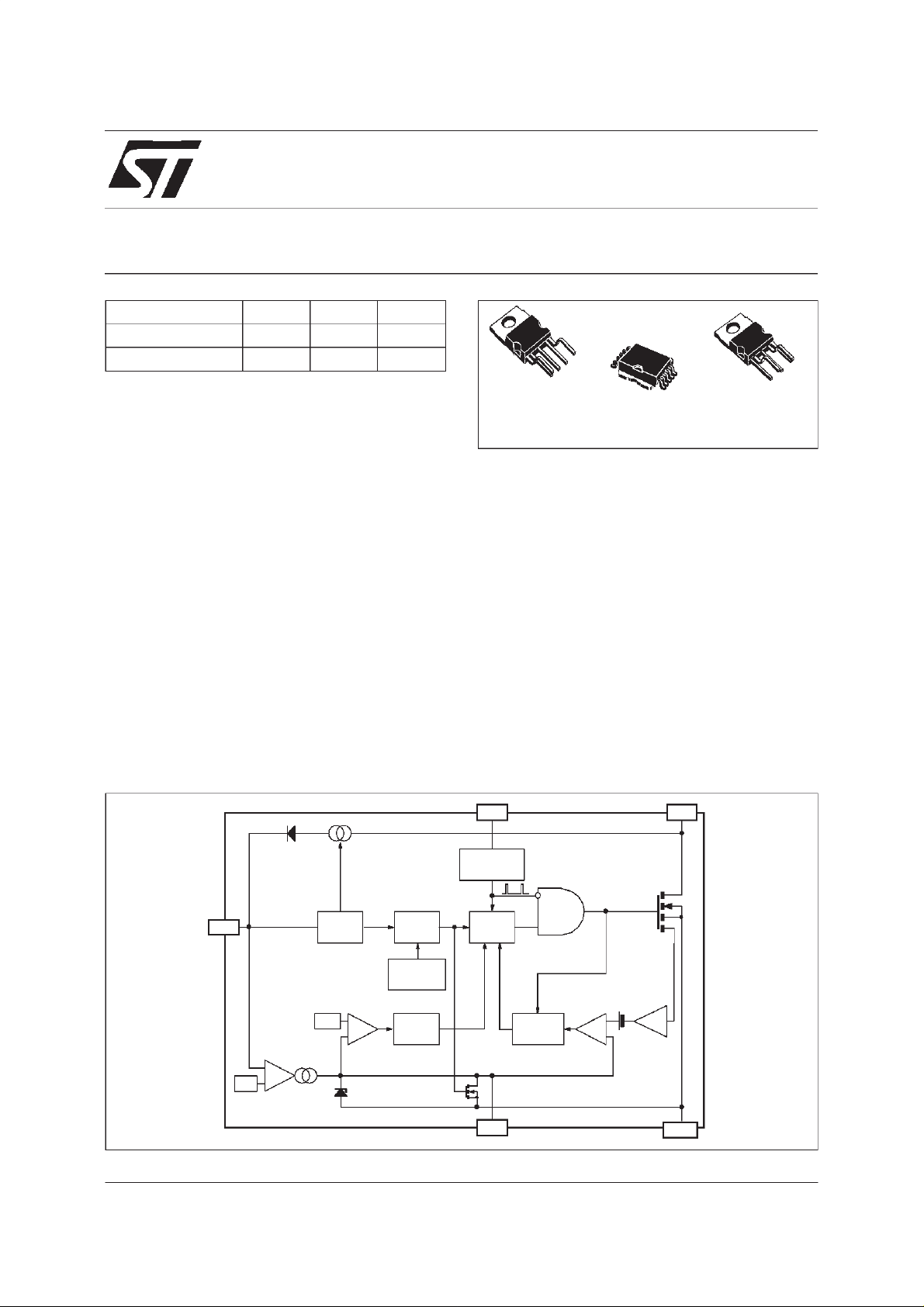
BLOCK DIAGRAM
VIPer50A/ASP
SMPS PRIMARY I.C.
10
PENTAWATTHV PENTAWATT HV
PowerSO-10
DESCRIPTION
VIPer50/50A make using VIPower M0
Technology combines on the same silicon chip a
state-of-the-art PWM circuit together with an
optimized high voltage avalancherugged Vertical
Power MOSFET (620Vor 700V / 1.5A).
Typical applications cover off line power supplies
with a secondary power capabilityof 25W in wide
range condition and 50W in single range or with
doubler configuration. It is compatible from both
primary or secondary regulation loop despite
using around 50% less components when
compared with a discrete solution. Burst mode
operation is an additional feature of this device,
offering the possibility to operate in stand-by
mode withoutextra components.
1
(022Y)
May 1999
_
2 V/A
CURRENT
AMPLIFIER
DRAIN
SOURCE
1
9
2
0
0
C
F
OSC
ON/OFF
SECURITY
LATCH
FF
R/SSQ
OVERTEMP.
DETECTOR
1.7µs
DELAY
ERROR
AMPLIFIER_
LOGIC
0.5 V
UVLO
+
_
4.5 V
VDD
13 V
+
OSCILLATOR
PWM
LATCH
S
R1
FF
R2 R3
COMP
Q
250 ns
BLANKING
0.5V
+
+
_
1/20
VIPer50/SP - VIPer50A/ASP
ABSOLUTEMAXIMUMRATING
Symb o l Para met er Val u e Uni t
V
I
V
V
OSC
V
COMP
I
COMP
V
I
D(AR)
P
T
T
THERMALDATA
R
thj-case
R
thj-a mb.
(*) When mounted using the minimum recommended pad size on FR-4 board.
Continuous Drain- Sour ce Volta ge (Tj = 25 t o 125oC)
DS
for VIPer50/S P
for VIPer50A/ ASP
Maximum Current Inte rnally Li mited A
D
Supply Volt age 0 to 15 V
DD
Volt age Range Input 0 t o V
-0.3 to 620
-0.3 to 700
DD
Volt age Range Input 0 t o 5 V
Maximum Continuous Cur rent ±2mA
Elect r o st at ic discharge (R = 1.5 KΩ C = 100pF) 4000 V
esd
Avalanche Drain-Source Curre nt , Repetitive or N ot -Repet it ive
(T C = 100
for VIPer50/S P
for VIPer50A/ ASP
Power Dissipation at Tc = 25oC60W
tot
Junction Operatin g Temperature Int ernally Limited
j
St orage T emperature -65 to 150
stg
o
C, Pulse Width Limited by TJmax, δ <1%)
1.5
1
PENTAWATT-HV PowerSO-10(*)
Ther mal Res istan ce Junc ti on-c ase Max 1.9 1.9
Ther mal Res istan ce Ambient-case Max 60 50
o
o
o
C/W
o
C/W
V
V
V
A
A
C
C
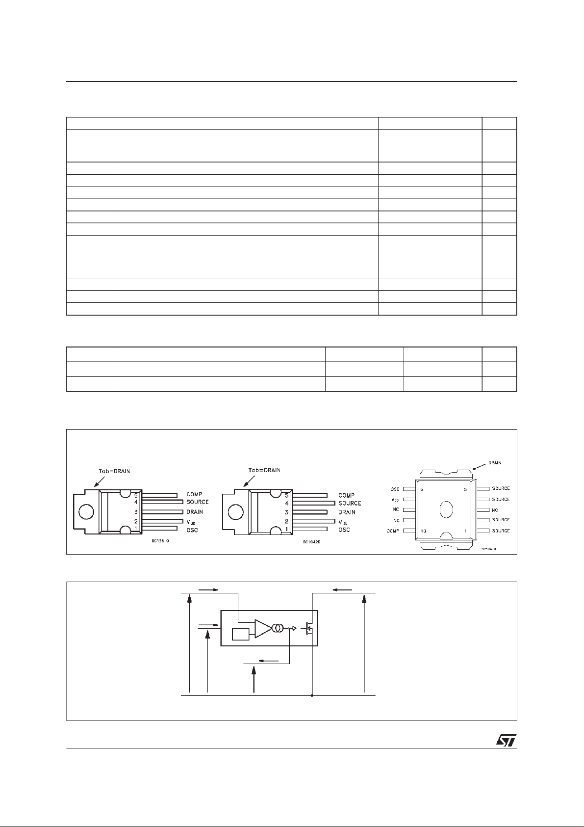
CONNECTION DIAGRAMS (Top View)
PENTAWATTHV PENTAWATTHV (022Y) PowerSO-10
CURRENT AND VOLTAGE CONVENTIONS
IDD ID
OSC
I
OSC
DD
V
13V
OSC
V
+
ICOMP
VCOMP
DRAINVDD
COMP SOURCE
VDS
2/20
FC00020

ORDERING NUMBERS
PENTAWATT HV PENT AWATT HV (022Y) PowerSO - 10
VIPer50
VIPer50A
VIPer50 ( 022Y)
VI Per50A (022Y)
VIPer50/SP - VIPer50A/ASP
VIP er 50SP
VIPer50ASP
PINSFUNCTIONAL DESCRIPTION
DRAINPIN:
Integrated power MOSFET drain pin. It provides
internal bias current during start-up via an
integrated high voltage current source which is
switched off during normal operation. The device
is able to handle an unclamped current during its
normal operation, assuring self protection against
voltage surges, PCB stray inductance, and
allowing a snubberless operation for low output
power.
SOURCEPIN:
Power MOSFET source pin. Primary side circuit
commonground connection.
VDD PIN :
This pin provides two functions:
- It corresponds to the low voltage supply of the
controlpart of the circuit. If V
the start-up current source is activated and the
output power MOSFET is switched off untilthe
V
voltage reaches 11V. During this phase,
DD
the internal current consumption is reduced,
the V
pin is sourcing a currentof about 2mA
DD
and the COMP pin is shorted to ground. After
that, the current source is shut down, and the
devicetries to start upby switchingagain.
goes below 8V,
DD
- This pin is also connected to the error
amplifier, in order to allow primary as well as
secondary regulation configurations.In case of
primary regulation, an internal 13V trimmed
reference voltage is used to maintain V
13V. For secondary regulation, a voltage
between 8.5V and 12.5V will be puton V
by transformer design, in order to stuck the
output of the transconductanceamplifier to the
high state. The COMP pin behaves as a
DD
DD
at
pin
constant current source, and can easily be
connected to the output of an optocoupler.
Note that any overvoltage due to regulation
loop failure is still detected by the error
amplifier through the V
voltage, which
DD
cannot overpass 13V. The output voltage will
be somewhathigher than the nominalone, but
still undercontrol.
COMP PIN :
This pin providestwo functions :
- It is the output of the error transconductance
amplifier, and allows for the connection of a
compensation network to provide the desired
transfer function of the regulation loop. Its
bandwidth can be easily adjusted to the
needed value with usual componentsvalue. As
stated above, secondary regulation
configurations are also implemented through
the COMPpin.
- When the COMP voltage is going below 0.5V,
the shut-downof thecircuit occurs, with a zero
duty cycle for thepower MOSFET. This feature
can be used to switchoff the converter, and is
automatically activated by the regulation loop
(whatever is the configuration) to provide a
burst mode operation in case of negligible
output power or open load condition.
OSC PIN :
An R
to define the switching frequency. Note that
despite the connection of R
significant frequency change occurs for V
varying from 8V to 15V. It provides also a
synchronisationcapability, when connected to an
external frequency source.
network must be connected on that pin
T-CT
to VDD,no
T
DD
3/20
VIPer50/SP - VIPer50A/ASP
AVALANCHE CHARACTERISTICS
Symb o l Para met er Max Valu e Uni t
I
D(ar)
E
ELECTRICAL CHARACTERISTICS (TJ=25oC, VDD=13 V,unless otherwise specified)
POWERSECTION
Symb o l Paramet er Test Con d it i ons Min. Typ . Max. Unit
BV
I
DSS
R
DS(on)
C
OSS
(1) OnInductive Load, Clamped.
Avalanche Current, Repetitive or Not-Repet it ive
(pulse widt h limited by T
for VIPer50/S P
for VIPer50A/ ASP (see f ig. 12)
Single Pulse Avalanche Ener g y
(ar)
(starti ng T
Drain-Source Voltage ID=1mA V
DSS
=25oC, ID=I
j
Of f - State Dra in Curr ent V
St at ic Drain Source on
Resistance
max, δ <1%)
j
) (see fig. 12)
D(ar)
COMP
for VIPer50/SP
for VIPer50A/ASP (see fig. 5)
=0V TJ=125oC
COMP
V
= 620 V for VI P er5 0/ SP
DS
= 700 V for VI P er5 0A/AS P
V
DS
ID=1A
for VIPer50/SP
for VIPer50A/ASP
=1A TJ= 100oC
I
D
1.5
1.0
30 mJ
=0V
620
700
4.0
4.6
for VIPer50/SP
for VIPer50A/ASP
t
Fall Time ID = 0.2 A Vin= 300 V (1)
f
100 ns
(see f ig. 3)
Rise Time ID=1A Vin= 300 V (1)
t
r
50 ns
(see f ig. 3)
Out put Capacitance VDS= 25 V 120 pF
1
1
5.0
5.7
9.0
10.3
A
A
V
V
mA
mA
Ω
Ω
Ω
Ω
SUPPLY SECTION
Symb o l Paramet er Test Con d it i ons Min. Typ . Max. Unit
4/20
I
DDch
I
DD0
I
DD1
I
DD2
V
DDo f f
V
DDo n
V
DDhyst
St art - u p Charging
Current
Oper at i ng Supply Current VDD=12V, FSW=0KHz
VDD=5V VDS=70V
(see fig. 2 and fig . 15)
-2 mA
12 16 mA
(see f ig. 2)
Oper at i ng Supply Current VDD=12V, FSW= 100 KHz 14 mA
Oper at i ng Supply Current VDD=12V, FSW= 200 KHz 16 mA
Undervoltage S hutdown (see fig. 2) 8 V
Undervoltage Reset (see fig. 2) 11 12 V
Hysteresis Start-up (see f ig. 2) 2.4 3 V

VIPer50/SP - VIPer50A/ASP
ELECTRICAL CHARACTERISTICS (continued)
OSCILLATORSECTION
Symb o l Paramet er Test Con d it i ons Min. Typ . Max. Unit
F
Os cillator Frequen cy
SW
Total Variation
RT= 8.2 K
= 9 to15 V
V
DD
with R
± 1% CT ± 5%
T
Ω
CT=2.4 nF
(see fig.6 and fig.9)
V
V
OSCih
OSCil
Os cillator Peak Voltage 7.1 V
Os cillator Valley Voltage 3 . 7 V
ERRORAMPLIFIERSECTION
Symbol Parameter Test Condition s Min. Typ. Max. Unit
V
DDreg
∆V
DDreg
G
A
VOL
G
V
COMPLO
V
COMPHI
I
COMPLO
I
COMPHI
VDD Regulat ion Point I
= 0 mA (s e e fig.1) 12.6 13 13.4 V
COMP
Total Variation TJ= 0 to 100oC2%
Unity Gain Bandwidt h F rom Input = VDDto Output = V
BW
COMP
COM P pin i s open (see fig. 10 )
Open Loop Voltage
COM P pin i s open (see fig. 10 ) 45 5 2 dB
Gain
DC Transconductance V
m
Out put Low Level I
Out put High L ev el I
Out put Low Current
= 2.5 V (s ee fig. 1 ) 1.1 1.5 1.9 mA/V
COMP
=-400µAVDD=14V 0.2 V
COMP
= 400 µAVDD=12V 4.5 V
COMP
V
=2.5V VDD= 14 V -600 µA
COMP
Capability
Out put High C ur rent
V
=2.5V VDD= 12 V 600 µA
COMP
Capability
90 100 110 KHz
150 KHz
PWM COMPARATORSECTION
Symbol Parameter Test Condition s Min. Typ. Max. Unit
H
V
COMPoffVCOMP
I
Dpeak
t
∆V
ID
/∆I
COMP
Dpeak
off s et I
V
= 1 to 3 V 1.4 2 2.6 V/A
COMP
=10mA 0.5 V
Dpeak
Peak Current Limitation VDD=12V COMPpinopen 1.5 2 2.7 A
Current Sense Delay
d
ID= 0. 5 A 250 ns
to turn-off
t
t
on(min)
Blanking Time 250 360 ns
b
Minimum on T ime 350 ns
SHUTDOWNAND OVERTEMPERATURESECTION
Symbol Parameter Test Condition s Min. Typ. Max. Unit
V
COMPth
t
DISsu
T
T
hyst
Restart threshold (see fig. 4) 0.5 V
Disable Set Up Time (see fig. 4 ) 1.7 5 µ s
Ther mal Shut down
tsd
(see fig. 8 ) 140 170
Tem perature
Ther mal Shut down
(see fig. 8 ) 40
Hyst eresis
o
o
C
C
5/20
VIPer50/SP - VIPer50A/ASP
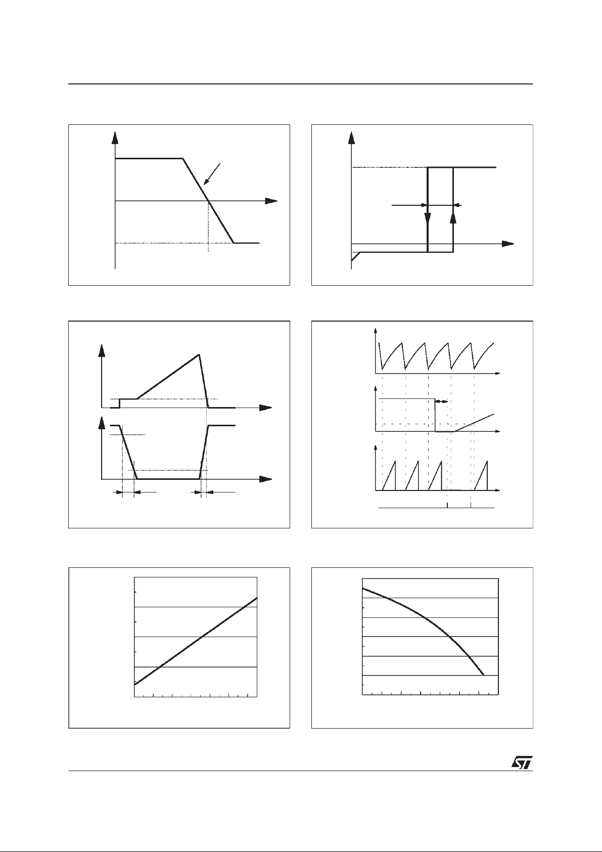
Figure1:VDDRegulationPoint
COMP
I
ICOMPHI
0
ICOMPLO
VDDreg
Figure3: TransitionTime
ID
10%Ipeak
Slope =
Gm in mA/V
FC00150
Figure2: UndervoltageLockout
IDD
IDD0
DD
V
VDDhyst
V
DDoff
IDDch
Figure4: ShutDown Action
VOSC
VCOMP
t
tDISsu
VDS=70V
Fsw = 0
V
DDon
FC00170
VDD
t
VDS
VCOMPth
90%VD
ID
10%V
D
t
tf tr
FC00160
ENABLE
DISABLE
Figure5: Breakdown Voltage vs Temperature Figure6: Typical FrequencyVariation
1.15
BV
DSS
(Normalized)
1.1
1.05
0.95
1
0 20 40 60 80 100 120
Temperature (°C)
FC00180
1
(%)
0
-1
-2
-3
-4
-5
0 20 40 60 80 100 120 140
Temperature (°C)
t
t
ENABLE
FC00060
FC00190
6/20
 Loading...