

SGS Thomson Microelectronics VIPER12AS, VIPER12ADIP Datasheet
VIPer12ADI P
®
LOW POWER OFF LINE SMPS PRIMARY SWITCHER
TYPICAL POWER CA PABILITY
Main s t y pe SO-8 DIP8
European
(195 - 265 Vac)
US / Wide range
(85 - 265 Vac)
n
FIXED 60 KHZ SWITCHING FREQUENCY
n
9V TO 38V WIDE RANGE V
n
CURRENT MODE CONTROL
n
AUXILIARY UNDERVOLTAGE LOCKOUT
WITH HYSTERESIS
n
HIGH VOLTAGE START UP CURRENT
SOURCE
n
O VERTEMPERATURE, OVE RCURRENT AND
OVERVOLTAGE PROTECTION WITH
AUTORESTAR T
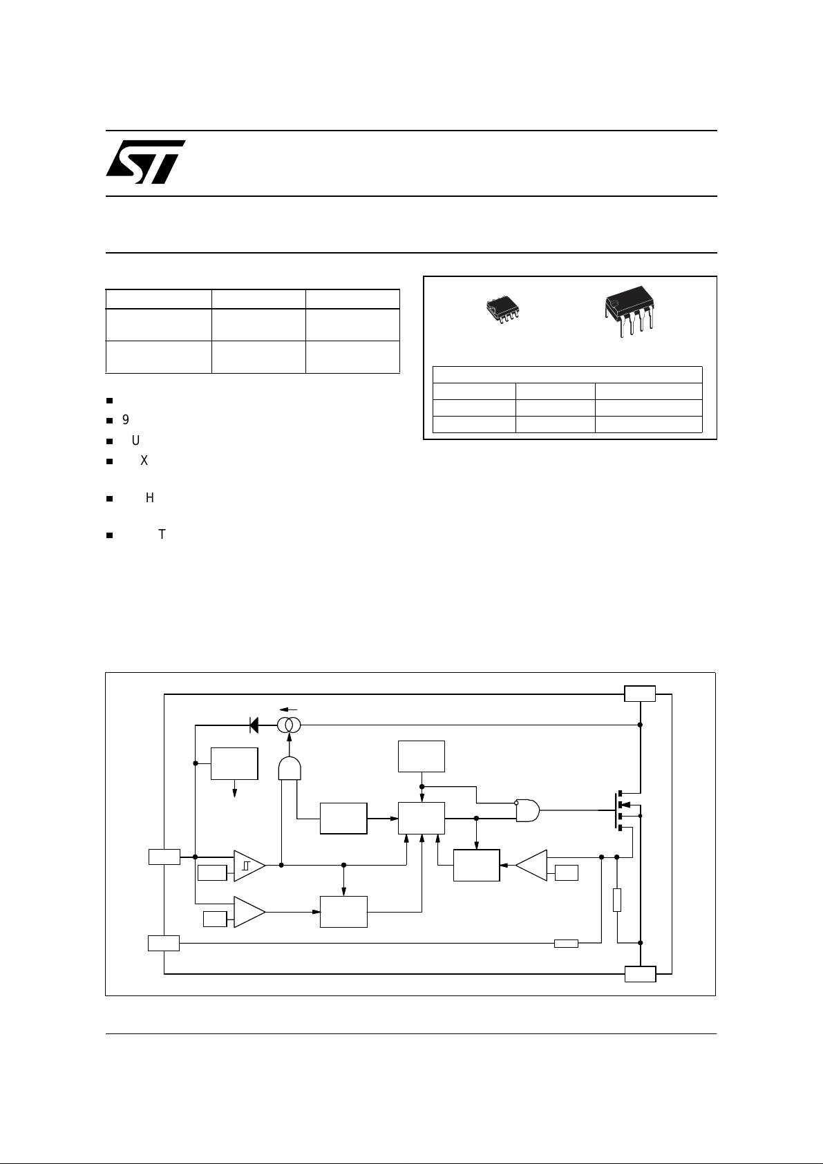
DESCRIPTION
The VIPer12A combines a dedicated current mode
PWM controller with a high voltage Power
8 W 13 W
5 W 8 W
VOLTAGE
DD
VIPer12AS
SO-8 DIP-8
ORDER CODES
PACKAGE TUBE T&R
SO-8 VIPer12AS VIPer12AS13TR
DIP-8 VIPer12ADIP
MOSFET on the same silicon chip. Typical
applications cover off line power supplies for
battery charg er adapter s, stan dby pow er suppl ies
for TV or monitors, auxiliary supplies for motor
control, etc. The i nternal control circuit offers the
following benefits:
– Large input voltage range on the VDD pin
accommodates changes in auxiliary supply
voltage. This fe ature is well adapted to battery
charger adapter configurations.
– Automatic burst mode in low load condition.
– Overvoltage protection in hiccup mode.
BLO C K DIAGRA M
DRAIN
ON/OFF
REGULATOR
INTERNAL
VDD
FB
8/14.5V
42V
SUPPLY
_
+
+
_
OVERTEMP.
DETECTOR
R
FF
S
OVERVOLTAGE
Q
Septe m ber 2002 1/15
LATCH
60kHz
OSCILLATOR
S
FF
R1
R4QR3
R2
PWM
LATCH
BLANKING
+
_
0.23 V
230
Ω
1 k
Ω
SOURCE
VIPer12ADIP / VIPer12AS
PIN FUNCTION
Name Function
Power supply of the control circuits. Also provides a charging current during start up thanks to a high
voltage current sour ce connected to the drai n. For this p urpose, an hysteresis comparator mo nitors the
voltage and provides two thres holds:
V
DD
V
SOURCE Power MOSFET source and circuit ground reference.
DRAIN
FB
CURRENT AND VOLTAGE CONVENTIONS
- V
DD
: Voltage value (typically 14.5V) at whi ch the device starts switching and tur ns off the start up
DDon
curre nt source.
- V
: Voltage value (typically 8V) at which the device stops switching and turns on the start up current
DDoff
source.
Power MOSFET drain. Al so used by the internal high voltage cu rrent source during start up phase for
charging the extern al V
capacitor.
DD
Feedbac k input. The useful voltage range extends from 0V to 1V, and defines the pea k drain MOSFET
current. The current limitation, which corresponds to the maximum drain current, is obtained for a FB pin
shorted to the SOURCE pin.
I
DD
I
D
V
DD
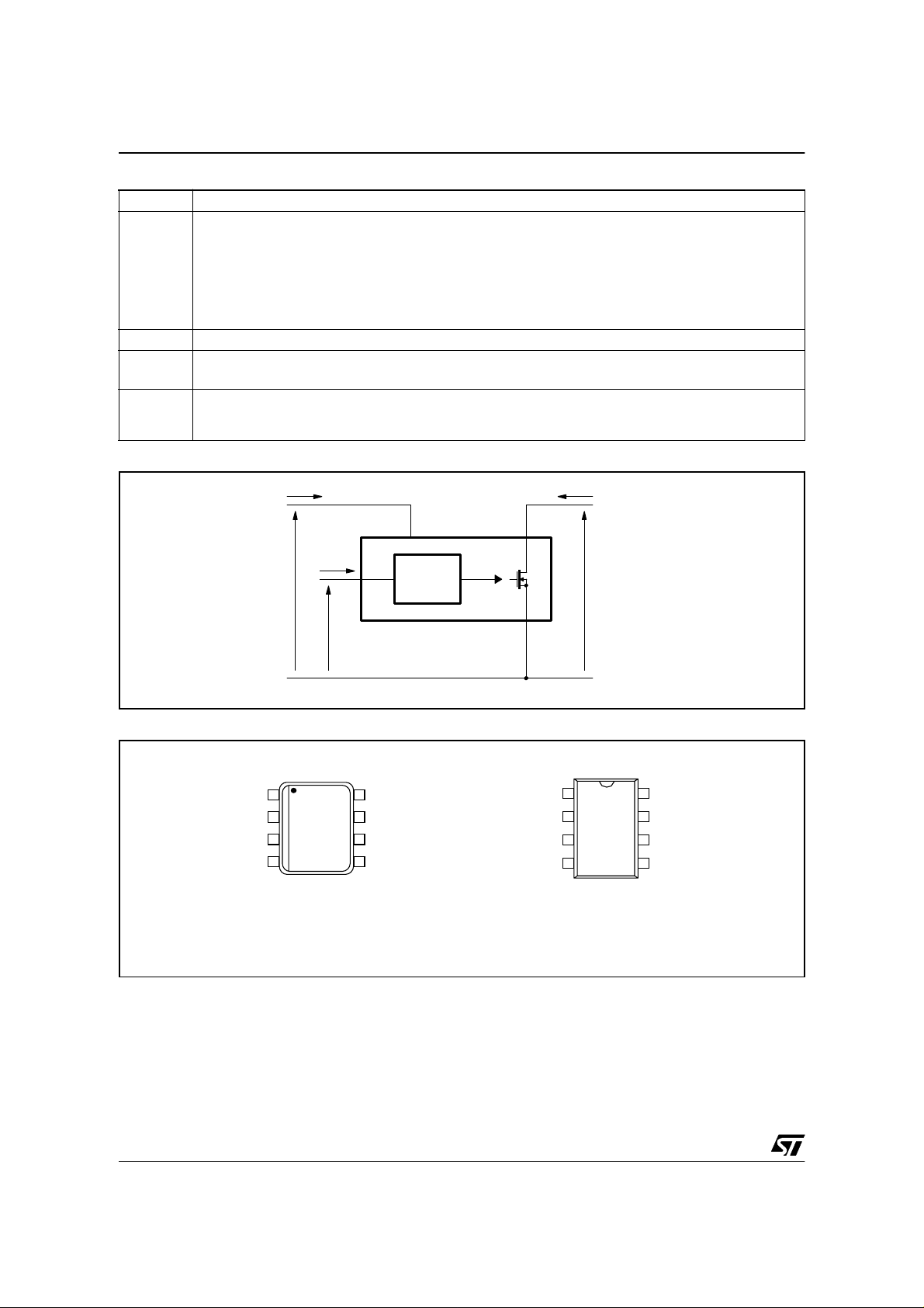
CONNECTION DIAGRAM
FB
VDD
1
2
3
4
SOURCE
SOURCE SOURCE
I
FB
V
FB
VDD DRAIN
FB
CONTROL
VIPer12A
8
DRAIN
7
DRAIN
6
DRAIN
5
DRAIN
SOURCE
SOURCE
FB
VDD
V
D
1
2
3
4
SO-8 DIP8
8
7
6
5
DRAIN
DRAIN
DRAIN
DRAIN
2/15

VIPer12ADIP / VIPer12AS
ABSOLUTE MAXIMUM RATI NGS
Symbol Parameter Value Unit
V
DS(sw)
V
DS(st)
I
V
I
FB
V
ESD
T
T
T
Note: 1. This parameter applies when the start up current source is off. This is the case when the VDD voltage has reached V
THERMAL DATA
Symbol Parameter Max Value Unit
Rthj-case
Rthj-amb
Note: 1. When mounted on a standard single-sided FR4 board with 200 mm² of Cu (at least 35 µm thick) connected to all DRAIN pins.
Switchin g Drain Source Voltage (Tj=25 ... 125 ° C) (See note 1)
Start Up Drain Source Voltage (Tj=25 ... 12 5°C) (See note 2)
Continuous Drain Current Internally limited A
D
Supply V o ltage 0 ... 50 V
DD
-0.3 ... 730 V
-0.3 ... 400 V
Feedbac k Current 3 mA
Electrostatic Discharge:
Machine Model (R=0Ω; C=200pF)
Charged Device Model
Junction Operating Temperature Internally limited °C
j
Case Oper ating Temperature -40 to 150 °C
c
Storage Temperature -55 to 150 °C
stg
remains ab ov e V
2. This parameter applies when the s tart up current source is on. This is the case when the V
or has fallen below V
DDoff
.
DDoff
.
DD
200
1.5
voltage has not yet reached V
Thermal Resistance Junction-P ins for:
SO-8
DIP8
25
15
Thermal Resistance Junction-A m bient for:
SO-8 (See note 1)
DIP8 (See note 1)
55
45
kV
DDon
°C/W
°C/W
V
and
DDon
ELECTRICAL CHARACTERISTICS (Tj=25°C, VDD=18V, unless otherwise specified)
POWER SECTION
Symbol Parameter Test Conditions Min. Typ. Max. Unit
BV
I
DSS
R
DSon
C
Note: 1. On clamped inductiv e load
Drain-Source Voltage
DSS
Off State Drain Current
Static Drain-Source
On State Resistance
t
Fall Time
f
t
Rise Time
r
Drain Capaci tance
oss
I
=1mA; VFB=2V
D
V
=500V; VFB=2V; Tj=125°C
DS
=0.2A
I
D
I
=0.2A; Tj=100°C
D
=0.1A; VIN=300V (See fig.1)
I
D
(See note 1)
=0.2A; VIN=300V (See fig.1)
I
D
(See note 1)
V
=25V
DS
730 V
0.1 mA
27 30
54
100 ns
50 ns
40 pF
Ω
3/15
VIPer12ADIP / VIPer12AS
ELECTRICAL CHARACTERISTICS (Tj=25°C, VDD=18V, unless otherwise specified)
SUPPLY SECTION
Symbol Parameter Test Conditions Min. Typ. Max. Unit
I
DDch
I
DDoff
I
DD0
I
DD1
D
RST
V
DDoff
V
DDon
V
DDhyst
V
DDovp
Note: 1. These test condit ions obtained with a resist iv e load are lead ing to the maxim um c onduction time of the device.
S ta r t Up Ch arging
Current
S ta r t Up Ch arging
Current
in Thermal Shutdown
Oper ating Supply Current
Not Switching
Oper ating Supply Current
Switching
DS=100V; V
V
=5V; VDS=100V
V
DD
> TSD - T
T
j
=2mA
I
FB
I
=0.5mA; ID=50mA (Note 1)
FB
DD
HYST
=5V ...V
(See fig. 2)
DDon
-1 mA
0mA
35mA
4.5 mA
Restart Duty Cycle (See fig. 3) 16 %
V
Undervoltage
DD
Shut do w n Th reshold
VDD Start Up Threshold
VDD Threshold
Hysteresis
VDD Overvo ltage
Threshold
(See fig. 2 & 3) 7 8 9 V
(See fig. 2 & 3) 13 14.5 16 V
(See fig. 2) 5.8 6.5 7.2 V
38 42 46 V
OSCILLATOR SECTION
Symbol Parameter Test Conditions Min. Typ. Max. Unit
F
OSC
Oscillator Frequency
Total Variation
V
DD=VDDoff
... 35V; Tj=0 ... 100°C
54 60 66 kHz
PWM COMPARATOR SECTION
Symbol Parameter Test Conditions Min. Typ. Max. Unit
G
I
Dlim
I
FBsd
R
t
t
t
ONmin
IFB to ID Current Gain
ID
V
Peak Current Limitation
=0V (See fig. 4)
FB
IFB Shutdown Cur rent
I
FB Pin Input Impedance
FB
Current Sense Delay to
d
Turn-Off
Blanking Time 500 ns
b
=0mA (See fig. 4)
D
I
=0.2A
D
(See fig. 4) 320
0.32 0.4 0.48 A
(See fig. 4) 0.9 mA
1.2 kΩ
200 ns
Minimum Turn On Time 700 ns
OVERTEMPERATURE SECTION
Symbol Parameter Test Conditions Min. Typ. Max. Unit
Thermal Shutdown
SD
Temperature
Thermal Shutdown
Hysteresis
(See fig. 5) 140 170 °C
(See fig. 5) 40 °C
T
T
HYST
4/15
Figur e 1 : Rise and Fall Time
I
D
V
DS
90%
t
fv
VIPer12ADIP / VIPer12AS
L D
C << Coss
t
VDD DRAIN
FB
CONTROL
t
rv
VIPer12A
C
300V
SOURCE
10%
Figur e 2 : Start Up VDD Current
I
DD
I
DD0
V
DDhyst
I
DDch
V
DDoff
V
DDon
VDS = 100 V
F
sw
Figur e 3 : Restart Duty Cycle
= 0 kHz
t
V
DD
V
V
V
DDon
DDoff
DD
D
RST
VDD DRAIN
10µF
t
CH
-------------------------=
tSTtCH+
t
ST
t
ST
t
FB
CONTROL
2V
VIPer12A
SOURCE
100V
5/15
 Loading...