

SGS Thomson Microelectronics VIPER100BSP, VIPER100B Datasheet
VIPer100B
TYPE V
DSS
I
R
n
DS(on)
VIPe r100B/BS P 400V 6 A 1.1 Ω
FEATURE
■ ADJUSTABLESWITCHINGFREQUENCYUP
TO200KHZ
■ CURRENT MODE CONTROL
■ SOFTSTART AND SHUT DOWN CONTROL
■ AUTOMATIC BURST MODE OPERATION IN
STAND-BY CONDITIONABLE TO MEET
”BLUE ANGEL” NORM (<1W TOTAL POWER
CONSUMPTION)
■ INTERNALLY TRIMMEDZENER
REFERENCE
■ UNDERVOLTAGE LOCK-OUT WITH
HYSTERESIS
■ INTEGRATED START-UPSUPPLY
■ AVALANCHERUGGED
■ OVERTEMPERATUREPROTECTION
■ LOW STAND-BYCURRENT
■ ADJUSTABLECURRENTLIMITATION
VIPer100BSP
SMPS PRIMARY I.C.
PRELIMINARY DATA
10
PENTAWATTHV PENTAWATT HV
PowerSO-10
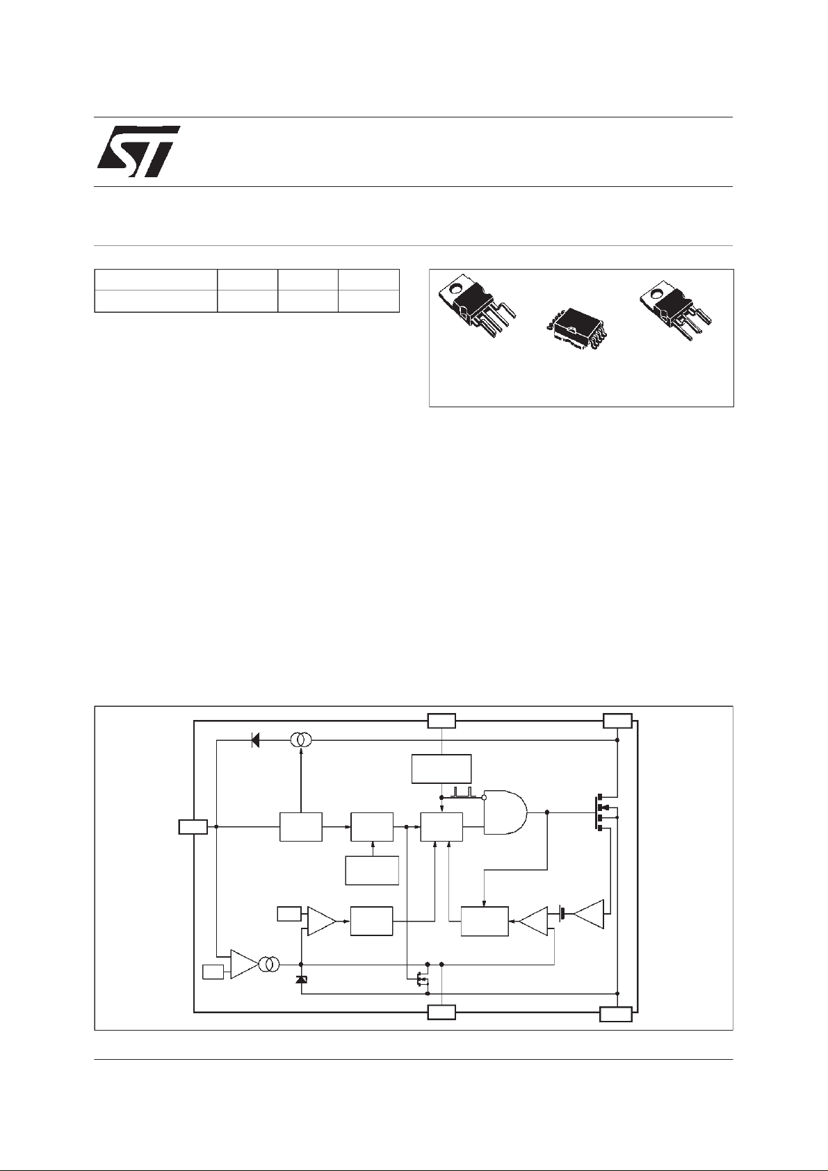
DESCRIPTION
VIPer100B/100BSP, made using VIPower M0
Technology, combines on the samesiliconchip a
state-of-the-art PWM circuit together with an
optimized high voltageavalanche rugged Vertical
Power MOSFET (400 V / 6 A). Typical
applications cover off line power supplies with
a secondary power capability of 100 W in a US
mains lines configuration. It is compatible from
both primaryor secondaryregulationloop despite
using around 50% less components when
compared with a discrete solution. Burst mode
operation is an additional feature of this device,
offering the possibility to operate in stand-by
mode without extra components.
1
(022Y)
BLOCK DIAGRAM
DD
V
January 2000
13 V
ERROR
AMPLIFIER
_
+
UVLO
LOGIC
0.5 V +
ON/OFF
_
4.5 V
SECURITY
LATCH
FF
Q
R/S
S
OVERTEMP.
DETECTOR
s
µ
1.7
DELAY
OSC
OSCILLATOR
PWM
LATCH
S
R1
FF
R2 R3
COMP
Q
250 ns
BLANKING
0.5V
+
_
_
+
CURRENT
AMPLIFIER
0.5V/A
DRAIN
SOURCE
1
3
2
0
0
C
F
1/20
VIPER100B/BSP
ABSOLUTEMAXIMUM RATING
Symbol Para met e r Val u e Uni t
V
I
V
V
OSC
V
COMP
I
COMP
V
I
D(AR)
P
T
T
THERMALDATA
R
thj-case
R
thj-a mb.
(*) When mounted using the minimum recommended pad size on FR-4 board.
Continuous Dr ain -S ou r ce Voltage (Tj = 25 to 125oC) -0.3 to 400 V
DS
Maximum Current Internally Limited A
D
Supply Volt age 0 to 15 V
DD
Volt a ge Range Input 0 to V
DD
Volt a ge Range Input 0 t o 5 V
Maximum Continuous Current ±2mA
Electrostatic d ischarge (R = 1.5 KΩ C = 100p F )
esd
Avalanche Drain-Source Current , Repetiti ve or No t-R epetitiv e
=100oC, Pulse Width Limite d by TJmax, δ <1%)
(T
C
Power Dissi pation at T c = 25oC82W
tot
Junction Oper ating Tempera tu r e Int er na lly Lim it e d
j
St orage Temperat u r e -65 to 15 0
stg
4000 V
3A
PENTAWATT-HV PowerSO-10(*)
Ther mal Resistanc e Junction-c a se Max 1.4 1.4
Ther mal Resistanc e Am bi ent-case Max 60 50
o
o
o
C/W
o
C/W
V
C
C
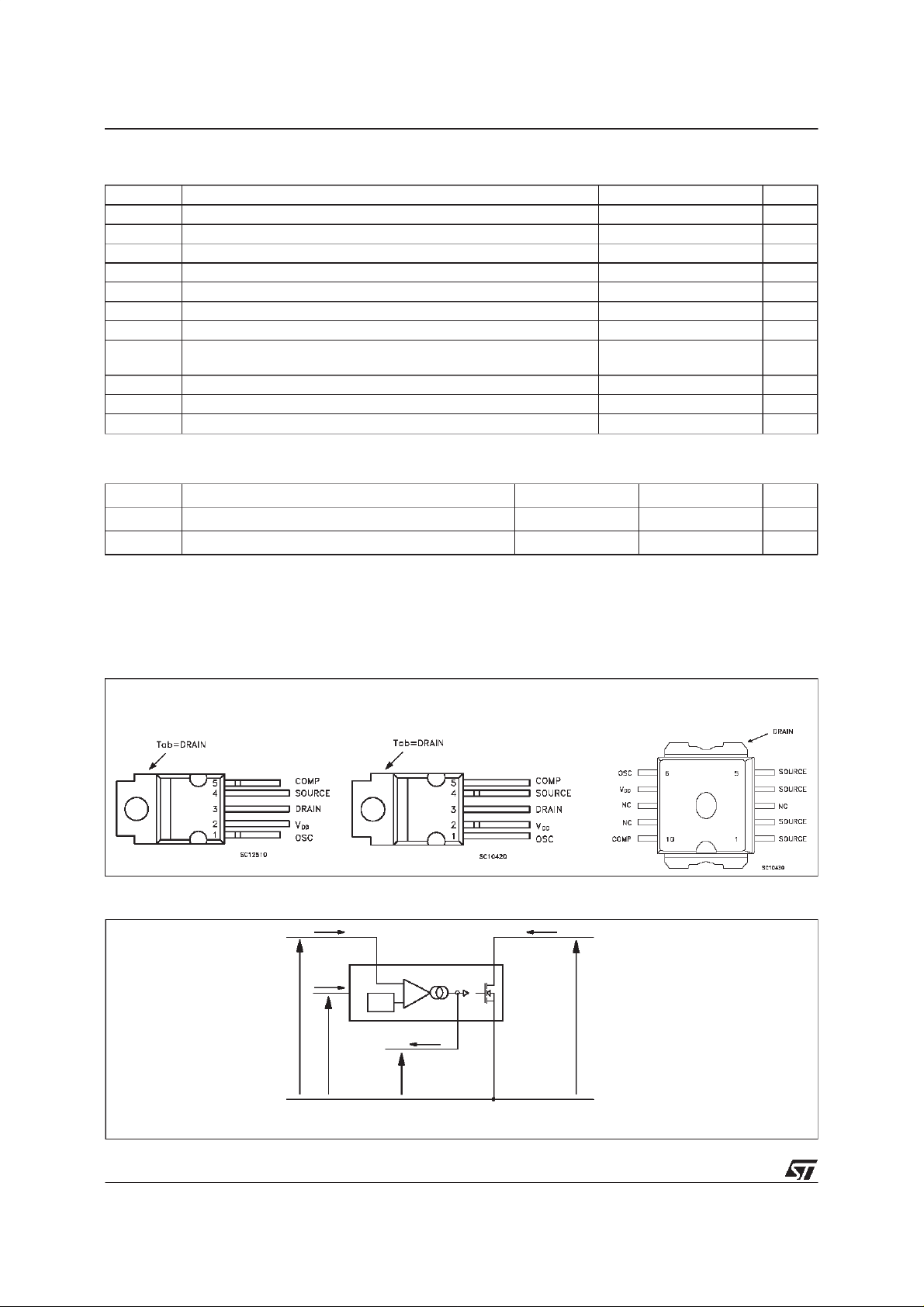
CONNECTION DIAGRAMS(Top View)
PENTAWATTHV PENTAWATTHV (022Y) PowerSO-10
CURRENT AND VOLTAGE CONVENTIONS
IDD ID
OSC
I
OSC
DD
V
13V
OSC
V
+
ICOMP
VCOMP
DRAINVDD
COMP SOURCE
VDS
2/20
FC00020

ORDERING NUMBERS
PENTAW AT T HV PENT AWAT T HV (0 22Y) Pow erSO-10
VIP er 1 00B VIPe r 10 0B (0 22Y) VIPe r 100 B SP
VIPER100B/BSP
PINSFUNCTIONAL DESCRIPTION
DRAINPIN:
Integrated power MOSFET drain pin. It provides
internal bias current during start-up via an
integrated high voltage current source which is
switched off during normal operation.The device
is able to handle an unclamped current during its
normal operation, assuring self protection against
voltage surges, PCB stray inductance, and
allowing a snubberless operation for low output
power.
SOURCEPIN:
Power MOSFET source pin. Primary side circuit
commongroundconnection.
VDD PIN :
This pin providestwo functions:
- It corresponds to the low voltage supply of the
controlpart of the circuit. If V
the start-up current source is activatedand the
output power MOSFET is switched off untilthe
voltage reaches 11V. During this phase,
V
DD
the internal current consumption is reduced,
the V
pin is sourcing a currentof about 2mA
DD
and the COMP pin is shorted to ground. After
that, the current source is shut down, and the
devicetries to startup by switchingagain.
goes below 8V,
DD
- Thispin isalso connectedto the error amplifier,
in order to allow primary as well as secondary
regulation configurations. In case of primary
regulation, an internal 13V trimmed reference
voltage is used to maintain V
secondary regulation, a voltage between 8.5V
and 12.5V will be put on V
transformerdesign, in orderto stuckthe output
of the transconductance amplifier to the high
state. The COMP pin behaves as a constant
at 13V. For
DD
DD
pin by
current source, and can easily be connectedto
the output of an optocoupler. Note that any
overvoltage due toregulation loop failure is still
detected by the error amplifier through the V
DD
voltage, which cannot overpass 13V. The
output voltage will be somewhat higher than
the nominalone, but still under control.
COMP PIN :
This pin provides two functions :
- It is the output of the error transconductance
amplifier, and allows for the connection of a
compensation network to provide the desired
transfer function of the regulation loop. Its
bandwidth can be easily adjusted to the
needed value withusual componentsvalue. As
stated above, secondary regulation
configurations are also implemented through
the COMP pin.
- When the COMP voltage is going below 0.5V,
the shut-downof the circuit occurs, with a zero
duty cycle for the power MOSFET.This feature
can be used to switch off the converter, and is
automatically activated by the regulation loop
(whatever is the configuration) to provide a
burst mode operation in case of negligible
output power or openload condition.
OSC PIN :
An R
to define the switching frequency. Note that
despite the connection of R
significant frequency change occurs for V
varying from 8V to 15V. It provides also a
synchronisationcapability, when connectedto an
external frequencysource.
network must be connected on that pin
T-CT
to VDD,no
T
DD
3/20
VIPER100B/BSP
AVALANCHE CHARACTERISTICS
Symbol Para met e r Max Valu e Uni t
I
D(ar)
E
Avalanche Curre nt , Rep et itive or Not - Re petitive
(pulse width limited by T
Single Pulse Avalanche Energy
(ar)
(starting T
=25oC, ID=I
j
max, δ <1%)
j
) (see fig.12)
D(ar)
ELECTRICAL CHARACTERISTICS (TJ=25oC, VDD=13 V, unless otherwise specified)
POWERSECTION
Symbol Pa ram et e r Test Con d i ti ons Mi n . Typ . Ma x. Unit
BV
I
DSS
R
DS(on)
C
OSS
(1) On Inductive Load, Clamped.
Drain-Source Voltage ID=1mA V
DSS
Off -St ate Drain Current V
St at i c Drain Source o n
Resistance
t
Fall Time ID=0.2AVin= 3 00 V ( 1)
f
=0V TJ= 125oC
COMP
=400V 1 mA
V
DS
ID=4A
=4A TJ=100oC
I
D
= 0 V 400 V
COMP
(see fig.3)
Rise Tim e ID=4A Vin= 3 00 V ( 1)
t
r
(see fig. 3)
Out put Capacitance VDS= 2 5 V 180 pF
3A
60 mJ
0.9 1.1
2
100 ns
50 ns
Ω
Ω
SUPPLY SECTION
Symbol Pa ram et e r Test Co nditi ons Mi n . Typ . Ma x. Uni t
I
DDch
I
DD0
I
DD1
I
DD2
V
DDo f f
V
DDo n
V
DDhyst
St art-up C ha r ging
Current
Oper ating Supply C ur rent VDD=12V, FSW=0KHz
VDD=5V VDS=70V
(see fig. 2 and fig. 15)
-2 mA
12 16 mA
(see fig. 2)
Oper ating Supply C ur rent VDD=12V, FSW= 1 00 K Hz 15.5 mA
Oper ating Supply C ur rent VDD=12V, FSW=200KHz 19 mA
Unde rv oltage Shut down (see f i g. 2) 8 V
Unde rv oltage Reset (se e fig. 2) 11 12 V
Hyst eresis Start-up (see f i g. 2) 2.4 3 V
4/20
VIPER100B/BSP
ELECTRICAL CHARACTERISTICS (continued)
OSCILLATORSECTION
Symbol Pa ram et e r Test Co nditi ons Mi n . Typ . Ma x. Uni t
F
V
OSCih
V
OSCil
ERRORAMPLIFIERSECTION
Symbol Parameter Test Cond itions Min. Typ. Max. Unit
V
DDre
∆V
DDreg
G
A
VOL
G
V
COMPLO
V
COMPHI
I
COMPLO
I
COMPHI
Os cillator Fr equ ency
SW
Total Variation
=8.2K
R
T
=9to15V
V
DD
with R
Ω
CT=2.4 nF
± 1% CT ± 5%
T
90 100 110 KHz
(see fig. 6 and fig. 9)
Os cillator Peak Voltage 7.1 V
Os cillator Valley Voltage 3. 7 V
Vg Regul at i on Point I
=0mA(seefig.1) 12.61313.4 V
COMP
Total Variation TJ= 0 to 100oC2%
Unity Gain B a ndwidth From Input = VDDto Output = V
BW
COMP
150 KHz
COM P pi n is open (see f ig. 10)
Open Loop Volt age
COM P pi n is open (see f ig. 10) 45 52 dB
Gain
DC Transc o nductance V
m
Out put Low Level
Out put High Level
Out put Low Curr ent
= 2.5 V (see fig. 1) 1.1 1.5 1.9 mA/V
COMP
=-400µAVDD=14V
I
COMP
=400µAVDD=12V
I
COMP
V
=2.5V VDD=14V -600 µA
COMP
0.2 V
4.5 V
Capa bility
Output High Current
V
=2.5V VDD= 1 2 V 600 µA
COMP
Capa bility
PWM COMPARATOR SECTION
Symbol Parameter Test Cond itions Min. Typ. Max. Unit
H
ID ∆V
V
COMPoffVCOMP
I
Dpeak
t
Peak Curr ent Limitation VDD= 1 2 V COMP pin open 6 8 11 A
Current Sense Delay
d
/∆I
COMP
Dpeak
offset I
V
= 1 t o 3 V 0.35 0.5 0.65 V/A
COMP
=10mA 0.5 V
Dpeak
ID= 1 A 250 ns
to turn-off
t
t
on(min)
Blanking Time 250 360 ns
b
Minimum on T ime 350 ns
SHUTDOWNAND OVERTEMPERATURE SECTION
Symbol Parameter Test Cond itions Min. Typ. Max. Unit
V
COMPth
t
DISsu
T
T
hyst
Restart threshold (see fig. 4) 0.5 V
Disabl e Set Up Tim e (see fig. 4) 1.7 5 µs
Thermal Shutdown
tsd
(see fig. 8) 140 170
Tem p er at u re
Thermal Shutdown
(see fig. 8) 40
Hyst e r esis
o
o
C
C
5/20
VIPER100B/BSP
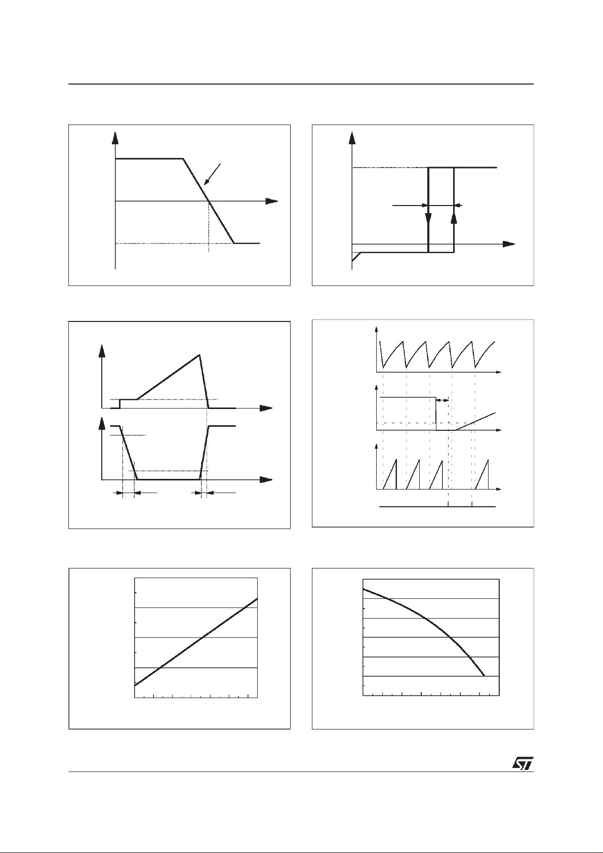
Figure1:VDDRegulationPoint
COMP
I
ICOMPHI
0
ICOMPLO
VDDreg
Figure3: TransitionTime
ID
10%Ipeak
Slope =
Gm in mA/V
FC00150
Figure2: UndervoltageLockout
IDD
IDD0
DD
V
VDDhyst
V
DDoff
IDDch
Figure4: ShutDown Action
VOSC
VCOMP
t
tDISsu
VDS=70V
Fsw = 0
V
DDon
FC00170
VDD
t
VDS
VCOMPth
90%VD
ID
10%V
D
t
tf tr
FC00160
ENABLE
DISABLE
Figure5: BreakdownVoltage vs Temperature Figure 6: Typical FrequencyVariation
1.15
BV
DS S
(Nor malize d)
1.1
1.05
0.95
1
0 20406080100120
Temperature ( C)
FC00180
1
(%)
0
-1
-2
-3
-4
-5
0 20 40 60 80 100 120 140
Temperature ( C)
t
t
ENABLE
FC00060
FC00190
6/20
 Loading...