

SGS Thomson Microelectronics UC3845AN, UC3844AN, UC3843AN, UC3845AD, UC3844AD Datasheet
...
UC2842A/3A/4A/5A
UC3842A/3A/4A/5A
HIGH PERFORMANCE CURRENTMODE PWM CONTROLLER
TRIMMED OSCILLATOR DISCHARGE CUR-
.
RENT
CURRENT MODEOPERATIONTO500kHz
.
AUTOMATIC FEED FORWARD COMPENSA-
.
TION
LATCHING PWM FOR CYCLE-BY-CYCLE
.
CURRENT LIMITING
INTERNALLY TRIMMED REFERENCE WITH
.
UNDERVOLTAGELOCKOUT
HIGHCURRENTTOTEMPOLEOUTPUT
.
UNDERVOLTAGE LOCKOUT WITH HYSTER-
.
ESIS
LOWSTART-UPCURRENT (< 0.5mA)
.
DOUBLEPULSESUPPRESSION
.
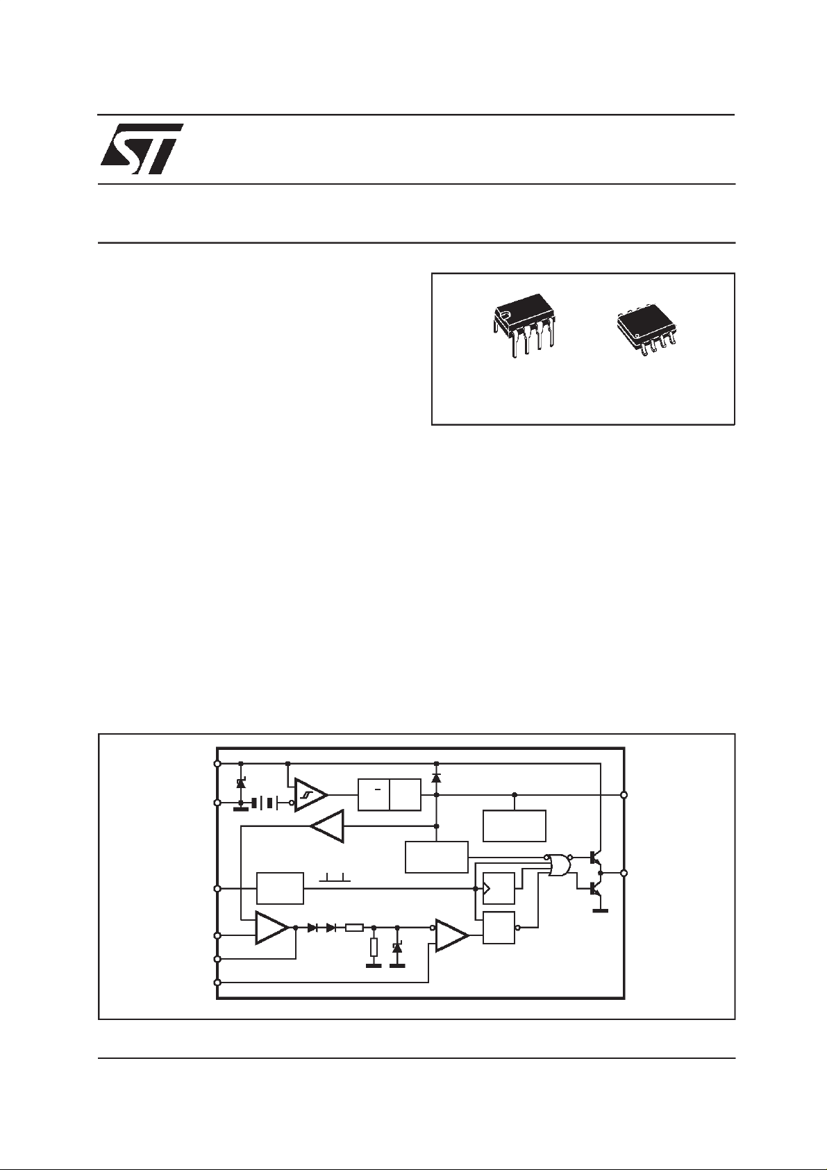
DESCRIPTION
TheUC384xAfamilyofcontrolICsprovidesthenecessaryfeaturesto implement off-lineor DC to DC
fixedfrequencycurrent modecontrolschemeswith
a minimal external parts count. Internally implementedcircuitsincludea trimmedoscillatorfor precise DUTY CYCLECONTROL under voltagelockoutfeaturingstart-upcurrentlessthan0.5mA,a precision reference trimmed for accuracyat the error
ampinput,logictoinsurelatchedoperation,a PWM
comparatorwhichalsoprovidescurrentlimit control,
and a totempole output stage designed to source
orsinkhighpeakcurrent.Theoutputstage,suitable
for driving N-Channel MOSFETs, is low in the offstate.
Differencesbetweenmembersof thisfamily arethe
under-voltagelockoutthresholdsandmaximumduty
cycle ranges. The UC3842A and UC3844A have
UVLOthresholds of 16V (on) and 10V (off), ideally
suitedoff-lineapplicationsThecorrespondingthresholds for the UC3843A and UC3845A are 8.5 V and
7.9V.The UC3842A and UC3843A can oper ateto
dutycyclesapproaching100%.Arangeofthezeroto
<50%is obtainedbytheUC3844AandUC3845Aby
theadditionofaninternaltoggleflipflopwhichblanks
theoutputoffeveryotherclockcycle.
Minidip
SO8
BLOCK DIAGRAM (toggle flip flop used only in UC3844A and UC3845A)
7
Vi
2.50V
UVLO
S/R
2R
R1V
5V
REF
VREF GOOD
LOGIC
S
R
CURRENT
SENSE
COMPARATOR
INTERNAL
BIAS
T
LATCH
UC3842A
March 1999
GROUND
RT/CT
VFB
COMP
CURRENT
SENSE
34V
5
4
2
1
3
OSC
ERROR AMP.
+
- PWM
D95IN331
8
6
VREF
5V 50mA
OUTPUT
1/15
UC2842A/3A/4A/5A - UC3842A/3A/4A/5A
ABSOLUTEMAXIMUMRATINGS
Symbol Parameter Value Unit
V
V
I
O
E
O
P
tot
P
tot
T
stg
T
J
T
L
*
Allvoltagesare with respect to pin 5, all currents arepositiveinto the specifiedterminal.
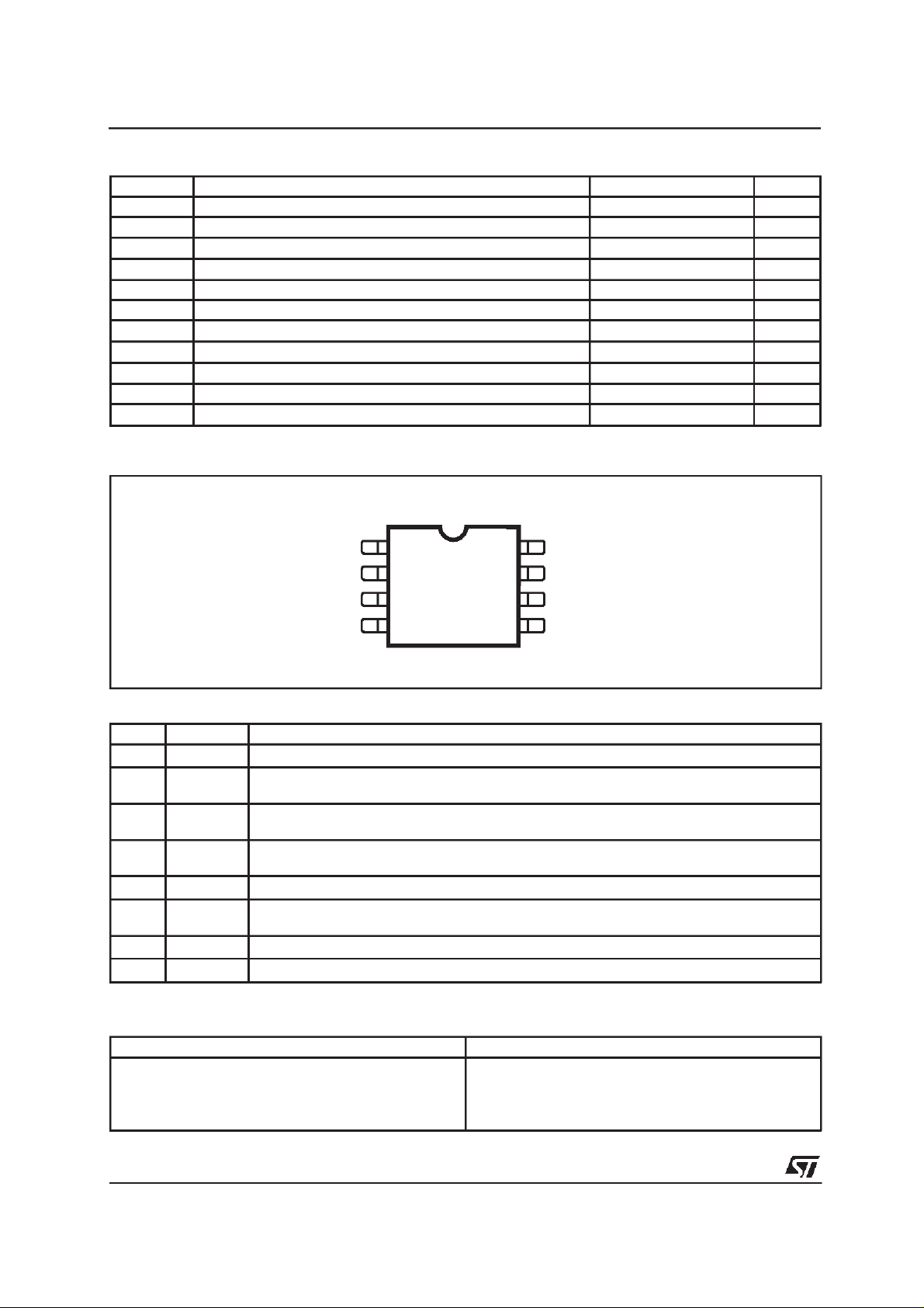
PIN CONNE C TI ON
SupplyVoltage (low impedance source) 30 V
i
SupplyVoltage (Ii < 30mA) Self Limiting
i
Output Current
1
±
Output Energy (capacitive load) 5
Analog Inputs(pins 2, 3) – 0.3to 5.5 V
ErrorAmplifier Output SinkCurrent 10 mA
Power Dissipation at T
amb
≤25°
C (Minidip)
Power Dissipation at Tamb≤25°C (SO8)
1.25 W
800 mW
Storage Temperature Range – 65 to 150
JunctionOperating Temperature – 40 to 150 °C
Lead Temperature (soldering 10s) 300
(top view)
Minid i p/ SO8
A
J
µ
C
°
C
°
COMP
V
FB
I
SENSE
RT/C
T
1
2
3
4
D95IN332
8
7
6
5
V
REF
Vi
OUTPUT
GROUND
PIN FUNCTIONS
No Function Description
1 COMP This pin is the Error Amplifier output and is made available for loop compensation.
2V
3I
4R
SENSE
T/CT
5 GROUND This pin is the combined control circuitry and power ground.
6 OUTPUT This output directly drives the gate of a power MOSFET. Peak currents up to 1A are sourced
7V
CC
8V
This is the inverting input of the Error Amplifier. It is normally connected to the switching
FB
power supply output through a resistor divider.
A voltage proportional to inductor current is connected to this input. The PWM uses this
information to terminate the output switch conduction.
The oscillator frequency and maximum Output duty cycle are programmed by connecting
resistor R
to Vref and cpacitor CTto ground. Operation to 500kHz is possible.
T
and sunk by this pin.
This pin is the positive supply of the control IC.
This is the reference output. It provides charging current for capacitor CTthrough resistor RT.
ref
ORDERINGNUMBERS
UC2842AD1; UC3842AD1
UC2843AD1; UC3843AD1
UC2844AD1; UC3844AD1
UC2845AD1; UC3845AD1
2/15
SO8 Minidip
UC2842AN; UC3842AN
UC2843AN; UC3843AN
UC2844AN; UC3844AN
UC2845AN; UC3845AN
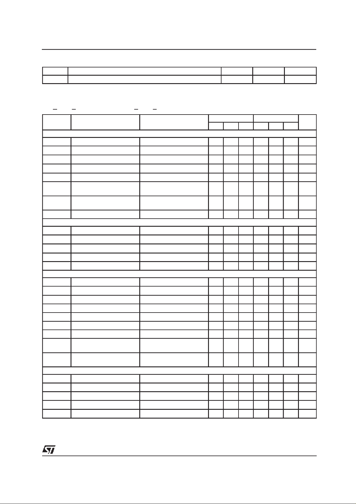
UC2842A/3A/4A/5A - UC3842A/3A/4A/5A
THERMAL DATA
Symbol Description Mi n i dip SO 8 U n it
R
th j-amb
Thermal ResistanceJunction-ambient. max. 100 150
°
C/W
ELECTRICALCHARACTERISTICS
-25 < T
<85°C forUC284XA;0 < T
amb
( [note 1] Unless otherwise stated, these specificationsapply for
<70°CforUC384XA;Vi=15V(note 5); RT= 10K; CT= 3.3nF)
amb
Symbol Parameter Test Conditions
REFERENCE SECTION
V
∆V
∆V
V
∆
REF
Output Voltage
REF
Line Regulation
REF
Load Regulation
REF
Temperature Stability (Note 2) 0.2 0.2
/∆T
=25°CIo= 1mA
T
j
12V ≤ V
1 ≤ I
i
≤ 20mA
o
≤ 25V
Total Output Variation Line, Load, Temperature 4.9 5.1 4.82 5.18 V
e
Output Noise Voltage
N
10Hz≤f≤10KHz T
(note 2)
Long Term Stability
= 125°C, 1000Hrs
T
amb
(note 2)
I
Output Short Circuit -30 -100 -180 -30 -100 -180 mA
SC
OSCILLATOR SECTION
f
f
∆
OSC
f
∆
OSC
V
I
dischg
OSC
Frequency
Frequency Change with Volt. V
/∆V
Frequency Change with Temp. T
/∆T
Oscillator Voltage Swing (peak to peak) – 1.6 – – 1.6 – V
OSC
Discharge Current (V
=2V) TJ=25°C 7.8 8.3 8.8 7.8 8.3 8.8 mA
OSC
=25°C
T
j
= 12V to 25V – 0.2 1 – 0.2 1 %
CC
A=Tlow
to T
high
ERROR AMP SECTION
V
BW Unity Gain Bandwidth T
PSRR Power Supply Rejec. Ratio
Input Voltage V
2
I
Input Bias Current VFB= 5V -0.1 -1 -0.1 -2
b
A
VOL
I
Output Sink Current VPIN2 = 2.7V V
o
I
Output Source Current VPIN2 = 2.3V V
o
V
High V
OUT
Low V
V
OUT
= 2.5V 2.45 2.50 2.55 2.42 2.50 2.58 V
PIN1
2V ≤ Vo≤ 4V
=25°C 0.7 1 0.7 1 MHz
J
12V≤V
PIN2
= 15KΩto Ground
R
L
PIN2
= 15KΩto Pin 8
R
L
≤
i
= 2.3V;
= 2.7V;
25V
PIN1
PIN1
CURRENT SENSE SECTION
G
V
SVR Supply Voltage Rejection
Gain (note 3 & 4) 2.85 3 3.15 2.85 3 3.15 V/V
V
Maximum Input Signal V
3
I
Input Bias Current -2 -10 -2 -10
b
= 5V (note 3) 0.9 1 1.1 0.9 1 1.1 V
PIN1
12≤V
25V (note 3)
≤
i
Delay to Output 150 300 150 300 ns
UC284XA UC38 4XA
Min. Typ. Max. Min. Typ. Max.
Unit
4.95 5.00 5.05 4.90 5.00 5.10 V
220 220mV
325 325mV
mV/°C
=25°C
j
50 50 µ
525 525mV
47 52 57 47 52 57 KHz
–5––5–%
µA
65 90 65 90 dB
60 70 60 70 dB
= 1.1V 2 12 2 12 mA
= 5V -0.5 -1 -0.5 -1 mA
5 6.2 5 6.2 V
0.8 1.1 0.8 1.1 V
70 70 dB
µ
V
A
3/15
UC2842A/3A/4A/5A - UC3842A/3A/4A/5A
ELECTRICAL CHARACTERISTICS
(continued)
Symbol Pa ram et er Test C o n diti o n s
OUTPUT SECTION
V
V
V
Output Low Level I
OL
Output High Level I
OH
UVLO Saturation VCC= 6V; I
OLS
t
Rise Time
r
t
Fall Time
f
= 20mA 0.1 0.4 0.1 0.4 V
SINK
I
= 200mA 1.6 2.2 1.6 2.2 V
SINK
= 20mA 13 13.5 13 13.5 V
SOURCE
I
T
T
= 200mA 12 13.5 12 13.5 V
SOURCE
= 1mA 0.7 1.2 0.7 1.2 V
SINK
=25°CCL= 1nF (2)
j
=25°CCL= 1nF (2)
j
UNDER-VOLTAGE LOCKOUT SECTION
Start Threshold X842A/4A 15 16 17 14.5 16 17.5 V
X843A/5A 7.8 8.4 9.0 7.8 8.4 9.0 V
Min Operating Voltage
After Turn-on
X842A/4A 9 10 11 8.5 10 11.5 V
X843A/5A 7.0 7.6 8.2 7.0 7.6 8.2 V
PWM SECTION
Maximum Duty Cycle X842A/3A 94 96 100 94 96 100 %
X844A/5A 47 48 50 47 48 50 %
Minimum Duty Cycle 0 0 %
TOTAL STANDBY CURRENT
I
Start-up Current Vi= 6.5V for UCX843A/45A 0.3 0.5 0.3 0.5 mA
st
V
= 14V for UCX842A/44A 0.3 0.5 0.3 0.5 mA
i
I
V
Operating Supply Current V
i
Zener Voltage Ii= 25mA 30 36 30 36 V
iz
PIN2=VPIN3
=0V 12 17 12 17 mA
UC284X A UC384 X A
Min. Typ. Max. Min. Typ. Max.
50 150 50 150 ns
50 150 50 150 ns
Unit
Notes : 1. Max package power dissipation limitsmust be respected; low duty cycle pulse techniquesare used duringtestmaintainTjas
close to T
2. Theseparameters, although guaranteed, are not100%testedin production.
3. Parametermeasured at trippointof latchwithV
4. Gain definedas :
A= ;0≤V
5. AdjustViabovethestart threshold before setting at 15 V.
∆ V
∆ V
aspossible.
amb
PIN1
PIN3
PIN3
≤
0.8V
PIN2
=0.
4/15
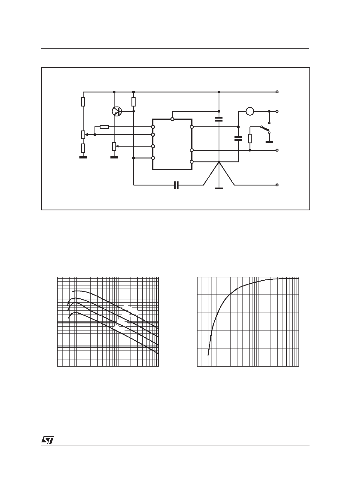
Figure1: OpenLoop Test Circuit.
4.7KΩ
UC2842A/3A/4A/5A - UC3842A/3A/4A/5A
V
REF
R
T
V
REF
ERROR AMP.
ADJUST
4.7KΩ
1KΩ
100KΩ
I
SENSE
ADJUST
D95IN343
5KΩ
COMP
V
I
SENSE
RT/C
FB
T
1
2
UC3842A
3
4
Highpeakcurrentsassociatedwithcapacitiveloads
necessitate careful grounding techniques. Timing
and bypass capacitorsshould be connectedclose
Figure 2:
Oscillator Frequency vs Timing Resistance
f
(Hz)
o
D96IN362
A2N2222
7
6
5
0.1µF
V
i
OUTPUT
GROUND
0.1µF
1W
1KΩ
8
C
T
V
i
OUTPUT
GROUND
to pin 5 ina singlepointground.The transistorand
5KΩpotentiometerareusedtosampletheoscillator
waveformand applyan adjustablerampto pin 3.
Figure 3:
Maximum Duty Cycle vs Timing Resistor
f
o
(Hz)
D96IN363
1M
CT=470pF
1nF
100K
10K
1K
300 1K 3K 10K 30K RT(Ω)
2.2nF
4.7nF
80
60
40
20
0
300 1K 3K 10K 30K RT(Ω)
5/15
 Loading...