

SGS Thomson Microelectronics UC3845N, UC3845D, UC3843D, UC3844D, UC3844N Datasheet
...
UC2842/3/4/5
CURRENTMODEPWMCONTROLLER
OPTIMIZED FOR OFF-LINE AND DC TO DC
.
CONVERTERS
LOWSTART-UP CURRENT(< 1 mA)
.
AUTOMATIC FEED FORWARD COMPENSA-
.
TION
PULSE-BY-PULSECURRENT LIMITING
.
ENHANCED LOAD RESPONSE CHARAC-
.
TERISTICS
UNDER-VOLTAGELOCKOUTWITHHYSTER-
.
ESIS
DOUBLEPULSESUPPRESSION
.
HIGHCURRENT TOTEMPOLEOUTPUT
.
INTERNALLY TRIMMED BANDGAP REFER-
.
ENCE
500 KHz OPERATION
.
LOWROERRORAMP
.
DESCRIPTION
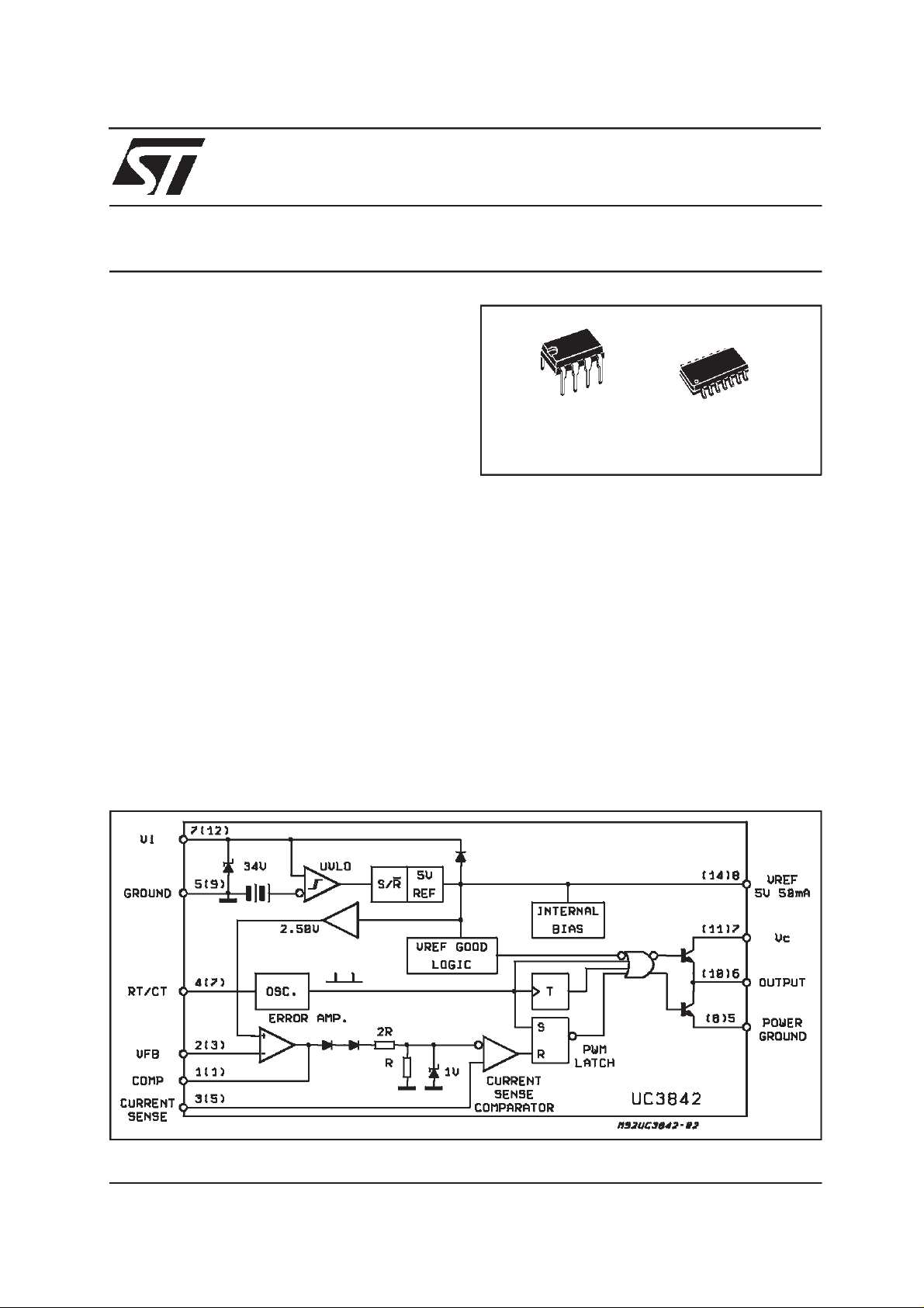
TheUC3842/3/4/5familyofcontrolICsprovidesthe
necessaryfeatures to implement off-line or DC to
DC fixed frequencycurrentmode controlschemes
witha minimalexternalpartscount.Internallyimplementedcircuitsincludeundervoltagelockoutfeaturingstart-upcurrent less than 1 mA,a precisionreferencetrimmedforaccuracyattheerrorampinput,
UC3842/3/4/5
Minidip
logicto insurelatchedoperation,a PWMcomparatorwhichalsoprovidescurrentlimitcontrol,andatotem pole output stage designed to source or sink
high peak current. The output stage, suitable for
drivingN-ChannelMOSFETs,islowintheoff-state.
Differencesbetweenmembersofthisfamilyarethe
under-voltage lockout thresholds and maximum
dutycycle ranges.The UC3842 and UC3844have
UVLOthresholdsof 16V (on) and 10V (off),ideally
suited off-line applications The corresponding
thresholdsfor the UC3843 and UC3845 are 8.5 V
and 7.9 V. The UC3842 and UC3843 can operate
to duty cycles approaching 100%. A range of the
zero to < 50 % is obtained by the UC3844 and
UC3845bytheadditionof aninternaltoggleflipflop
whichblanksthe outputoff every otherclockcycle.
SO14
BLOCK DIAGRAM (togg le flip flop used only in U3844 and UC3845)
October1998
1/11
UC2842/3/4/5-UC3842/3/4/5
ABSOLUTEMAXIMUMRATINGS
Symbol Parameter Value Unit
V
i
V
i
I
O
E
O
P
tot
P
tot
T
stg
T
L
*
All voltages are withrespect to pin 5, all currents are positiveinto the specifiedterminal.
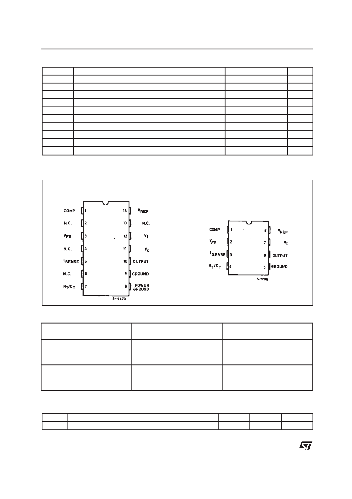
PIN CONNECTI O NS ( top views)
SupplyVoltage(low impedance source) 30 V
SupplyVoltage(Ii < 30mA) SelfLimiting
Output Current
1
±
Output Energy (capacitive load) 5
Analog Inputs (pins 2, 3) – 0.3 to 6.3 V
ErrorAmplifierOutput SinkCurrent 10 mA
Power Dissipationat T
≤ 50 °C (minidip, DIP-14)
amb
Power Dissipationat Tamb ≤ 25°C (SO14)
1W
725 mW
Storage Temperature Range – 65 to 150
Lead Temperature (soldering 10s) 300
SO1 4 Minidip
µ
°C
°C
A
J
ORDERING NUMBERS
Type Minidip SO14
UC2842
UC3843
UC2844
UC2845
UC3842
UC3843
UC3844
UC3845
UC2842N
UC2843N
UC2844N
UC2845N
UC3842N
UC3843N
UC3844N
UC3845N
UC2842D
UC2843D
UC2844D
UC2845D
UC3842D
UC3843D
UC3844D
UC3845D
THERMAL DATA
Symb o l Description Minidi p SO 14 Unit
R
2/11
thj-amb
Thermal ResistanceJunction-ambient. max. 100 165
C
°
UC2842/3/4/5-UC3842/3/4/5
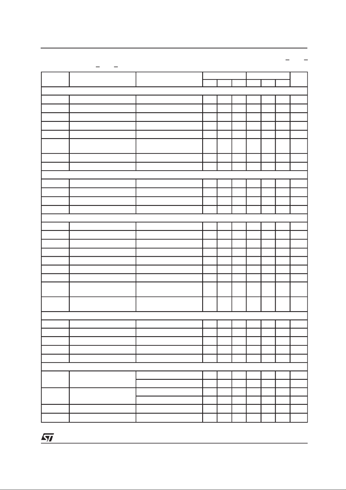
ELECTRICAL CHARACTERISTICS
85°C for UC2824X;0 < T
Symb ol Parameter Test Conditi o ns
<70°CforUC384X;Vi=15V(note5); RT= 10K; CT= 3.3nF)
amb
(Unlessotherwise stated,these specificationsapply for -25 < T
UC284X UC384X
Min. T yp. Max. Min. Typ. Max.
REFERENCE SECTION
V
REF
V
∆
REF
V
∆
REF
∆V
REF
/∆T
Output Voltage
Line Regulation
Load Regulation
=25°CIo= 1mA
T
j
12V≤V
1≤I
o
i
≤
≤
20mA
25V
Temperature Stability (Note 2) 0.2 0.4 0.2 0.4
4.95 5.00 5.05 4.90 5.00 5.10 V
620 620mV
625 625mV
Total Output Variant Line, Load, Temperature (2) 4.9 5.1 4.82 5.18 V
e
N
Output Noise Voltage
10Hz ≤ f ≤ 10KHz T
=25°C
j
50 50
(2)
I
SC
Long Term Stability
T
= 125°C, 1000Hrs (2)
amb
Output Short Circuit -30 -100 -180 -30 -100 -180 mA
525 525mV
OSCILLATOR SECTION
f
s
Initial Accuracy
Voltage Stability
Temperature Stability
V
4
Amplitude V
=25°C (6)
T
j
T
MIN
12≤V
≤
PIN4
25V
≤
i
T
T
(2)
≤
amb
MAX
Peak to Peak 1.7 1.7 V
47 52 57 47 52 57 KHz
0.2 1 0.2 1 %
55%
ERROR AMP SECTION
V
2
I
b
Input Voltage V
= 2.5V 2.45 2.50 2.55 2.42 2.50 2.58 V
PIN1
Input Bias Current -0.3 -1 -0.3 -2
A
VOL
2≤V
4V
≤
o
65 90 65 90 dB
B Unity Gain Bandwidth (2) 0.7 1 0.7 1 MHz
SVR Supply Voltage Rejection
I
o
I
o
Output Sink Current V
Output Source Current V
V
High V
OUT
V
Low V
OUT
12V≤V
= 2.7V V
PIN2
= 2.3V V
PIN2
= 2.3V;
PIN2
= 15KΩto Ground
R
L
= 2.7V;
PIN2
= 15KΩto Pin 8
R
L
25V
≤
i
= 1.1V 2 6 2 6 V
PIN1
= 5V -0.5 -0.8 -0.5 -0.8 mA
PIN1
60 70 60 70 dB
56 56 V
0.7 1.1 0.7 1.1 V
CURRENT SENSE SECTION
G
V
V
3
Maximum Input Signal V
SVR Supply Voltage Rejection
I
b
Gain (3 & 4) 2.85 3 3.15 2.8 3 3.2 V/V
= 5V (3) 0.9 1 1.1 0.9 1 1.1 V
PIN1
12≤V
≤
i
25V (3)
70 70 dB
Input Bias Current -2 -10 -2 -10 µ
Delay to Output 150 300 150 300 ns
OUTPUT SECTION
I
OL
I
OH
t
r
t
f
Output Low Level I
= 20mA 0.1 0.4 0.1 0.4 V
SINK
I
= 200mA 1.5 2.2 1.5 2.2 V
SINK
Output High Level ISOURCE = 20mA 13 13.5 13 13.5 V
Rise Time
Fall Time
I
=25°CCL= 1nF (2)
T
j
=25°CCL= 1nF (2)
T
j
= 200mA 12 13.5 12 13.5 V
SOURCE
50 150 50 150 ns
50 150 50 150 ns
amb
Unit
mV/°C
µV
A
µ
A
<
3/11
UC2842/3/4/5-UC3842/3/4/5
ELECTRICAL CHARACTERISTICS
(continued)
Symbol Parameter Test Conditi o ns
UNDER-VOLTAGE LOCKOUT SECTION
Start Threshold X842/4 15 16 17 14.5 16 17.5 V
X843/5 7.8 8.4 9.0 7.8 8.4 9 V
Min Operating Voltage
After Turn-on
X842/4 9 10 11 8.5 10 11.5 V
X843/5 7.0 7.6 8.2 7.0 7.6 8.2 V
PWM SECTION
Maximum Duty Cycle X842/3 93 97 100 93 97 100 %
X844/5 46 48 50 47 48 50 %
Minimum Duty Cycle 0 0 %
TOTAL STANDBY CURRENT
I
st
I
i
V
iz
Notes : 2. These parameters, although guaranteed, arenot 100% testedin production.
3. Parameter measured at trippoint of latchwith V
4. Gain defined as :
A= ;0≤V
5. Adjust Viabovethe startthreshold before settingat 15 V.
6. Output frequency equals oscillator frequency for the UC3842and UC3843.
Outputfrequency is one halfoscillator frequency for the UC3844and UC3845.
Start-up Current 0.5 1 0.5 1 mA
Operating Supply Current V
PIN2=VPIN3
=0V 11 20 11 20 mA
Zener Voltage Ii= 25mA 34 34 V
=0.
PIN2
∆ V
∆ V
PIN1
PIN3
PIN3
≤
0.8V
UC284X UC384X
Min. T yp. Max. Min. T yp. Max.
Unit
4/11
 Loading...