

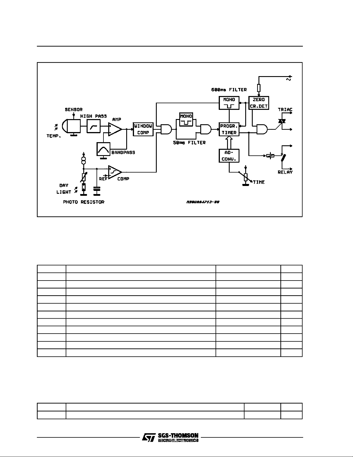
MOTION DETECTOR INTERFACE
50/ 60Hz ACSUPPLY
INPUTFORPYROELECTRICALSENSOR
INPUTFORPHOTORESISTIVE SENSOR
SENSORFILTER AMPLIFIER
PROGRAMMABLEON-TIMER
TRIACOUTPUTANDRELAYOUTPUT
SHORTCIRCUIT PROTECTION
LOW QUIESCENTCURRENT
TWO-WIRE TECHNIQUE
DESCRIPTION
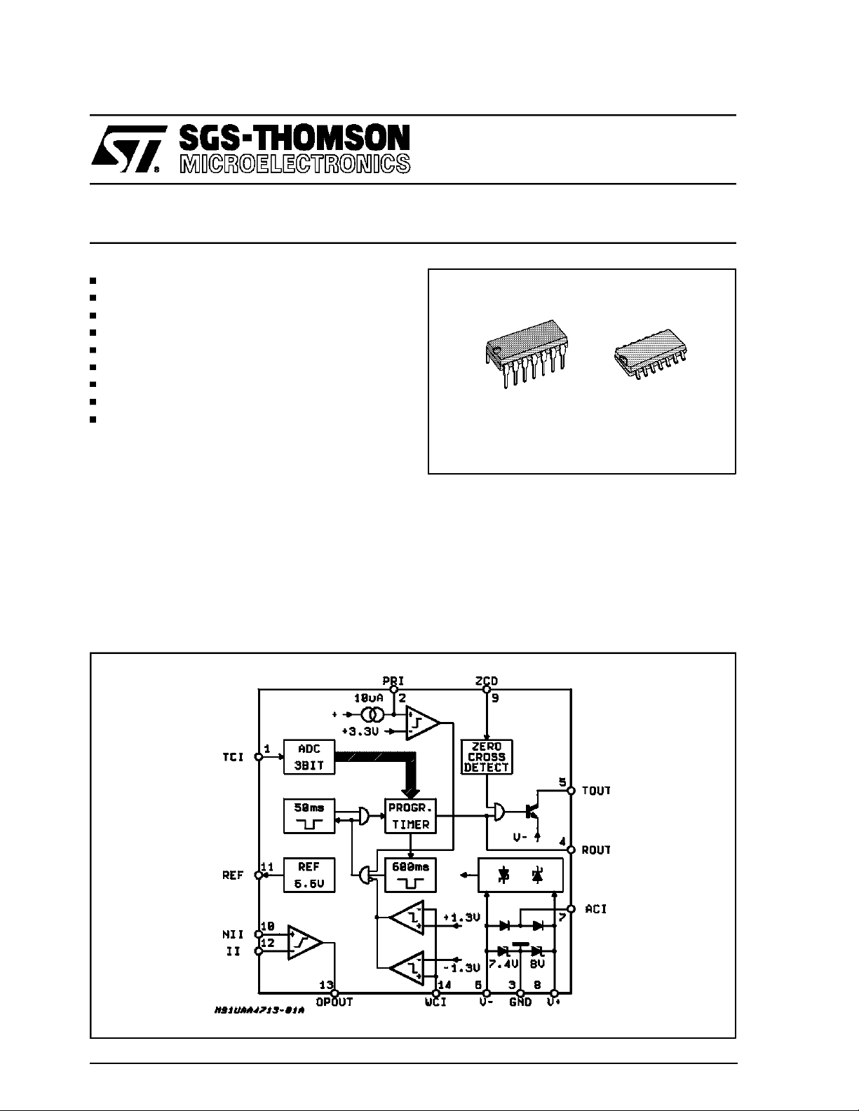
The UAA4713 is a monolithicintegrated circuit intended to control triac or relay switch for ACmains timer applications.Thedevice can be used
in a wide range of industrial and consumer applications as light control, automatic door opening
detector, fire alarm, fluid level control .
The circuit processes the output signal of an infrared pyroelectric detector which senses temperature changes caused by heat radiation of the humanbody.
UAA4713
ADVANCE DATA
DIP-14 SO-14
ORDERING NUMBERS:
UAA4713DP UAA4713FP
If the sensor detects a temperature change, a
programmable timer will start and switch a lamp
or other loads to themains.
A further input for a photo-resistivesensor allows
to program circuit operation depending on the
day-lightintensity.
Internal circuits avoid false triggering of the external actuators. (see functional diagram).
BLOCK DIAGRAM
December 1991
This is advanced information on a new product now in development or undergoing evaluation. Details are subject to change without notice.
1/14
UAA4713
FUNCTIONAL DIAGRAM
ABSOLUTE MAXIMUM RATINGS
Symbol Parameter Test Conditions Unit
I7 AC Supply Current 60 mA
I7 Peak Current (T.P < 200µs) 200 mA
I7 Sourge Current (not repetitive 10ms) 500 mA
I9 ZCD Max. Input Current 5 mA
V6-3 Negative Clamp Voltage -9 V
V8-3 Positive Clamp Voltage 9.5 V
V14-3 Comp. Input Voltage ±8V
V10-12 Differential Input Voltage ±8V
Top Operating Temperature -25to 85 °C
T
stg,Tj
P
Junction and Storage Temperature -40 to 150 °C
Total Power Dissipation (Tj=85°C) 650 mW
tot
THERMAL DATA
Symbol Parameter Value Unit
R
th j-amb
Thermal Resistance Junction-ambient max 100 °C/W
2/14
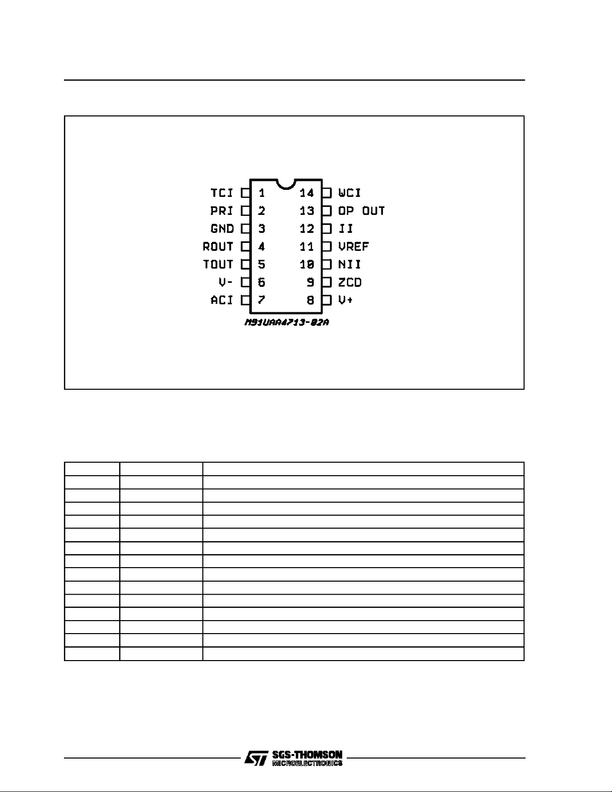
PIN CONNECTION (Top view)
UAA4713
PIN FUNCTIONS
Pin Symbols Functions
1 TCI Time control Input
2 PRI Photosensorcomparator input
3 GND Ground
4R
5T
OUT
OUT
6 V- Negative clamp voltage
7 ACI AC-inputsupply
8 V+ Positive clamp voltage
9 ZCD Zero cross detector
10 NII Non-invertinput sensor amplifier
11 V
REF
12 II Invert input sensor amplifier
13 OP OUT Output sensor amplifier
14 WCI Window comparator input
Relay output
Triac output
Sensor reference voltage
3/14
UAA4713
ELECTRICAL CHARACTERISTICS (IS= + 2mA to +10mA;T
=25°Cunless otherwise specified)
amb
Symbol Parameter Test Condition Pin Min. Typ. Max. Unit
I
V- Negative Clamping Voltage ±I
Operative Supply Current 7 ±0.7 + 15 mA
S
= 0.7mA 6 -7.8 -7 V
S
V+ Positive Clamping Voltage 8 7.6 8.4 V
V
I
ROUT
V
R HIGH
REF
Sensor Reference Voltage I
Output CurrentRelay Driver during on-time V
Relay Driver Source
=50µA
REF
I
= 200µA
REF
=0V 4 80 µA
ROUT
I
=80µA4 2V
R OUT
11 6
5
7.2
6.6 7.2
Saturation Voltage
I
R
I
TOUT
V
ZCD
Relay Sink Output Current V
= 0.4V during on-time 4 1 8 mA
R OUT
Triac Firing Current 5 50 65 mA
Zero Cross Detector
9 ±7.4 ±8 ±8.6 V
Clamping Voltage
I
ZCD
Zero Cross Detector
9 1.6 10 µA
Operating Current
I
PRI
Photoresistor Source
V
=0V 2 6 10 14 µA
PRI
Current
V
PRth
Photoresistor Threshold
IS= 0.7mA 2 3 3.3 3.6 V
Voltage
I
t
TCI
TIM
Timer ControlInput Current V
On-Timer Counter Duration
(depends on the mains
frequency and on externally
adjustable Timer Control
Input Voltage)+ 1/2 cicle
precision
0 to V+ 1 0 0.5 µA
TCI
V
TCI
14/4 50 60 Hz
11/12 V+ 0 0 s
9/12 V+ 4.48 3.73 s
7/12 V+ 40 33.3 s
5/12 V+ 81 67.5 s
3/12 V+ 163 135.8 s
1/12 V+ 327 272.5 s
0V (GND) Continue
t
D
Delay Time Between
50Hz 14/4 40 50 60 ms
Window ComparatorInput
and Timer Start
60Hz 33.3 41.6 50 ms
t
DR
Delay Time Between Timer
50Hz 14/4 500 ms
Stop to Retrigger
60Hz 600 ms
I
V
I
TOL
th WCI
WCI
TriacOutputLeakage Current VTO=0V 5 10 µA
Window ComparatorT4 Pin 2 open 14/4 ±1.20 ±1.3 ±1.40 V
Window ComparatorInput
V
= -2V to + 2V 14 ± 1 mA
WCI
Current
OP. AMP.
R
I
IO
I
IB
V
V
CM
V
I
O
I
SC
G
Input Resistance 10/12 1 MΩ
I
Input Offset Current 10/12 25 nA
Input Bias Current 10/12 1 µA
Input Offset Voltage 10/12 - 10 +10 mV
IO
Common Mode Volt. Renge 10/12 - 4.5 5 V
Output Voltage Swing 13 ±4 ±5V
O
Output Current 13 1.5 mA
Output Short Circuit Current 13 3 mA
Large SignalOpen Loop
V
RL= 10K 80 100 V
Voltage Gain
V
V
4/14
UAA4713
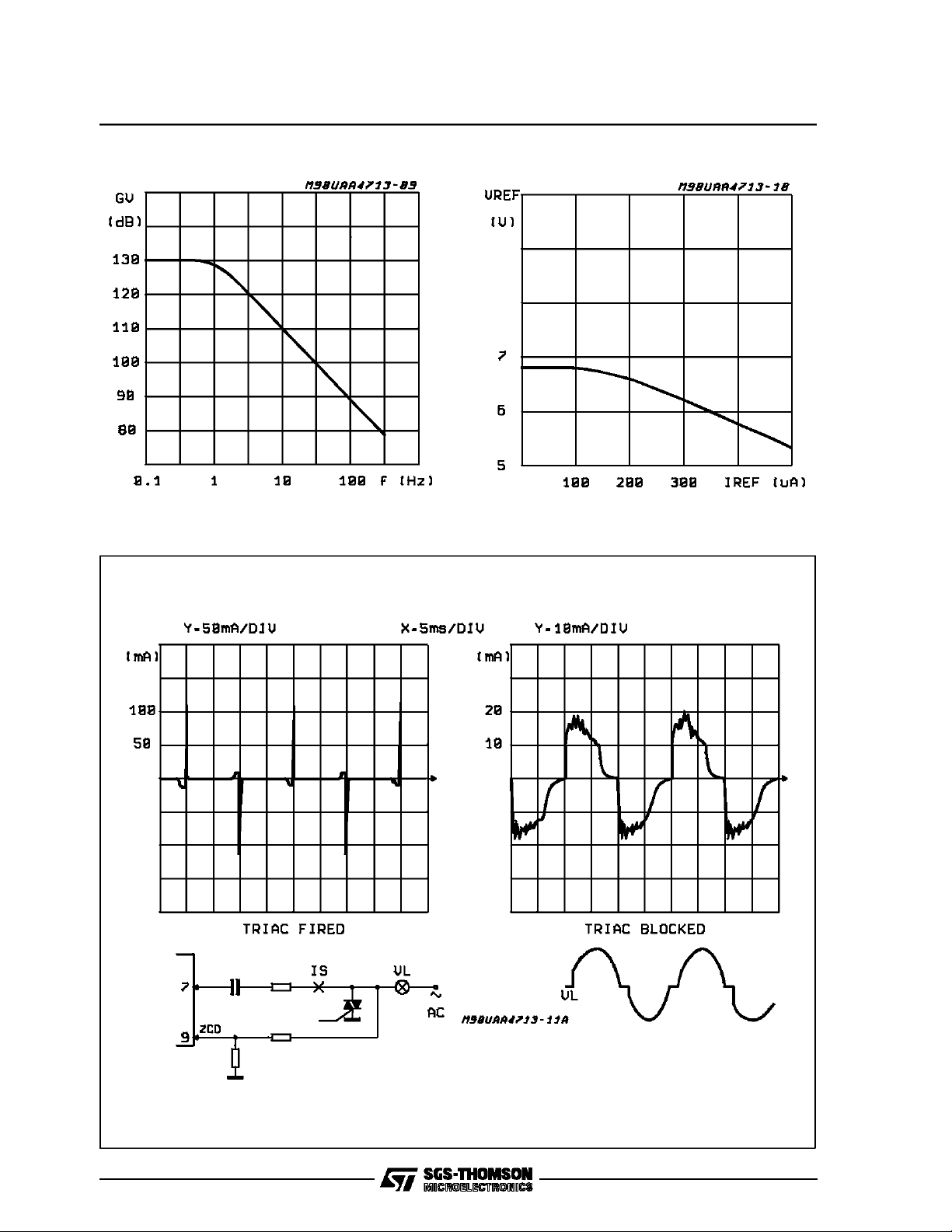
Figure1: Open Loop FrequencyResponse
Figure3: SupplyCurrent
Figure2: V
REF
versusI
REF
5/14
 Loading...