

SGS Thomson Microelectronics UA776CN Datasheet

.
MICROPOWEROPERATION
.
NO FREQUENCY COMPENSATION
REQUIRED
.
WIDEPROGRAMMINGRANGE
.
HIGHSLEWRATE
.
SHORT-CIRCUIT PROTECTION
.
PROGRAMMABLESINGLE OP-AMP
UA776
PROGRAMMABLE LOW POWER
SINGLE OPERATIONALAMPLIFIERS
DESCRIPTION
The UA776programmableoperationalamplifier is
characterized by low supply current and low
equivalentinput noisevoltageoverawiderangeof
operating supply voltages.
Coupled with programmable electrical characteristics, it is a versatile amplifier for use in high
accuracy,low power consumptionanalog applications.
Input noise voltage and current, power consumption and input current can be optimizedby a single
resistor or current source that sets the chip quiescent current for nano-watt power consumptionor
for characteristicssimilar to the UA741.
Internalfrequencycompensation,absenceof latch
up, high slew rate and short-circuitprotection assure ease of use in long time integrators, active
filters, and sample and hold circuits.
N
DIP8
(Plastic Package)
ORDER CODES
Part
Number
UA776C 0
UA776I -40
UA776M -55
Example : UA776CN
PIN CONNECTIONS (top view)
1
2
3
4
1 - Offset null 1
2 - Inverting input
3 - Non-inverting input
-
4-V
CC
5 - Offset null 2
Temperature
Range
o
C, +70oC ••
o
C, +105oC ••
o
C, +125oC ••
(Plastic Micropackage)
6 - Output
7-V
8-I
set
D
SO8
Package
ND
+
CC
8
7
6
5
December 1997
1/8
UA776
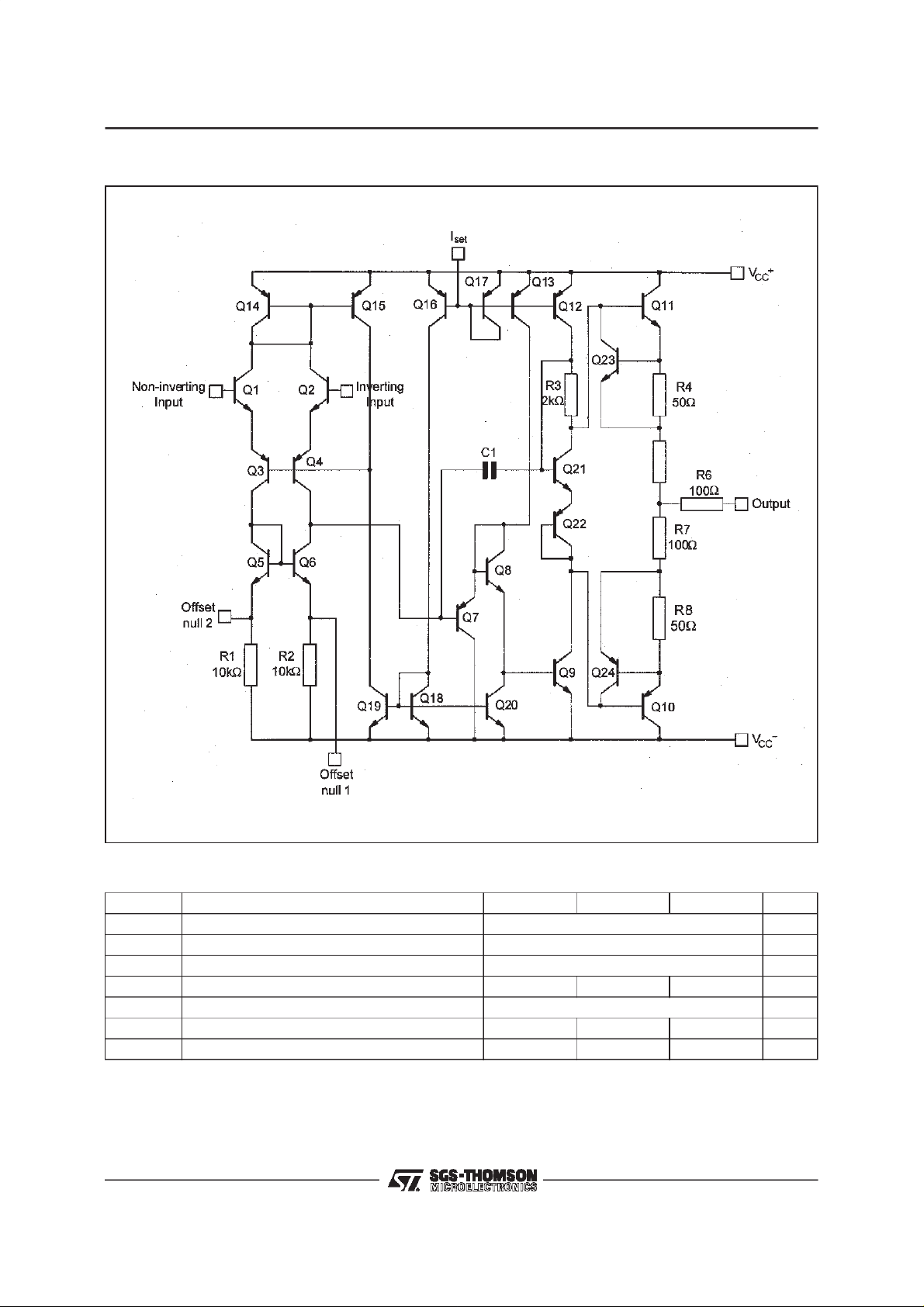
SCHEMATICDIAGRAM
ABSOLUTEMAXIMUMRATINGS
Symbol Parameter UA776M UA776I UA776C Unit
V
V
V
P
T
oper
T
stg
Note : 1. For supply voltages less than±15V, the absolute maximum input voltage is equal to the supply voltage.
2/8
Supply Voltage ±18 V
cc
Differential Input Voltage ±30 V
id
Input Voltage - (note 1) ±15 V
i
Power Dissipation 500 310 310 mW
tot
Output Short-circuit Duration Infinite
Operating Free Air Temperature Range -55 to +125 -40 to +105 0 to +70
Storage Temperature Range -65 to +150 -65 to +150 -65 to +150
o
C
o
C
UA776
ELECTRICALCHARACTERISTICS VCC
Symbol Parameter
V
A
SVR Supply Voltage Rejection Ratio(R
I
V
CMR Common-mode Rejection Ratio (R
Input Offset Voltage
I
I
CC
icm
io
io
ib
vd
= +25oC
T
amb
≤ T
T
min.
amb
≤ T
max.
Input Offset Current
= +25oC
T
amb
≤ T
T
min.
amb
≤ T
max.
Input Bias Current
= +25oC UA776M
T
amb
UA776I,C
≤ T
T
min.
amb
≤ T
max.
Large Signal Voltage Gain (VO±10V)
= +25oCR
T
amb
= 75kΩ
R
L
≤ T
T
min.
R
L
T
amb
T
min.
amb
=5kΩ
= +25oC
≤ T
amb
≤ T
≤ T
max.
max.
Supply Current, no load
= +25oC
T
amb
≤ T
T
min.
amb
≤ T
max.
Input Common Mode Voltage Range ±10 ±10 V
= +25oC
T
amb
≤ T
T
min.
amb
≤ T
max.
±15V,T
=5kΩ
L
RL= 75kΩ
≤ 10kΩ)
S
≤ 10kΩ)
S
= +25oC (unless otherwise specified)
amb
I
= 1.5µAI
set
set
Min. Typ. Max. Min. Typ. Max.
25
6
0.7 3
10
2
7.5
2
10
20
10075400
200
400
100
777792 777792
20 25
30
707090 707090
=15µA
25
6
215
40
151550
50
100
160 180
200
Unit
mV
nA
nA
V/mV
dB
µA
dB
I
±V
V
SR Slew Rate (V
K
R
C
R
GBP Gain Bandwidth Product (C
Output Short-circuit Current 0.5 3 15 6 12 30 mA
OS
Output Voltage Swing
OPP
ior
t
r
OV
I
id
o
= +25oCR
T
amb
= 75kΩ
R
L
≤ T
T
min.
amb
≤ T
max.
Offset Voltage Adjustment Range 9 18 mV
= ±10V, CL= 100pF, unity gain)
i
=5kΩ
R
L
= 75kΩ
R
L
Rise Time (Vi= ±20mV, CL= 100pF, unity gain)
=5kΩ
R
L
= 75kΩ
R
L
Overshoot (Vi= ±20mV, CL = 100pF, unity gain)
=5kΩ
R
L
= 75kΩ
R
L
Input Resistance 50 5 MΩ
Differential Input Capacitance 2 2 pF
Output Resistance 5 1 kΩ
= 100pF,T
f = 100kHz R
L
f = 10kHz R
THD Total Harmonic Distortion (f = 1kHz, A
=2VPP,CL= 100pF, T
V
O
=5kΩ
R
L
= 75kΩ
R
L
amb
=25oC)
en Equivalent Input Noise Voltage
(f = 1kHz, R
= 100Ω)4020
s
=5kΩ
L
RL= 75kΩ 121014
0.01 0.1
1.6
=25oC)
amb
=5kΩ
L
= 75kΩ
L
V
= 20dB,
0.3 0.1
0.8
V
101013
V/ms
0.2 0.8
ms
0.35
%
10
0
MHz
0.4 0.7
%
0.025
nV
√Hz
3/8
 Loading...