

TSTM872-20
RF POWER MODULE
MOBILE APPLICATIONS
PRODUCTDEVELOPMENTDATA SHEET
This datasheetcontainsthe designcriteriaand target specificationsfor a product whichis currentlyunder
development by SGS-THOMSON. The design criteria and specificationsof this item could change prior
to introductionand SGS-THOMSONassumes no liabilityfor use of information contained herein.
.MOBILE CLASS C POWER AMPLIFIER
.806 - 870 MHz
.12.5 VOLTS
.INPUT/OUTPUT 50 OHMS
.P
OUT
20 W MIN.
=
.GAIN = 19 dB MIN.
ORDERCODE
TSTM872-20
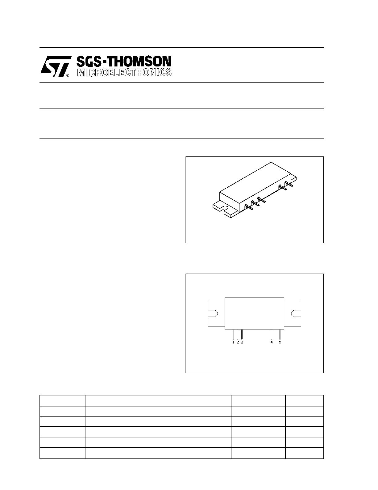
PIN CONNECTI ON
DESCRIP TIO N
The TSTM872-20 module is designed f or high
power, h igh efficiency, analog private mobile
radio syste ms in the 80 6 - 870 MHz freque ncy
range.
A s ignificant advantage of this module is its
high RF power output p erformance a nd very
low stan dby current.
ABSOLUTE MAXIMUM RATINGS (Tcase=25°C)
Symbol Parameter Value Unit
VS1,VS2,VS3DC Sup ply Voltag e 16 Vdc
RF In put Pow er 400 mW
RF Ou tput Powe r 25 W
Storage Temperature
Operating Case Temperature
P
T
P
OUT
STG
T
IN
C
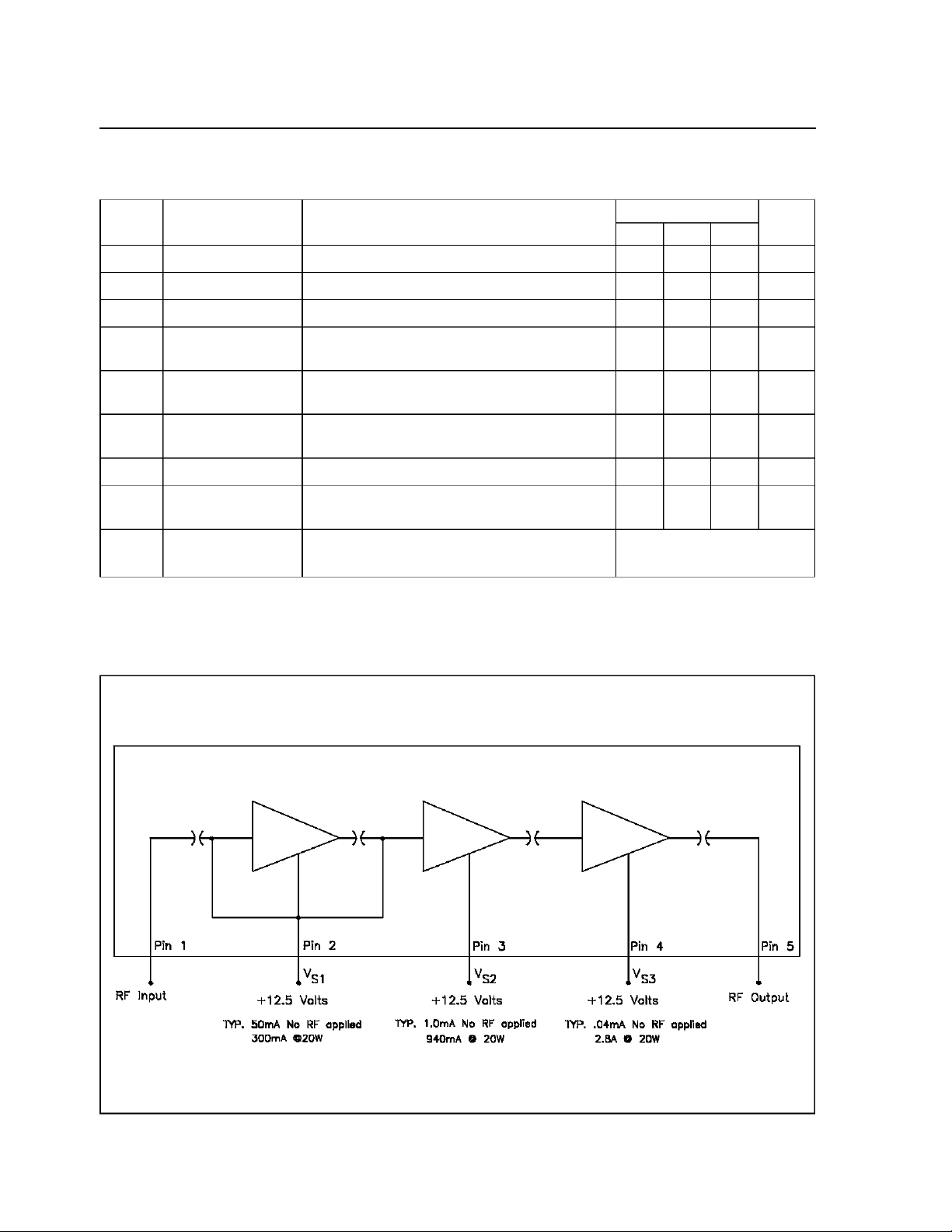
1. RF Input 2. 12.5 Vdc VS13. 12.5 Vdc V
4. 12.5 Vdc V
S3
5. RF Output
− 30 to +100
− 30 to +100
BRANDING
TSTM872-20
S2
°
C
°
C
TSTM8 72-20
ELECTRICAL S PEC I FICATIONS (T
Symbol Parame ter Test Co ndition s
case
unless otherwise noted.)
25°C, V
=
S1,VS2,VS3
12.5 Volts
=
Min. Typ. Max.
Value
BW Frequency Range 806 — 870 MHz
P
I
Q1(q)
I
Q2(q)
I
Q3 (q)
Z
Input Power
IN
η
Efficiency
Quiescent Current
V
S1
Quiescent Current
V
S2
Quiescent Current
V
S3
H Harmonics
Input Impedance
IN
— Load Mismatch
P
P
OUT
OUT
= 20 W
20 W
=
— — 250 mW
35 40 — %
No RF applied — 50 — mA
No RF applied — 1.0 — mA
No RF applied — 0.04 — mA
P
P
OUT
OUT
20 W
=
= 20 W
VSWR=30:1 V=16 Vdc
OUT
=
25 W
P
—
−58
— — 2.0:1 VSWR
No Degradation in
Output Power
—dBc
Uni t
INTERNAL CO NFIGURATIO N

APPLICATIONS RECOMME NDATI ONS
TSTM8 72-20
OPERATION LIMITS
The TSTM872-20 power module should never be
operated under any condition which exceeds the
Absolute Maximum Ratings presented on this
data sheet. Nor should the module be operated
continuously at any of the specified maximum ratings. If the module is to be subjected to one or
more of the maximum rating conditions, care
must be taken to monitor other parameters which
may be affected.
DECOUPLING
Failure to properly decouple any of the voltage
supply pins will result in oscillations at certain operating frequencies. Therefore, it is recommended
that these pins be bypassed as indicated in the
Module DC and Test Fixture Configuration drawing of this data sheet.
MODULE MOUN TING
To insure adequate thermal transfer from the
module to the heatsink, it is recommended that a
satisfactory thermal compound such as Dow
Corning 340, Wakefield 120-2 or equivalent be
applied between the module flange and the
heatsink.
The heatsink mounting surface under the module
should be flat to within +/- 0.05 mm (+/- 0.002
inch). The module should be mounted to the
heatsink using 3.5 mm (or 6-32) or equivalent
screwstorques to 5-6 kg-cm (4-6 in-lb).
The module leads should be attached to equipment PC board using 180°C solder applied to the
leads with a properly grounded soldering iron tip,
not to exceed 195°C, applied a minimum of 2 mm
(0.080”) from the body of the module for a duration not to exceed 15 seconds per lead. It is imperative that no other portion of the module, other
than the leads, be subjected to temperatures in
excess of 100°C (maximum storage temperature),
for any period of time, as the plastic moulded
cover, internal components and sealing adhesives
may be adversely affected by such conditions.
Due to the construction techniques and materials
used within the module, reflow soldering of the
flange heatsink or leads, is not recommended.

PACKAGE MECHANICAL DAT A
Ref.: Dwg. No. M12-030 rev. C
TSTM8 72-20
Infor mat ion fur ni shed is bel ieved t o be accurat e and reliable. However, S GS-THO MSON Microelectronics assumes no responsibi lity for the consequences of use of such inf or mat ion nor for any infr ingement of pa t ents or ot her right s of thi r d parties wh ich
may r esul t from it s use. N o li cense is granted by i m pl ication or oth erw i se under any patent or patent rights of SGS-T H OMS O N
Micr oel ectronics. Specifications mentioned i n t his publi cation are subjec t to change without n ot ice. T hi s publication super sedes
and replaces all information previously supplied. SGS-THOMSON Microelectronics products are not authorized for use as critical
components in li f e s upport devices or systems w i t hout express writ t en approval of SGS -T H OMS O N Microele ctr oni cs.
1995 SGS-THOMSON Microelectronics - All Rights Reserved
Austr alia - Brazil - France - German y - Hong Kong - It aly - Jap an - Korea - Malaysia - Malta - Morocco - The N et her l ands -
Singapor e - Spai n - Sweden - Sw it zerland - Taiwan - Thailand - Unit ed K i ngdom - U.S .A.
SGS-THOMSON Microelectronics GROUP OF COMPANIES
 Loading...