

SGS Thomson Microelectronics TSM109IN, TSM109ID, TSM109IDT, TSM109AIN, TSM109AIDT Datasheet
...
1/7
COMPARATOR
■ LOW SUPPLY CURRENT (1.1mA) INDE-
PENDENT OF SUPPLY VOLTAGE
■ LOW INPUT BIAS CURRENT : 25nA TYP
■ LOW INPUT OFFSET VOLTAGE : ±1mV TYP
■ INPUT COMMON-MODE VOLTAGE RANGE
INCLUDES GROUND
■ LOW OUTPUT SATURATION VOLTAGE :
250mV TYP; (Io = 4mA)
■ DIFFERENTIAL INP U T VOLTAGE RA NGE
EQUAL TO THE SUPPLY VOLTAGE
■ WIDE POWER SUPPLY RANGE : ±1V to
±18V
■ ESD PROTECTION : 1.5kV
VOLTAGE REFERENCE
■ Fixed V
ref
to 2.5V
■ 0.4% AND 1% VOLTAGE PRECISION
■ SINK CURRENT CAPABILITY : 1 to 100mA
DESCRIPTION
The TSM109 i s a monoli thic IC that i ncludes two
comparators and a shunt vol tage reference. Thi s
device offers space and cos t s avings i n m any ap plications including p ower supply management o r
data acquisition systems.
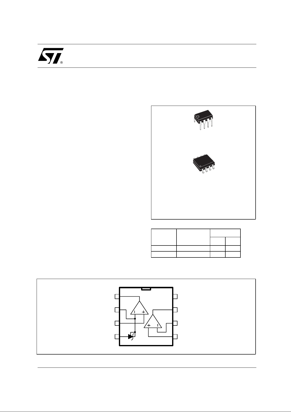
ORDER CODE
N = Dual in Line Package (DIP)
D = Small Outline Package (SO) - also available in Tape & Reel (DT)
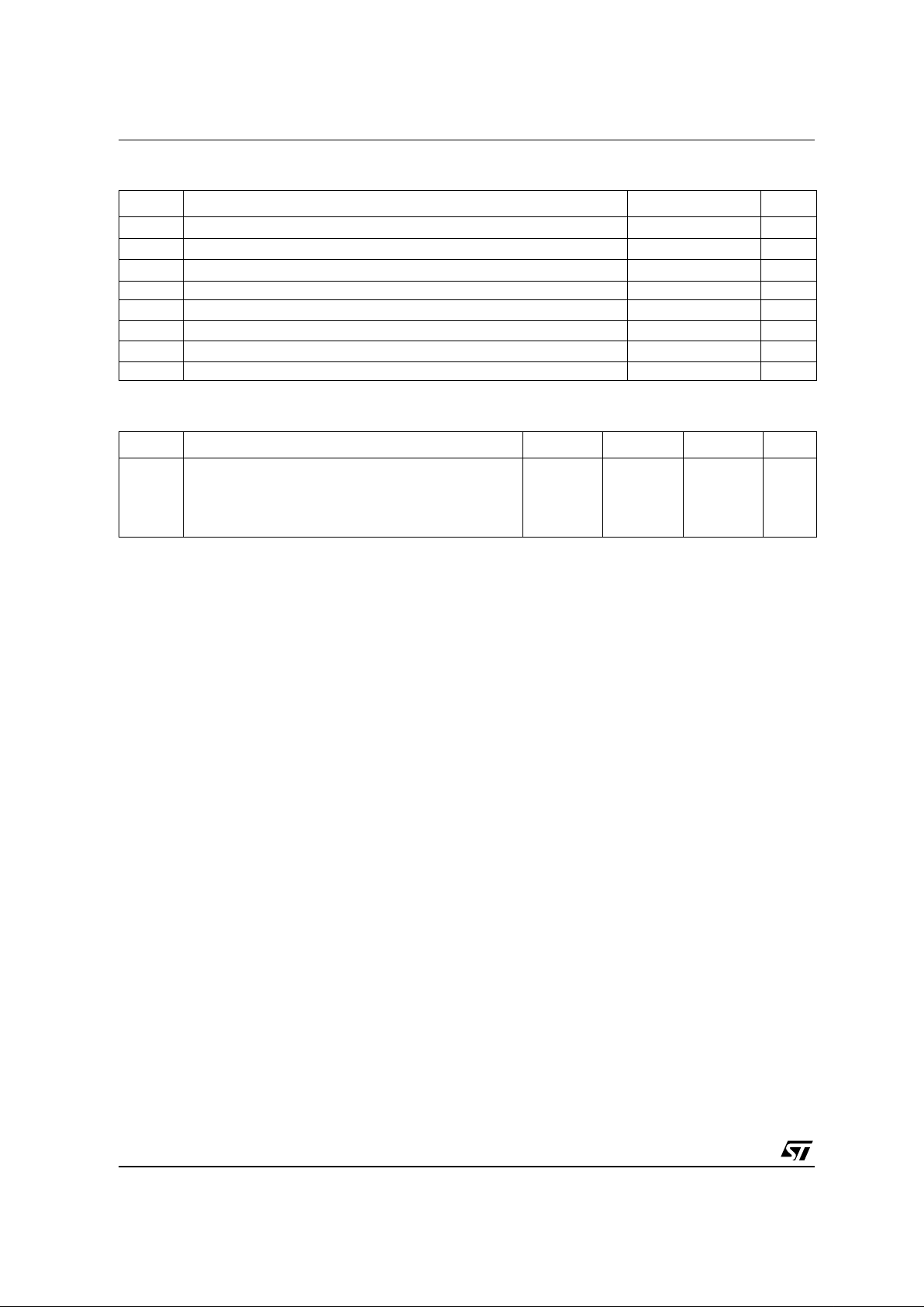
PIN CONNECTIONS (top view)
Part
Number
Temperature
Range
Package
ND
TSM109 -40°C, +105°C
••
TSM109A -40°C, +105°C
••
D
SO8
N
DIP8
1
2
3
4
5
6
7
8
Gnd
Ve+
Ve+
Ve-
Out
Vcc
Vref
Out
TSM109/A
DUAL COMPARATOR AND VOLTAGE REFERENCE
November 2002
TSM109/A
2/7
ABSOLUTE MAXIMUM RATINGS
ELECTRICAL CHARACTERISTICS
V
CC
+
= 5V, V
CC
-
= 0V, T
amb
= 25°C (unless otherwise specified)
Symbol Parameter Value Unit
V
CC
Supply voltage 36 V
V
id
Differential Input Voltage 36 V
V
in
Input Voltage
-0.3 to V
cc
+0.3
V
Ik Continuous Cathode current range -100 to 150 mA
T
oper
Operating Free-air Temperature Range -40 to105 °C
T
j
Maximum Junction Temperature 150 °C
R
thja
Thermal Resistance Junction to Ambient (SO package) 175 °C/W
ESD Electrostatic Discharge Protection 1.5 kV
Symbol Parameter Min Typ Max Unit
I
CC
Total Supply Current, excluding current in the Voltage
Reference
V
CC
= +5V, no load
V
CC
= +30V, no load
0.4
1
1
2.5
mA
TSM109/A
3/7
ELECTRICAL CHARACTERISTICS
COMPARATOR (independent comparator)
V
CC
+
= +5V, V
CC
-
= GND, T
amb
= +25°C (unless otherwise specified)
Symbol Parameter
TSM109
Unit
Min. Typ. Max.
V
io
Input Offset Voltage - note 1)
T
amb
= +25°C
T
min
≤ T
amb
≤ T
max
1. At output switch point, Vo ≈ 1.4V, Rs = 0 with V
CC
+
from 5V to 30V, and over the full common-mode range (0V to V
CC
+
-1.5V).
15
9
mV
I
io
Input Offset Current
T
amb
= +25°C
T
min
≤ T
amb
≤ T
max
325
100
nA
I
ib
Input Bias Current (I+ or I-) - note
2)
T
amb
= +25°C
T
min
≤ T
amb
≤ T
max
2. The direction of the input current is out of the IC due to the PNP input stage. This current is essentially constant, independent of the state of the
output, so no loading charge exists on the reference of input lines.
25 250
400
nA
A
vd
Large Signal Voltage Gain
V
CC
= 15V, RL = 15k
Ω,
Vo = 1V to 11V
50 200 V/mV
V
icm
Input Common Mode Voltage Range - note
3)
V
CC
= 30V
T
amb
= +25°C
T
min
≤ T
amb
≤ T
max
3. The input common-mode voltage of either input signal voltage should not be allowed to go negative by more than 0.3V. The upper end of the
common-mode voltage range is V
CC
+
-1.5V, but either or both inputs can go to +30V without damage.
0
0
V
CC
+
-1.5
V
CC
+
-2
V
V
id
Differential Input Voltage -note
4)
4. Positive voltage excursions of one input may exceed the power supply level. As long as the other input voltage remains within the common-mode
range, the comparator will provide an appropriate output state. The low input voltage state must not be less than -0.3V (or 0.3V below the negative
power supply, if used).
V
CC
+
V
OL
Low Level Output Voltage
V
id
= -1V, I
sink
= 4mA
T
amb
= +25°C
T
min
≤ T
amb
≤ T
max
250 400
700
mV
I
OH
High Level Output Current (Vid = 1V)
V
CC
= Vo = 30V
T
amb
= +25°C
T
min
≤ T
amb
≤ T
max
30 150
1
nA
µ
A
I
sink
Output Sink Currrent
V
id
= 1V, Vo = 1.5V
10 20 mA
t
re
Response Time - note 5)
R
L
= 5.1kΩ connected to V
CC
+
5. The response time specified is for a 100mV input step with 5mV overdrive. For larger overdrive signals, 300ns can be obtained
1.3
µ
s
t
rel
Large Signal Response Time
R
L
= 5.1kΩ connected to V
CC
+
, el = TTL,
V
(ref)
= +1.4v
300 ns

TSM109/A
4/7
COMPARATOR (comparator with inverting input connected to the internal Vref))
V
CC
+
= +5V, V
CC
-
= GND, T
amb
= +25°C (unless otherwise specified)
Symbol Parameter
TSM109
Unit
Min. Typ. Max.
V
io
Input Offset Voltage - note 1)
T
amb
= +25°C
T
min
≤ T
amb
≤ T
max
1. At output switch point, Vo ≈ 1.4V, Rs = 0 with V
CC
+
from 5V to 30V, and over the full common-mode range (0V to V
CC
+
-1.5V).
15
9
mV
I
ib
Input Bias Current for positive input note
2)
T
amb
= +25°C
T
min
≤ T
amb
≤ T
max
2. The direction of the input current is out of the IC due to the PNP input stage. This current is essentially constant, independent of the state of the
output, so no loading charge exists on the reference of input lines.
25 250
400
nA
A
vd
Large Signal Voltage Gain
V
CC
= 15V, RL = 15k
Ω,
Vo = 1V to 11V
50 200 V/mV
V
OL
Low Level Output Voltage
V
id
= -1V, I
sink
= 4mA
T
amb
= +25°C
T
min
≤ T
amb
≤ T
max
250 400
700
mV
I
OH
High Level Output Current (Vid = 1V)
V
CC
= Vo = 30V
T
amb
= +25°C
T
min
≤ T
amb
≤ T
max
30 150
1
nA
µ
A
I
sink
Output Sink Currrent
V
id
= 1V, Vo = 1.5V
10 20 mA
t
re
Response Time - note 3)
R
L
= 5.1kΩ connected to V
CC
+
3. The response time specified is for a 100mV input step with 5mV overdrive. For larger overdrive signals, 300ns can be obtained.
1.3
µ
s
t
rel
Large Signal Response Time
R
L
= 5.1kΩ connected to V
CC
+
, el = TTL,
V
(ref)
= +1.4v
300 ns

TSM109/A
5/7
ELECTRICAL CHARACTERISTICS
VOLTAGE REFERENCE
T
amb
= 25°C (unless otherwise specified)
Symbol Conditions Value Unit
I
K
Cathode Current 1 to 100 mA
Symbol Parameter
TSM109A TSM109
Unit
Min. Typ. Max. Min. Typ. Max.
V
ref
Reference Input Voltage, IK = 10 mA
T
amb
= 25°C
T
min
≤ T
amb
≤ T
max
2.490
2.48
2.500 2.510
2.52
2.475
2.45
2.500 2.525
2.55
V
∆
V
ref
Reference Input Voltage Deviation OverT emperature
Range I
K
= 10 mA
T
min
≤T
amb
≤ T
max
7 30 7 30 mV
Temperature Coefficient of Reference Input Voltage
I
K
= 10 mA,
T
min
≤T
amb
≤ T
max
±13 ±90 ±13 ±90 ppm/°C
I
min
Minimum Cathode Current for Regulation 0.5 1 0.5 1
mA
|Z
Vref
|
Dynamic Impedance - note
1)
∆
V
ref
, ∆IK = 1 to 100mA, f < 1KHz
1. The dynami c im pedance is de fined as [Z
Vref
| = ∆V
Vref
/∆I
K
0.3 0.65 0.3 0.65
Ω
∆
Vref
Vref∆T
--------------------
TSM109/A
6/7
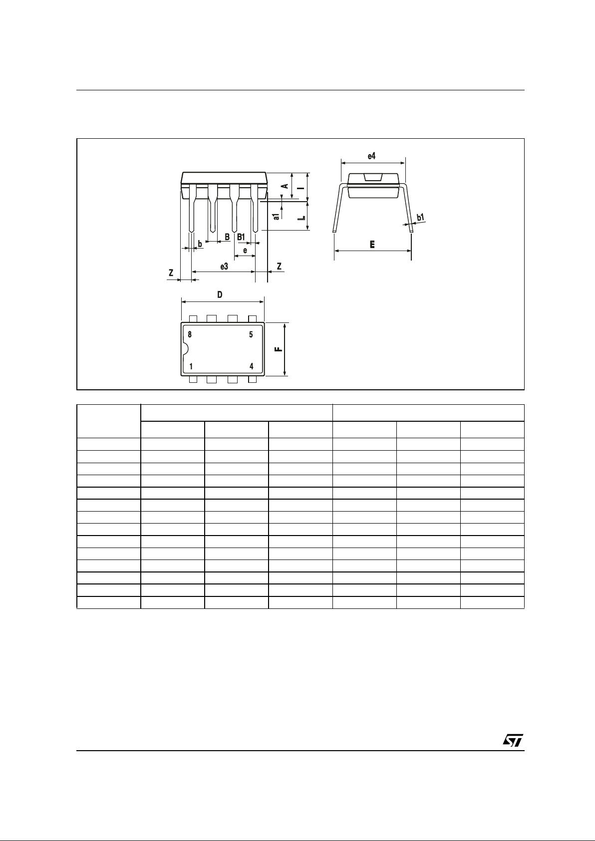
PACKAGE MECHANICAL DATA
8 PINS - PLASTIC DIP
Dimensions
Millimeters Inches
Min. Typ. Max. Min. Typ. Max.
A 3.32 0.131
a1 0.51 0.020
B 1.15 1.65 0.045 0.065
b 0.356 0.55 0.014 0.022
b1 0.204 0.304 0.008 0.012
D 10.92 0.430
E 7.95 9.75 0.313 0.384
e 2.54 0.100
e3 7.62 0.300
e4 7.62 0.300
F 6.6 0260
i 5.08 0.200
L 3.18 3.81 0.125 0.150
Z 1.52 0.060

TSM109/A
7/7
PACKAGE MECHANICAL DATA
8 PINS - PLASTIC MICROPACKAGE (SO)
Dimensions Millimeters Inches
Min. Typ. Max. Min. Typ. Max.
A 1.100 0.043
A1 0.050 0.100 0.150 0.002 0.004 0.006
A2 0.780 0.860 0.940 0.031 0.034 0.037
b 0.250 0.330 0.400 0.010 0.013 0.016
c 0.130 0.180 0.230 0.005 0.007 0.009
D 2.900 3.000 3.100 0.114 0.118 0.122
E 4.750 4.900 5.050 0.187 0.193 0.199
E1 2.900 3.000 3.100 0.114 0.118 0.122
e 0.650 0.026
L 0.400 0.550 0.700 0.016 0.022 0.028
L1 0.950 0.037
k 0d3d6d0d3d6d
aaa 0.100 0.004
Information furnished is belie ved to be accurate and reliable. However, STMicroelec tronics assumes no responsibility for the
consequences of use of such information nor for any infringement of patents or other rights of third parties which may result from
its use. No license is granted by implication or otherwise under any patent or patent rights of STMicroelectronics. Specifications
mentioned in this publication are subject to change without notice. Thi s publication supersedes and replaces all information
previously supplied. STMicroelectroni cs products are not author ized for use as critical c omponents in life support de vices or
systems without express written approval of STMicroelectronics.
The ST logo is a registered trademark of STMicroelectronics
© 2002 STM i cr o electroni cs - All Rights Reserved
STMicroele ctronics GROUP OF COMP ANIES
Australi a - B razil - China - Finland - Fran ce - Germany - Hon g Kong - India - Ita l y - J apan - Malaysi a - M al ta - Morocco
Singapore - Spain - Sweden - Switzerland - United Kingdom
http://www.st.com
 Loading...