

1/9
■ CONSTANT VOLTAGE AND CONSTANT
CURRENT CONTROL
■ LOW VOLTAGE OPERATION
■ PRECISION INTERNAL VOLTAGE REFER-
ENCE
■ LOW EXTERNAL COMPONENT COUNT
■ CURRENT SINK OUTPUT STAGE
■ EASY COMPENSATION
■ LOW AC MAINS VOLTAGE REJECTION
DESCRIPTION
TSM105 is a hi ghly integrated solut ion for SMPS
applications requiring CV (cons tant voltage) and
CC (constant current) mode.
TSM105 integrates one voltage reference, two
operational amplifiers (with OR ed outputs - common collectors), and a current sensing circuit.
The voltage reference combined with one operational amplifier mak es it an ideal voltage cont roller, and the other low voltage reference combined
with the other operational amplifier makes it an
ideal current limiter for output low side current
sensing.
The current threshold is fixed, and precise.
The only external components are:
* a resistor bridge to be connected on the output of
the power supply (adapter, battery charg er) to set
the voltage regulation by dividing the desired output voltage to match the internal v oltage reference
value.
* a sense resistor whos e valu e and allowable dissipation power need to be chosen according to the
internal voltage threshold.
* optional compensation components (R and C).
TSM105, housed in o ne of the smallest package
available, is ideal for space shri nked applications
such as adapters and battery chargers.
APPLICATIONS
■ ADAPTERS
■ BAT TERY CHARGERS
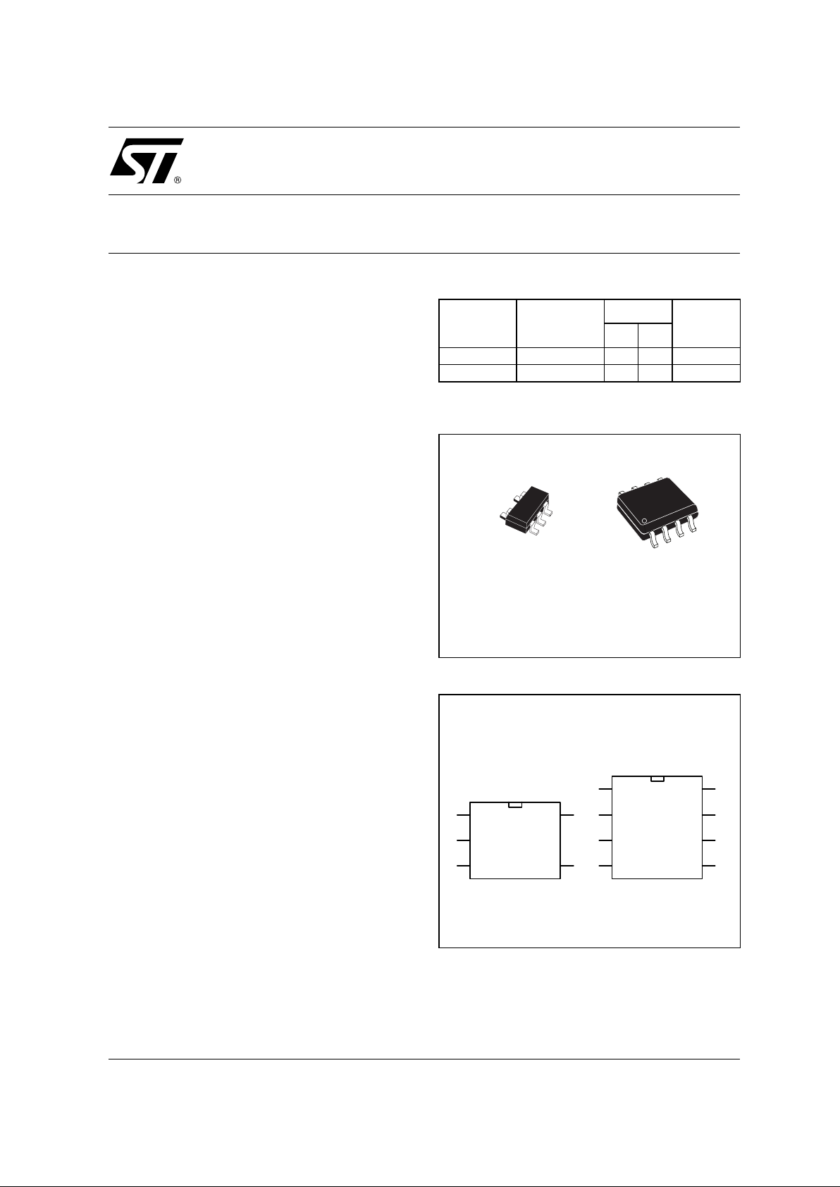
ORDER CODE
L = Tiny Package (SOT23-5) - only available in Tape & Reel (LT)
D = Small Outline Package (SO) - also available in Tape & Reel (DT)
PIN CONNECTIONS (top view)
Part
Number
Temperature
Range
Package
Marking
LD
TSM105CLT 0 to 85°C • M105
TSM105CD 0 to 85°C • TSM105
L
SOT23-5
(Plastic Package)
D
SO8
(Plastic Micropackage)
1
2
34
5Vctrl
Gnd
Vcc
IctrlOut
1
2
3
45
6
Vctrl Gnd
Vcc
Nc
Out
Ictrl
Nc
Nc
SOT23-5
SO8
7
8
September 2001
TSM105
CONSTANT VOLTAGE AND CONSTANT CURRENT
CONTROLLER FOR BATTERY CHARGERS AND ADAPTORS
TSM105
2/9
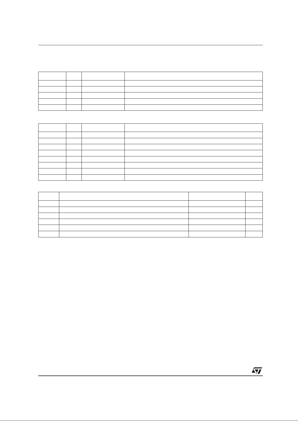
PIN DESCRIPTION
SOT23-5 Pinout
SO8 Pinout
ABSOLUTE MAXIMUM RATINGS
Name Pin # Type Function
Vcc 5 Power Supply Positive Power Supply Line
Gnd 2 Power Supply Ground Line. 0V Reference For All Voltages
Vctrl 1 Analog Input Input Pin of the Voltage Control Loop
Ictrl 4 Analog Input Input Pin of the Current Control Loop
Out 3 Current Sink Output Output Pin. Sinking Current Only
Name Pin # Type Function
Vcc 2 Power Supply Positive Power Supply Line
Gnd 8 Power Supply Ground Line. 0V Reference For All Voltages
Vctrl 1 Analog Input Input Pin of the Voltage Control Loop
Ictrl 6 Analog Input Input Pin of the Current Control Loop
Out 7 Current Sink Output Output Pin. Sinking Current Only
NC 3
NC 4
NC 5
Symbol DC Supply Voltage Value Unit
Vcc DC Supply Voltage 14 V
Vi Input Voltage -0.3 to Vcc V
Top Operating Free Air Temperature Range -55 to 125 °C
Tj Maximum Junction Temperature 150 °C
Rthja Thermal Resistance Junction to Ambient SO8 package 130 °C/W
Rthja Thermal Resistance Junction to Ambient SOT23-5 package 250 °C/W
TSM105
3/9
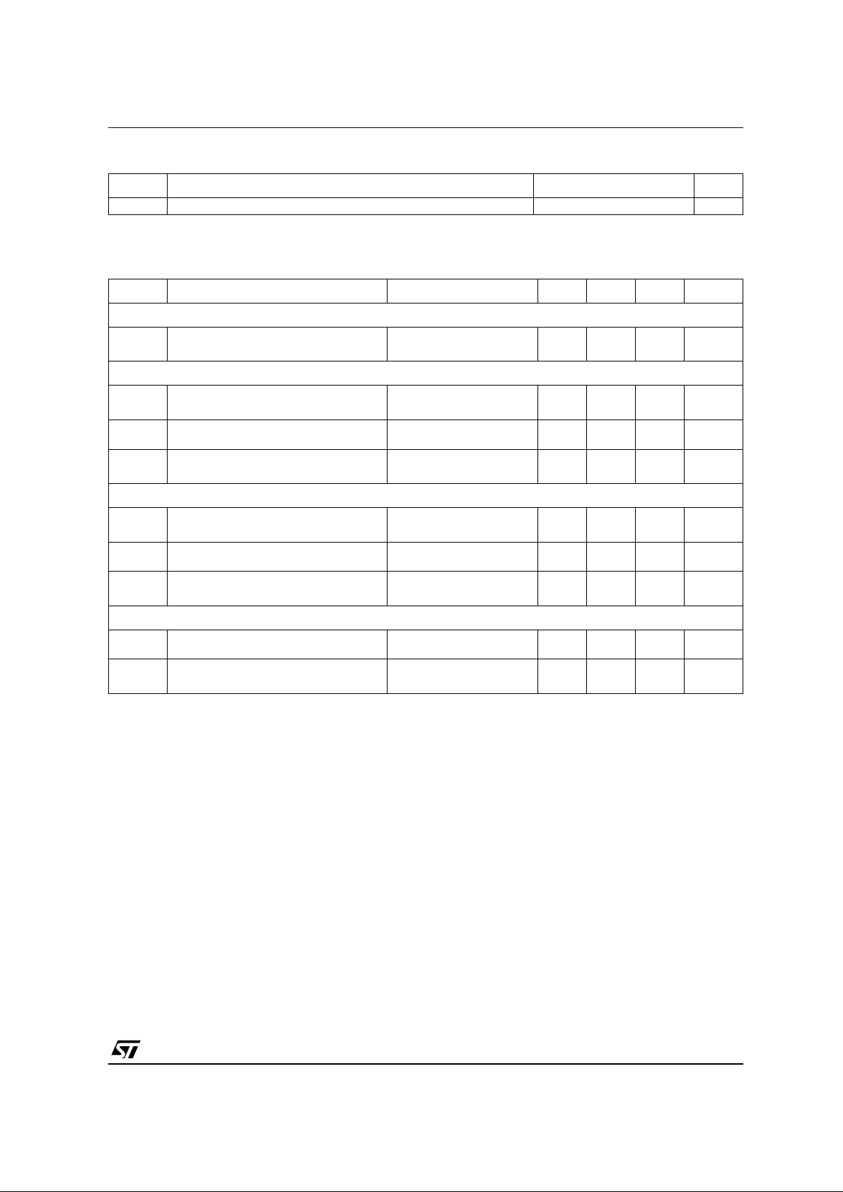
OPERATING CONDITIONS
ELECTRICAL CHARACTERISTICS
Tamb = 25°C and Vcc = +5V (unless otherwise specified)
Symbol Parameter Value Unit
Vcc DC Supply Conditions 2.8 to 12 V
Symbol Parameter Test Condition Min Typ Max Unit
Total Current Consumption
Icc Total Supply Current - not taking the
output sinking current into account
Tamb
0 < Tamb < 85°C
1.05
1.2
2mA
Voltage Control Loop
Gmv Transconduction Gain (Vctrl). Sink
Current Only
1)
1. If the vol tage on VCTRL (the negative input of th e amplifier) is high er than the positive am pl i fier input (Vref=1. 210V), and it is increased
by 1mV, the sinking current at the output OUT will be increased by 3.5mA.
Tamb
0 < Tamb < 85°C
1 3.5
2.5
mA/mV
Vref
Voltage Control Loop Reference
2)
2. The internal Voltage Reference is set at 1.210V (bandgap reference). The voltage control loop precision takes into account the cumulative
effects of the internal voltage reference deviation as we l l as the i nput offs et volta ge of the trans-conductance operati onal amplifier . The
internal V ol t age Referen ce is fixed by bandgap, and trimm ed to 0.5% accuracy at room temperaure.
Tamb
0 < Tamb < 85°C
1.198
1.186
1.21 1.222
1.234
V
Iibv Input Bias Current (Vctrl) Tamb
0 < Tamb < 85°C
50
100
nA
Current Control Loop
Gmi Transconduction Gain (Ictrl). Sink
Current Only
3)
3. When the positive input at ICTRL is lower than -20 0mV, and the vol t age is decreased by 1mV, t he sinking cur rent at the out put OUT will
be increased by 7mA.
T amb
0 < Tamb < 85°C
1.5 7
4
mA/mV
Vsense
Current Control Loop Reference
4)
4. The internal current sense threshold is set to -200mV. The current control loop precision takes into account the cumulative effects of the
internal vo l tage reference deviation as well as the in put offset volta ge of the trans -c onductance operational am plifier.
Iout = 2.5mA Tamb
0 < Tamb < 85°C
196
192
200 204
208
mV
Iibi Current out of pin ICTRL at -200mV Tamb
0 < Tamb < 85°C
25
50
µA
Output Stage
Vol Low output voltage at 10 mA sinking
current
Tamb 200 mV
Ios Output Short Circuit Current. Output to
Vcc. Sink Current Only
Tamb
0 < Tamb < 85°C
27
35
50 mA

TSM105
4/9
In the above application schem atic, the TSM105 i s used on the secon dary side of a flyback ad apter (or
battery charger) to provide an accurate control of voltage and current. The above feedback loop is made
with an optocoupler.
Figure 1 : Internal Schematic
Figure 2 : Typical Adapter or Battery Charger Application Using TSM105
+
-
+
-
1.210V
200mV
Vcc
Out
Vctrl
Gnd
Ictrl
+
-
+
-
1.210V
200mV
Vcc
Out
Vctrl
Gnd
Ictrl
D
+
R2
R1
Rsense
Rvc1
470K
Cvc1
2.2nF
Ric1
22
To primary
OUT+
OUT-
+
TSM105
Cic1
100nF
Cvc2
22pF
Load
IL
IL
Vsense

5/9
1. Voltage and Cu rren t Co ntro l
1.1. Voltage Control
The voltage loop is controlled via a first transconductance operational am plifier, the resist or brid ge
R1, R2, and the optocoupler which is directly connected to the output.
The relation between the values of R1 and R2
should be chosen as writen in Equation 1.
R1 = R2 x Vref / (Vout - Vref) Eq1
where Vout is the desired output voltage.
To avoid the discharge of the load, the resistor
bridge R1, R2 should be highly resist ive. For this
type of application, a total value of 100KΩ (or
more) would be appropriate for the resistors R1
and R2.
As an example, wi th R2 = 100K Ω, Vout = 4.10V,
Vref = 1.210V, then R1 = 41.9KΩ.
Note that if the low drop diode should be inserted
between the load and the voltage regulation resistor bridge to avoid current flowing from the load
through the resistor bridge, this drop should be
taken into account in the above calculations by replacing Vout by (Vout + Vdrop).
1.2. Current Control
The current loop is controlled via the second
trans-conductance operational amplifier, the
sense resistor Rsense, and the optocoupler.
The control equation verifies:
Rsense x Ilim = Vsense e q2
Rsense = Vsense / Ilim eq2’
where Ilim is the desired limited current, and
Vsense is the threshold voltage for the current
control loop.
As an example, with Ilim = 1A, Vsense = -200mV,
then Rsense = 200mΩ.
Note that the Rsense resistor should be ch osen
taking into account the maximum dissipation
(Plim) through it during full load operation.
Plim = Vsense x Ilim. eq3
As an example, with Ilim = 1A, and Vsense =
200mV, Plim = 200mW.
Therefore, for most adapter and battery charger
applications, a quarter-watt, or half-watt resistor to
make the current sensing function is sufficient.
Vsense threshold is achieved internally by a resistor bridge tied to the V ref voltage referenc e. Its
middle point is tied to the positive input of the current control operational am pli fier, an d its f oot is to
be connected to lower potential point of the sense
resistor as shown on the following figure. The resistors of this bridge a re matched to provide the
best precision possible
The current sinking outputs of the two trans-connuctance operational amplifiers are common (to
the output of the IC). This makes an ORing function which ensures that whenever the c urrent or
the voltage reache s to o hi gh values, the optocoupler is activated.
The relation between the controlled current and
the controlled output voltage can be described
with a square characteristic as shown in the following V/I output-power graph.
Figure 3 : Output voltage versus output current
2. Compensation
The voltage-contro l trans-conductanc e operational amplifier can be fully compensated. Both its output and the negative input are directly accessible
for external compensation components.
Vout
Iout
Voltage regulation
Current regulation
TSM105 Vcc : independent power supply
0
Secondary current regulation
TSM105 Vcc : On power output
Primary current regulation
TSM105
PRINCIPLE OF OPERATION AND APPLICATION HINTS

TSM105
6/9
An example of a suitable compensation network is
shown in Fig.2. It consists of a capacitor
Cvc1=2.2nF and a resistor Rcv1=470KΩ in series,
connected in parallel with another capacitor
Cvc2=22pF.
The current-control trans-conductance op erational amplifier has to be com pensated in a different
way, since its negative input is connected to
ground. A series connection of a capacitor
Cic1=100nF and a resistor Ric1=22Ω can be put
between OUT and GND to stabilize the global regulation loop.
3. Start Up and Short Circuit Conditions
Under start-up or short-circuit conditions the
TSM105 is not provided with a high enough supply
voltage. This is due to the fact that the chip has its
power supply line in common with the power supply line of th e system.
Therefore, the current li mitation can only be ensured by the primary PWM m odule, which shoul d
be chosen accordingly.
If the primary current limitation is considered not to
be precise enough for the application, then a sufficient supply for the TSM105 has to be ensured under any condition. It would then be ne cessary to
add some circuitry to supply t he chi p with a separate power line. This can be achieved in numerous ways, including a n additional winding on the
transformer.
The following schematic shows how to realise a
low-cost power supply for the TSM105 (with no
additional windings).
Please pay attention to the fact that in the particular case presented here, this low-cost power supply can reach volt ages as high as twice t he voltage of the regulated line. Since the Absolute Maximum Rating of the TS M105 supply voltage is 14
V, this low-cost auxiliary power supply can only be
used in applications whe re the regulated l ine voltage does not exceed 7 V.
Figure 4 :
+
-
+
-
1.210V
200mV
Vcc
Out
Vctrl
Gnd
Ictrl
D
+
CS
R2
R1
Rsense
Rvc1
470K
Cvc1
2.2nF
Ric1
22
To primary
OUT+
OUT-
+
TSM105
Cic1
100nF
Cvc2
22pF
Load
IL
IL
Vsense
DS
+
Rs
Vcc

TSM105
7/9
MACROMODEL
The model is centred at a typical supply voltage of 5 V
and at an ambient temperature of 70°C (the typical temperature within a battery pack).
To obtain the right values for amplifier gain, it is RECOMMENDED TO SET THE SIMULATION TEMPERATURE
TO 70°C.
SUPPLY CURRENT: 1.15 mA
VOLTAGE REFERENCE: 1.210 V
AMPLIFIER CHARACTERISTICS:
TCA (Amplifier for voltage control)
Gain: gm = 3.6 mA/mV
1st dominant pole: 1E5 Hz
UGBW: 8E6 Hz
TCAFC (Amplifier for current control)
Gain: gm = 8.1 mA/mV
1st dominant pole: 1E5 Hz
UGBW: 2E7 Hz
CONNECTIONS:
Input for voltage control
| Ground
| | Output
| | | Input for current control
| | | | Supply voltage
| | | | |
.SUBCKT TSM105 N1VCRTL N2GND N3OUT N4ICTRL
N5VCC
XI60 N2GND N3OUT N5VCC N2GND NET32 TCAFC
XI59 N2GND N3OUT N5VCC N1VCRTL NET22 TCA
VV48 NET22 N2GND 1.21
RR46 NET32 NET22 48.7K
RR47 N4ICTRL NET32 8K
II63 N5VCC N2GND 651u
.ENDS TSM105
Amplifier for current control
.SUBCKT TCAFC GR OUT VC VM VP
VV169 NET128 GR 3
VV171 NET227 GR 3
MM165 NET62 NET75 GR GR MOSFET105 W=1u L=1u
DD153 NET153 NET117 D_B105 AREA=1
DDM NET61 NET70 D_A105 AREA=1
DD151 NET58 NET127 D_B105 AREA=1
DD155 NET65 NET151 D_B105 AREA=1
DD159 NET168 GR D_B105 AREA=1
DD157 NET71 NET132 D_B105 AREA=1
DDP NET61 NET78 D_A105 AREA=1
DD179 GR NET71 D_C105 AREA=1
VF147 NET78 VP 0
FF147 VP NET151 VF147 0.99967
VF152 NET113 NET58 0
FF152 VC NET113 VF152 0.9832
VF158 NET52 NET71 0
FF158 NET128 NET52 VF158 0.9832
VF148 NET70 VM 0
FF148 VM NET117 VF148 0.99967
VF154 NET127 NET153 0
FF154 NET113 NET127 VF154 0.9819
VF144 NET227 NET62 0
FF144 NET125 GR VF144 -40000
VF140 OUT NET125 0
FF140 NET227 NET75 VF140 1
VF160 NET132 NET168 0
FF160 NET125 NET132 VF160 0.9832
VF156 NET127 NET65 0
FF156 NET52 NET127 VF156 0.9819
CC1 NET125 NET52 15p
CC2 NET125 NET132 2p
RR120 GR NET117 1.4K
RR142 GR NET75 28
RR121 GR NET151 1.4K
RR122 GR NET132 70K
II116 VC NET113 25u
II115 VC NET61 287u
II117 VC NET52 25u
II138 VC NET125 25u
.ENDS TCAFC
Amplifier for voltage control
.SUBCKT TCA GR OUT VC VM VP
II167 VC NET79 94.5u
II138 VC NET26 25u
RR122 GR NET18 70K
RR121 GR NET20 4K
RR142 GR NET22 30
RR120 GR NET24 4K
CC2 NET26 NET18 500f
CC1 NET26 NET31 25p
VF156 NET32 NET77 0
FF156 NET31 NET32 VF156 0.9804
VF160 NET18 NET75 0
FF160 NET26 NET18 VF160 0.9804
VF140 OUT NET26 0
FF140 NET42 NET22 VF140 1
VF144 NET42 NET85 0
FF144 NET26 GR VF144 -40000
VF154 NET32 NET81 0
FF154 NET47 NET32 VF154 0.9804
VF147 NET62 VP 0
FF147 VP NET31 VF147 0.99894
VF158 NET31 NET68 0
FF158 NET59 NET31 VF158 0.9804
VF170 NET47 NET67 0
FF170 VC NET47 VF170 0.9804
VF148 NET50 VM 0
FF148 VM NET47 VF148 0.99894
DD153 NET81 NET24 D_B105 AREA=1
DDM NET79 NET50 D_A105 AREA=1
DD155 NET77 NET20 D_B105 AREA=1
DD159 NET75 GR D_B105 AREA=1
DD157 NET68 NET18 D_B105 AREA=1
DDP NET79 NET62 D_A105 AREA=1
DD185 GR NET68 D_C105 AREA=1
DD169 NET67 NET32 D_B105 AREA=1
MM165 NET85 NET22 GR GR MOSFET105 W=1u L=1u
VV177 NET42 GR 3
VV175 NET59 GR 3
.ENDS TCA
Models
.model D_A105 D(IS=1.459E-17)
.model D_B105 D(IS=7.0E-18)
.model D_C105 D(IS=2.0E-12)
.model MOSFET105 NMOS VT0=1.0 KP=1.3E-3 LEV-
EL=1

TSM105
8/9
PACKAGE MECHANICAL DATA
5 PINS - PLASTIC PACKAGE SOT23-5
Dim.
Millimeters Inches
Min. Typ. Max. Min. Typ. Max.
A 0.90 1.20 1.45 0.035 0.047 0.057
A1 0 0.15 0.006
A2 0.90 1.05 1.30 0.035 0.041 0.051
B 0.35 0.40 0.50 0.014 0.016 0.020
C 0.09 0.15 0.20 0.004 0.006 0.008
D 2.80 2.90 3.00 0.110 0.114 0.118
D1 1.90 0.075
e 0.95 0.037
E 2.60 2.80 3.00 0.102 0.110 0.0118
F 1.50 1.60 1.75 0.059 0.063 0.069
L 0.10 0.5 0.60 0.004 0.014 0.024
K 0d 10d 0d 10d
L
K
C
F
A2
A
A1
B
E
D
e
e
D1

TSM105
9/9
PACKAGE MECHANICAL DATA
8 PINS - PLASTIC MICROPACKAGE (SO8)
Dim.
Millimeters Inches
Min. Typ. Max. Min. Typ. Max.
A 1.75 0.069
a1 0.1 0.25 0.004 0.010
a2 1.65 0.065
a3 0.65 0.85 0.026 0.033
b 0.35 0.48 0.014 0.019
b1 0.19 0.25 0.007 0.010
C 0.25 0.5 0.010 0.020
c1 45° (typ.)
D 4.8 5.0 0.189 0.197
E 5.8 6.2 0.228 0.244
e 1.27 0.050
e3 3.81 0.150
F 3.8 4.0 0.150 0.157
L 0.4 1.27 0.016 0.050
M 0.6 0.024
S 8° (max.)
Information furnished is beli eved to be accurate and reliable. However, STMicroe lectronics assumes no responsibility for the
consequences of use of such information nor for any infringement of patents or other rights of third parties which may result from
its use. No licens e is granted by imp lication or otherwise under a ny patent or patent rig hts of STMicroelectronics. Specificat ions
mentioned in this publication ar e subject to change without notice. This publication supersedes and replaces all information
previously supplied. S TMicroelectronics products are not authorized for use as critica l components in life suppo rt devices or
systems without express written approval of STMicroelectronics.
© The ST logo is a registered trademark of STMicroelectronics
© 2001 STM i cr o electron ics - Printed in Italy - All Ri g h ts Reserved
STMicr oelectronics GROUP OF COMPANIES
Australi a - Brazil - China - Finland - F rance - Germany - Hong Kon g - India - Italy - Japan - Malay sia - Malta - Morocco
Singapo re - Spain - Swe den - Switze rl and - United K ingdom
© http://www.st.com
 Loading...