

TSM1051
CONSTANT VOLTAGE AND CONSTANT CURRENT
CONTROLLER FOR BATTERY CHARGERS AND ADAPTORS
■ CONSTANT VOLTAGE AND CONSTANT
CURRENT CONTROL
■ LOW VOLTAGE OPERATION
■ PRECISION INTERNAL VOLTAGE
REFERENCE
■ LOW EXTERNAL COMPONENT COUNT
■ CURRENT SINK OUTPUT STAGE
■ EASY COMPENSATION
■ LOW AC MAINS VOLTAGE REJECTION
DESCRIPTION
TSM1051 is a highly integrated solution for SMPS
applications requiring CV (cons tant voltage) and
CC (constant current) mode.
TSM1051 integrates one voltage reference, two
operational amplifiers (with ORed outputs common collectors), and a current sensing circuit.
The voltage reference combined with one
operational amplifier makes it an ideal voltage
controller, and the other low voltage reference
combined with the other operational amplifier
makes it an ideal current limiter for output low side
current sensing.
The current threshold is fixed, and precise.
The only external components are:
* a resistor bridge to be connected to the output of
the power supply (adapter, battery charg er) to set
the voltage regulation by dividing the desired
output voltage to match the internal voltage
reference value.
* a sense resist or having a value and allowable
dissipation power which need to be chosen
according to the internal voltage threshold.
* optional compensation components (R and C).
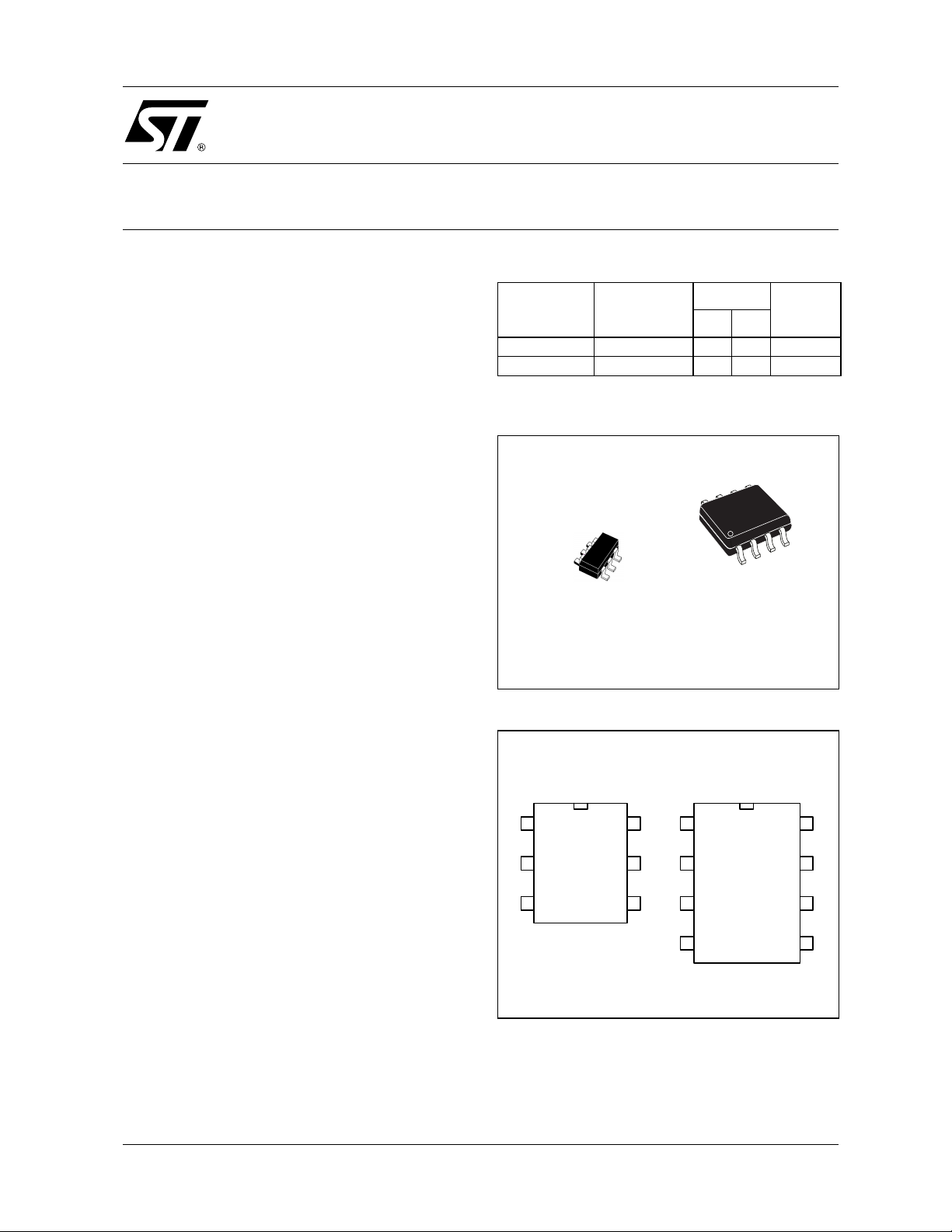
TSM1051, housed in one of the sma llest packa ge
available, is ideal for space shri nked applications
such as adapters and battery chargers.
APPLICATIONS
■ ADAPTERS
■ BAT TERY CHARGERS
ORDER CODE
Part Number
TSM1051CLT 0 to 85°C • M801
TSM1051CD 0 to 85°C • M1051C
L = Tiny Package (SOT23-6) - only available in Tape & Reel (LT)
D = Small Outline Package (SO) - also available in Tape & Reel ( DT)
(Plastic Package)
Temperature
Range
L
SOT23-6
Package
Marking
LD
D
SO8
(Plastic Micro package)
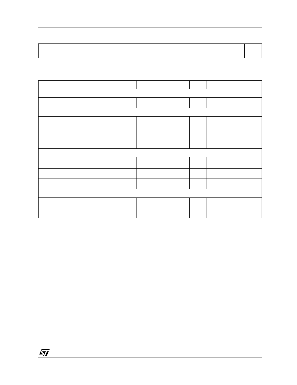
PIN CONNECTIONS (top view)
SOT23-6 SO8
1
2
Gnd
Vsense
34
Out Ictrl
6Vctrl
Vcc
1
5
2
3
45
Vctrl Gnd
Vcc
Vsense
Out
Ictrl
NcNc
8
7
6
January 2002
1/9

TSM1051
PIN DESCRIPTION
SOT23-6 Pinout
Name Pin # Type Function
Vcc 6 Power Supply Positive Power Supply Line
Gnd 2 Power Supply Ground Line. 0V Reference For All Voltages
Vctrl 1 Analog Input Input Pin of the Voltage Control Loop
Ictrl 4 Analog Input Input Pin of the Current Control Loop
Out 3 Current Sink Output Output Pin. Sinking Current Only
Vsense 5 Analog Input Input Pin of the Current Control Loop
SO8 Pinout
Name Pin # Type Function
Vcc 2 Power Supply Positive Power Supply Line
Gnd 8 Power Supply Ground Line. 0V Reference For All Voltages
Vctrl 1 Analog Input Input Pin of the Voltage Control Loop
Ictrl 6 Analog Input Input Pin of the Current Control Loop
Out 7 Current Sink Output Output Pin. Sinking Current Only
Vsense 3 Analog Input Input Pin of the Current Control Loop
NC 5
NC 4
ABSOLUTE MAXIMUM RATINGS
Symbol DC Supply Voltage Value Unit
Vcc DC Supply Voltage 14 V
Vi Input Voltage -0.3 to Vcc V
Top Operating Free Air Temperature Range 0 to 85 °C
Tj Maximum Junction Temperature 150 °C
Rthja Thermal Resistance Junction to Ambient SO8 package 130 °C/W
Rthja Thermal Resistance Junction to Ambient SOT23-6 package 250 °C/W
2/9
TSM1051
OPERATING CONDITIONS
Symbol Parameter Value Unit
Vcc DC Supply Conditions 2.5 to 12 V
ELECTRICAL CHARACTERISTICS
Tamb = 25°C and Vcc = +5V (unless otherwise specified)
Symbol Parameter Test Condition Min Typ Max Unit
Total Current Consumption
Icc Total Supply Current - not taking the
output sinking current into account
Voltage Control Loop
Gmv Transconduction Gain (Vctrl). Sink
Current Only
Vref
Voltage Control Loop Reference
1)
2)
Iibv Input Bias Current (Vctrl) Tamb
Current Control Loop
Gmi Transconduction Gain (Ictrl). Sink
Current Only
Vsense
Current Control Loop Reference
3)
4)
Iibi Current out of pin ICTRL at -200mV Tamb
Output Stage
Vol Low output voltage at 10 mA sinking
current
Ios Output Short Circuit Current. Output to
Vcc. Sink Current Only
1. If the vol tage on V CTRL (the negati ve input of the a m pl i fier) is hi gher than the pos i tive ampli f i er input (V ref=1.210V), and it is increased
by 1mV, the sinking current at the output OUT will be increased by 3.5mA.
2. The internal Voltage Reference is set at 1.210V (bandgap reference). The voltage control loop precision takes into account the cumulative
effects of the i nternal voltage reference dev i ation as well as the input offset voltage of th e trans- conductance operational amplifier. The
internal V ol tage Refer ence is fixed by bandgap, and trimmed to 0.5% accuracy at room temperature.
3. When the positive inp ut at ICTRL is lo wer than -200mV, and t he voltage i s decrease d by 1mV, the si nking current at the output OUT will
be increased by 7mA.
4. The internal current sense threshold is set to -200mV. The current control loop precision takes into account the cumulative effects of the
internal voltage ref erence deviation as wel l as the input of f set voltage o f the trans-c onduction operatio nal am plifier.
Tamb
0 < Tamb < 85°C
Tamb
0 < Tamb < 85°C
Tamb
0 < Tamb < 85°C
0 < Tamb < 85°C
T amb
0 < Tamb < 85°C
Iout = 2.5mA Tamb
0 < Tamb < 85°C
0 < Tamb < 85°C
Tamb
0 < Tamb < 85°C
Tamb
0 < Tamb < 85°C
1.1
2mA
1.2
1 3.5
mA/mV
2.5
1.198
1.186
1.21 1.222
1.234
50
100 nA
1.5 7 mA/mV
196
192
200 204
208
mV
25
50 µA
200 mV
27
35
50
mA
V
3/9

TSM1051
Figure 1 : Internal Schema t i c
1.210V
Vcc
Out
+
-
200mV
+
-
Gnd
Ictrl
Figure 2 : Typical Adapter or Battery Charger Application Using TSM1051
TSM1051
1.210V
200mV
+
Ictrl
Vcc
+
-
+
-
Gnd
Vsense
Out
Vsense
Rout
Cic1
2.2nF
Ric1
22K
To primary
Rvc1
470K
Cvc2
22pF
D
Cvc1
2.2nF
R2
R1
OUT+
IL
+
Load
Ric2
Vsense
Rsense
500
OUT-
IL
In the above application sche matic, the TSM1 051 is us ed o n the seco ndary s ide of a f lyback adapter (or
battery charger) to provide an accurate control of voltage and current. The above feedback loop is made
with an optocoupler.
4/9

TSM1051
Figure 3 : Vref vs Ambient Temperature
1,230
1,225
2,5V ≤ Vcc ≤ 12V
1,220
1,215
Vref (V)
1,210
1,205
1,200
0 20406080100120
Ta ambient t e mp er ature (°C)
Figure 4 : Vsense pin input bias current vs
Ambient Temperature
120
100
80
Vcc=12V
Figure 6 : Vsense vs Ambient Temperature
203,5
203,0
202,5
202,0
Vsense (V)
201,5
201,0
200,5
Vcc=2,5 V
Vcc=12V
0 20406080100120
Vcc=5V
Ta ambie nt temperature ( ° C )
Figure 7 : Ictrl pin input bias current vs
Ambient Temperature
30
28
26
Vcc=2,5V
60
Iibv (nA)
40
20
0
0 20 40 60 80 100 120
Vcc=5V
Vcc=2,5V
Ta ambient temper ature ( °C)
Figure 5 : Output short circuit current vs
Ambient Temperature
60
50
40
30
Ios (mA)
20
10
Vcc=12V
Vcc=5V
Vcc=2,5V
0
0 20406080100120
Ta ambient temperature (°C)
24
Iibi ( A)
22
20
18
0 20 40 60 80 100 120
Vcc=12V
Victrl=200mV
Ta ambient te m per at ur e ( ° C)
Vcc=5V
Figure 8 : Supply current vs Ambient
Temperature
1,6
1,4
1,2
1,0
0,8
Icc (mA)
0,6
0,4
0,2
0,0
Vcc=12V
Vcc=5V
Vcc=2,5V
0 20 40 60 80 100 120
Ta ambient temperat ur e (°C)
5/9

TSM1051
PRINCIPLE OF OPERATION AND APPLICATION HINTS
1. Voltage and Cu rren t Co ntrol
1.1. Voltage Control
The voltage loop is controlled via a first transc onductance operational am plifier, the resist or brid ge
R1, R2, and the optocoupler which is directly connected to the output.
The relation between the values of R1 and R2
should be chosen as written in Equation 1.
R1 = R2 x Vref / (Vout - Vref) Eq1
Where Vout is the desired output voltage.
To avoid the discharge of the load, the resistor
bridge R1, R2 should be h ighly resistive. For this
type of application, a total value of 100KΩ (or
more) would be appropriate for the resistors R1
and R2.
As an example, with R2 = 100K Ω, Vout = 4.10V,
Vref = 1.210V, then R1 = 41.9KΩ.
Note that if the low drop diode should be inserted
between the load and the voltage regulation resistor bridge to avoid current flowing from the load
through the resistor bridge, this drop should be
taken into account in the above calculations by replacing Vout by (Vout + Vdrop).
1.2. Current Control
The current loop is controlled via the second
trans-conductance operational amplifier, the
sense resistor Rsense, and the optocoupler.
The control equation verifies:
Rsense x Ilim = Vsense eq2
Rsense = V sens e / Ilim eq2’
where Ilim is the desired limited current, and
Vsense is the threshold voltage for the current
control lo op.
As an example, with Ilim = 1A, Vsense = -200mV,
then Rsense = 200mΩ.
Note that the Rsense resistor should be ch osen
taking into account the maximum dissipation
(Plim) through it during full load operation.
Plim = Vsense x Ilim. eq3
As an example, with Ilim = 1A, and Vsense =
200mV, Plim = 200mW.
Therefore, for most adapter and battery charger
applications, a quarter-watt, or half-watt resistor to
make the current sensing function is sufficient.
Vsense thresh old is achieved internally by a resistor bridge tied to the V ref voltage ref erence. Its
middle point is tied to the positive input of the current control operationa l ampli fier, an d its foot is to
be connected to lower potential point of the sense
resistor as shown on the following figure. The resistors of this bridge a re matched to provide the
best precision possible.
The current sinking outputs of the two trans-conductance operational amplifiers are common (to
the output of the IC). This makes an ORing function which ensures that whenever the c urrent or
the voltage reache s to o hi gh v alu es, the opt oc oupler is activated.
The relation between the controlled current and
the controlled output voltage can be described
with a square characteristic as shown in the following V/I output-power graph.
Figure 9 : Output voltage versus output current
Vout
Voltage regulation
TSM1051 Vcc : independent power supply
0
2. Compensation
The voltage-cont rol trans-conduct ance operational amplifier can be fully compensated. Both of its
output and negative inp ut are directly accessible
for external compensation components.
An example of a suitable compensation network is
shown in Fig.2. It consists of a capacitor
Cvc1=2.2nF and a resistor Rcv1=470KΩ in serie s,
Secondary current regulation
TSM1051 Vcc : On power output
Primary current regulation
Current regulation
Iout
6/9

TSM1051
connected in parallel with another capacitor
Cvc2=22pF.
The current-control trans-conductance operational amplifier can be fully compensated. Both of its
output and negative inp ut are directly accessible
for external compensation components.
An example of a suitable compensation network is
shown in Fig.2. It consists of a capacitor
Cic1=2.2nF and a resistor Ric1=22KΩ in series.
When the Vcc v oltage re aches 12V it c oul d be interesting to limit the current coming through the
output in the aim to reduce the dissipation of the
device and increase the stability performance s of
the whole application.
An example of a suitable Rout value could be
330Ω in series with the opto-coupler in case
Vcc=12V.
3. Start Up and Short Circuit Conditions
Under start-up or short-circuit conditions the
TSM1051 is not provided with a high enough supply voltage. This is due to the fact that the chip has
its power supply line in com mon with the power
supply line of the system.
Therefore, the current li mitation can only be ensured by the primary PWM m odule, which shoul d
be chosen accordingly.
If the primary current limitation is considered not to
be precise enough for the application, then a sufficient supply for the TSM 1051 has to be ensured
under any condition. It would then be nec essary
to add some circuitry to supply the chip with a separate power line. This can be achieved in numerous ways, including a n additional winding on the
transformer.
The following schematic shows how to realize a
low-cost power supply f or the TSM1051 (with no
additional windings).
Please pay attention to the fact that in the particular case presented here, this low-cost power supply can reach v oltages as high as twice t he voltage of the regulated line. Since the Absolute Maximum Rating of the TSM1051 supply voltage is 14
V, this low-cost auxiliary power supply can only be
used in applications whe re the regulated l ine volt age does not exceed 7 V.
Figure 10 :
Vcc
Rs
DS
CS
+
D
To primary
R2
TSM105
Vcc
1.210V
200mV
+
Ictrl
+
-
+
-
Vsense
Out
Gnd
Ric2
500
Vsense
Rout
Cic1
2.2nF
Ric1
22K
Cvc2
22pF
Rvc1
470K
Cvc1
2.2nF
R1
OUT+
IL
+
Load
OUT-
7/9
Rsense
IL

PACKAGE MECHANICAL DATA
6 PINS - PLASTIC PACKAGE SOT23-6
TSM1051
Dimensions
A 0.9 1.45 0.035 0.057
A1 0 0.15 0 0.006
A2 0.9 1.3 0.035 0.0512
B 0.35 0.5 0.0137 0.02
c 0.09 0.2 0.004 0.008
D 2.8 3 0.11 0.118
E 1.5 1.75 0.059 0.0689
e 0.95 0.0374
H 2.6 3 0.102 0.118
L 0.1 0.6 0.004 0.024
θ
Min. Typ. Max. Min. Typ. Max.
0 10 deg. 0 10 deg.
Millimeters Inches
8/9

TSM1051
PACKAGE MECHANICAL DATA
8 PINS - PLASTIC MICROPACKAGE (SO8)
Dim.
Millimeters Inches
Min. Typ. Max. Min. Typ. Max.
A 1.75 0.069
a1 0.1 0.25 0.004 0.010
a2 1.65 0.065
a3 0.65 0.85 0.026 0.033
b 0.35 0.48 0.014 0.019
b1 0.19 0.25 0.007 0.010
C 0.25 0.5 0.010 0.020
c1 45° (typ.)
D 4.8 5.0 0.189 0.197
E 5.8 6.2 0.228 0.244
e 1.27 0.050
e3 3.81 0.150
F 3.8 4.0 0.150 0.157
L 0.4 1.27 0.016 0.050
M 0.6 0.024
S 8° (max.)
Information furnished is bel ieved to be accurate and reliable. However, STMicroe lectronics assumes no responsibility for the
consequences of use of such information nor for any infringement of patents or other rights of third parties which may result from
its use. No li cense is granted by i mp lica tion or otherwise under a n y patent or patent rig hts of STMicroelectronics. Spec ific at ions
mentioned in this publication ar e subject to change without notice. This publication supersedes and replaces all information
previously supplied. S TMicroelectronics products are not authorized for use as critica l components in life suppo rt devices or
systems without express written approval of STMicroelectronics.
© The ST logo is a registered trademark of STMicroelectronics
9/9
© 2002 STM icroelectronics - Printed in Italy - All Ri g h ts Reserv ed
STMicr o el ectronics G ROU P OF COMPANI E S
Australi a - Brazil - Canada - Chin a - F i nland - France - Germany - Hong Ko ng - India - Israel - Italy - Japan - Malaysia
Malta - Mor occo - Singapore - Spai n - Sweden - S wi t zerland - U n i t ed Kingdom - United Sta tes
© http://www.st.com
 Loading...