

SGS Thomson Microelectronics TSM105, TSM105CLT, TSM105CDT, TSM105CD Datasheet
1/9
■ CONSTANT VOLTAGE AND CONSTANT
CURRENT CONTROL
■ LOW VOLTAGE OPERATION
■ PRECISION INTERNAL VOLTAGE REFER-
ENCE
■ LOW EXTERNAL COMPONENT COUNT
■ CURRENT SINK OUTPUT STAGE
■ EASY COMPENSATION
■ LOW AC MAINS VOLTAGE REJECTION
DESCRIPTION
TSM105 is a hi ghly integrated solut ion for SMPS
applications requiring CV (cons tant voltage) and
CC (constant current) mode.
TSM105 integrates one voltage reference, two
operational amplifiers (with OR ed outputs - common collectors), and a current sensing circuit.
The voltage reference combined with one operational amplifier mak es it an ideal voltage cont roller, and the other low voltage reference combined
with the other operational amplifier makes it an
ideal current limiter for output low side current
sensing.
The current threshold is fixed, and precise.
The only external components are:
* a resistor bridge to be connected on the output of
the power supply (adapter, battery charg er) to set
the voltage regulation by dividing the desired output voltage to match the internal v oltage reference
value.
* a sense resistor whos e valu e and allowable dissipation power need to be chosen according to the
internal voltage threshold.
* optional compensation components (R and C).
TSM105, housed in o ne of the smallest package
available, is ideal for space shri nked applications
such as adapters and battery chargers.
APPLICATIONS
■ ADAPTERS
■ BAT TERY CHARGERS
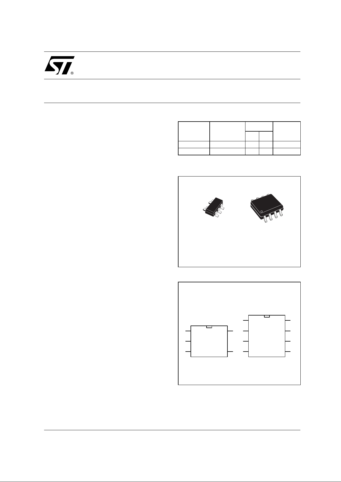
ORDER CODE
L = Tiny Package (SOT23-5) - only available in Tape & Reel (LT)
D = Small Outline Package (SO) - also available in Tape & Reel (DT)
PIN CONNECTIONS (top view)
Part
Number
Temperature
Range
Package
Marking
LD
TSM105CLT 0 to 85°C • M105
TSM105CD 0 to 85°C • TSM105
L
SOT23-5
(Plastic Package)
D
SO8
(Plastic Micropackage)
1
2
34
5Vctrl
Gnd
Vcc
IctrlOut
1
2
3
45
6
Vctrl Gnd
Vcc
Nc
Out
Ictrl
Nc
Nc
SOT23-5
SO8
7
8
September 2001
TSM105
CONSTANT VOLTAGE AND CONSTANT CURRENT
CONTROLLER FOR BATTERY CHARGERS AND ADAPTORS
TSM105
2/9
PIN DESCRIPTION
SOT23-5 Pinout
SO8 Pinout
ABSOLUTE MAXIMUM RATINGS
Name Pin # Type Function
Vcc 5 Power Supply Positive Power Supply Line
Gnd 2 Power Supply Ground Line. 0V Reference For All Voltages
Vctrl 1 Analog Input Input Pin of the Voltage Control Loop
Ictrl 4 Analog Input Input Pin of the Current Control Loop
Out 3 Current Sink Output Output Pin. Sinking Current Only
Name Pin # Type Function
Vcc 2 Power Supply Positive Power Supply Line
Gnd 8 Power Supply Ground Line. 0V Reference For All Voltages
Vctrl 1 Analog Input Input Pin of the Voltage Control Loop
Ictrl 6 Analog Input Input Pin of the Current Control Loop
Out 7 Current Sink Output Output Pin. Sinking Current Only
NC 3
NC 4
NC 5
Symbol DC Supply Voltage Value Unit
Vcc DC Supply Voltage 14 V
Vi Input Voltage -0.3 to Vcc V
Top Operating Free Air Temperature Range -55 to 125 °C
Tj Maximum Junction Temperature 150 °C
Rthja Thermal Resistance Junction to Ambient SO8 package 130 °C/W
Rthja Thermal Resistance Junction to Ambient SOT23-5 package 250 °C/W
TSM105
3/9
OPERATING CONDITIONS
ELECTRICAL CHARACTERISTICS
Tamb = 25°C and Vcc = +5V (unless otherwise specified)
Symbol Parameter Value Unit
Vcc DC Supply Conditions 2.8 to 12 V
Symbol Parameter Test Condition Min Typ Max Unit
Total Current Consumption
Icc Total Supply Current - not taking the
output sinking current into account
Tamb
0 < Tamb < 85°C
1.05
1.2
2mA
Voltage Control Loop
Gmv Transconduction Gain (Vctrl). Sink
Current Only
1)
1. If the vol tage on VCTRL (the negative input of th e amplifier) is high er than the positive am pl i fier input (Vref=1. 210V), and it is increased
by 1mV, the sinking current at the output OUT will be increased by 3.5mA.
Tamb
0 < Tamb < 85°C
1 3.5
2.5
mA/mV
Vref
Voltage Control Loop Reference
2)
2. The internal Voltage Reference is set at 1.210V (bandgap reference). The voltage control loop precision takes into account the cumulative
effects of the internal voltage reference deviation as we l l as the i nput offs et volta ge of the trans-conductance operati onal amplifier . The
internal V ol t age Referen ce is fixed by bandgap, and trimm ed to 0.5% accuracy at room temperaure.
Tamb
0 < Tamb < 85°C
1.198
1.186
1.21 1.222
1.234
V
Iibv Input Bias Current (Vctrl) Tamb
0 < Tamb < 85°C
50
100
nA
Current Control Loop
Gmi Transconduction Gain (Ictrl). Sink
Current Only
3)
3. When the positive input at ICTRL is lower than -20 0mV, and the vol t age is decreased by 1mV, t he sinking cur rent at the out put OUT will
be increased by 7mA.
T amb
0 < Tamb < 85°C
1.5 7
4
mA/mV
Vsense
Current Control Loop Reference
4)
4. The internal current sense threshold is set to -200mV. The current control loop precision takes into account the cumulative effects of the
internal vo l tage reference deviation as well as the in put offset volta ge of the trans -c onductance operational am plifier.
Iout = 2.5mA Tamb
0 < Tamb < 85°C
196
192
200 204
208
mV
Iibi Current out of pin ICTRL at -200mV Tamb
0 < Tamb < 85°C
25
50
µA
Output Stage
Vol Low output voltage at 10 mA sinking
current
Tamb 200 mV
Ios Output Short Circuit Current. Output to
Vcc. Sink Current Only
Tamb
0 < Tamb < 85°C
27
35
50 mA
 Loading...