

Datasheet TSI62B1, TSI265B1, TSI200B1, TSI220B1, TSI180B1 Datasheet (SGS Thomson Microelectronics)

TSIxxB1
®
Telecom equipment requiring combin ed
protection against transient overvoltages and
rectification by diode bridge :
Telephone set
Base station for cordless s et
Fax machine
Modem
Caller Id equipment
Set top box
MAIN APPLICATION
SO8
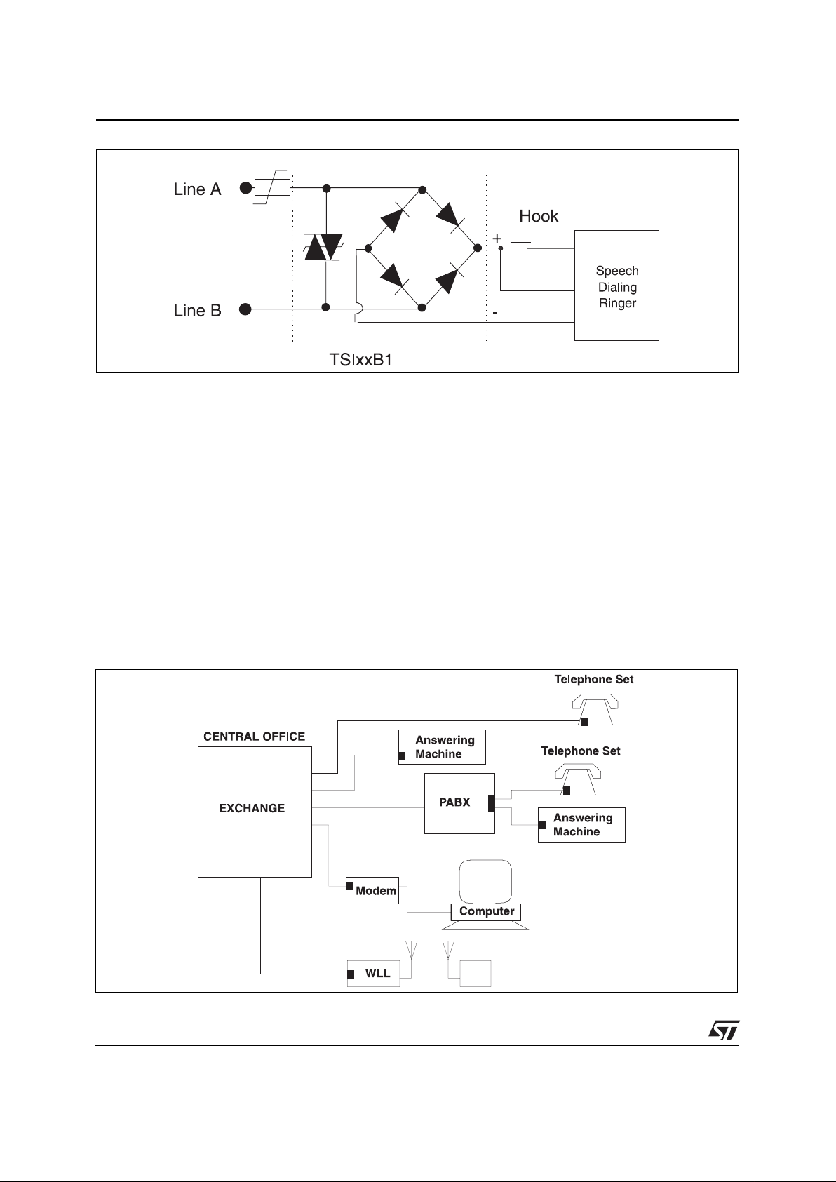
The TSIxxB1 provides the diode bridge and the
crowbar protection function that can be found in
most of telecom terminal equipment.
Integrated monolithically within a SO8 package,
this ASD device allows space saving on the
board and greater reliability.
DESCRIPTION
CCITT K17 - K20
10/700µs 1.5 kV
5/310µs 38A
VDE 0433
10/700µs2 kV
5/310µs 40A(*)
CNET
0.5/700µs 1.5 kV
0.2/310µs 38A
Bellcore
TR-NWT-000974
: 10/1000µs1 kV
10/1000µs 30A(*)
FCC Part 68
2/10µs 2.5 kV
2/10µs 75A (*)
MIL STD883C Method 3015-6
(*) with series resistor or PTC.
IN ACCORDANCE WITH THE FOLLOWING
STANDARDS :
SCHEMATIC DIAGRAM
TERMINAL SET INTERFACE
PROTECTION AND DIODE BRIDGE
January 1998 - Ed: 3
Diode bridge for polarity guard and crowbar
protection within one device.
Single chip for greater reliability
Reduces component count versus discrete
solution
Saves space on the board
BENEFITS
STAND-OFF VOLTAGE FROM 62V TO 265V
PEAK PULSE CURRENT : 30 A (10/1000 µs)
MAXIMUM DC CURRENT : IF = 0.2 A
HOLDING CURRENT :150 mA
FEATURES
Application Specific Discretes
A.S.D.
TM: ASD is trademarks of SGS-THOMSON Microelectronics.
2
3
1
4
7
6
8
5
1/9
PTC
TYPICAL APPLICATION
Telecom terminals have a diode bridge for polarity
guard, located at the line interface stage. They also
have above this diode bridge one crowbar
protection device that is mandatory to prevent
atmospheric effects and AC mains disturbances
from damaging the electronic circuitry that follows
the diode bridge.
SGS-THOMSON proposes a one chip device that
includes both protection and diode bridge. This is
the concept of the T SIxxB1 dev ices.
Fig. 1 : The various uses of the TSIxxB1 in a conventional telecom network
TSIxxB1
2/9

The VRM value corresponds to the maximum
voltage of the application in normal operation. For
instance, if the maximum line voltage is ranging
between ±100V
RMS
of ringing plus 48V of battery
voltage, then the protection chosen for this application shall have a V
RM
close to 200V.
The V
BO
is the triggering voltage. This indicates the
voltage limit for which the component
short-circuits. Passing this V
BO
makes the device
turn on.
The I
BO
is the current that makes the device t urn
on. Indeed, if we want a Trisil to be turned on not
only the voltage across it shall pass the V
BO
value
but the current through it shall also pass the I
BO
value.
In other words, if a voltage surge occurring on the
line is higher than the V
BO
value of a Trisil, whereas
the line surge current is limited to a value that does
not exceed the Trisil’s I
BO
value, then the Trisil will
never turn into short circuit. At this time the surge
will be
clamped by the Trisil.
Anyhow the electronic circuitry located after the
Trisil will always be protected whatever the Trisil
state is (crowbar or clamping mode).
The I
H
stands for the holding current. When the
Trisil is turned on, as soon as the crossing current
surge gets lower than this I
H
value, the Trisil
protection device turns back in its idle state.
Remark : for this r eason the Trisil ’s IH value shall
be chosen higher than what the maximum t elecom
line current can be.
TSIxxB1 BEHAVIOUR WITH REGARD TO
SURGE STANDARD :
The TSIxxB1 is able to replac e both diode bridge
and usual discrete protection on telecom
terminals. Furthermore it complies with the CCITT
K17 recommendations :
10/700 µs waveform surge test, ± 1.5kV
AC power induction test
AC power contact test
ELECTR ICAL PAR AME TERS
Ω
Fig. 2 : Test circuit for the CCITT K17 recommendations
TSIxxB1
3/9

This test concerns the 10/700 µs waveform surge,
± 1.5 kV.
The surge generator used for the test has the
following circuitry (fig.2).
TEST # 1
LIGHTNING SIMULATION
Ω
Ω
Ω
Fig. 2 : 10/700 µs waveform surge generator circuit
The behaviour of the TSI200B1 to this lightning surge is given below (fig. 3).
Fig. 3 : Voltage across the TSI200B1 at the + and - terminations and current throught it
for a 1.5 kV positive surge (fig.3a) and negative surge (fig. 3b)
These curves show the peak voltage the surge
generates across the TSI200B1 + and terminations. This lasts a short time (≈ 2 µs) and
after, as the internal protection gehaves like a short
circuit. The voltage drop across the TSIxxB1
becomes a few volts. In the meanwhile all the
surge current flows in the protection.
As far as the 10/700 µs waveform surge test is
concerned,the TSIxxB1 withstand the ± 1.5 kV
test.
TSIxxB1
4/9

This test simulates the induction phenomena that
can happen between telecom lines and AC mains
lines (fig. 4).
TEST # 2
AC POWE R INDUCTION TEST
Fig. 4 : AC power induction test circuit
Part #1
test conditions : V
RMS
= 240 V
R = 600 Ω
t = 0.2 s
Part #2
test conditions : V
RMS
= 600 V
R = 600 Ω
t = 0.2 s
Fig. 5 : Voltage at the + and - terminations of the
TSI200B1, and current through it
while test part 1 is applied.
The TSIxxB1 withstand the AC power induction
test in both cases.
This test simulates the direct contact between the
telecom lines and the AC mains lines.
The AC power contact test consists in applying
240V
RMS
through a 10Ω PTC during 15 minutes
long on the device under test. The CCITT K17
recommendation specifies an internal generator
impedance allowing 10 A
RMS
when in short circuit.
The behavior of the TSI200B1 with respect to this
surge is given in figure 6.
TEST #3
AC POWER CONTACT TEST
Fig. 6 : Voltage at the TSI200B1 + & - terminations
and the current through it.
The figure 6 shows that after 250ms there is no
current anymore flowing through the TSI200B1
device. This is due to the action of the serial PTC
that limits the current through the line. This PTC is
mandatory for this test. It can also be replaced by a
fuse or any other serial protection that "opens" the
line loop under AC contact test.
TSIxxB1
5/9

Symbol Parameter Value Unit
I
PP
Non repetitive peak on-sate current (see note 1)
10/1000 µs (open circuit voltage wave shape 10/100 µs)
5/310 µs (open circuit voltage wave shape 10/700 µs)
2/10 µs (open circuit voltage wave shape 2/10 µs)
30
40
75
A
I
F
Maximu m DC cur rent
0.2 A
I
TSM
Non repetitive surge peak on-state current tp = 20 ms
t = 1s
5
3.5
A
T
stg
T
j
Storage temperature range
Maximum junction temperature
- 55 to +150
150
°C
T
L
Maximum lead temperature for soldering during 10 s 260 ° C
ABSOL UTE M AXIMU M RA TIN GS (T
amb
= 25°C)
Note 1 :
Pulse wa vef orm :
10/1000µstr=10µst
p
=1000µs
5/310µst
r
=5µst
p
=310µs
2/10µst
r
=2µst
p
=10µs
100
50
%I
PP
t
t
r
p
0
t
Symbol Parameter Value Unit
R
th(j -a )
Junction to ambient 170 °C/ W
THERMAL RE SISTA NC E
Symbol Parameter
V
RM
Stand-off voltage
V
BO
Breakover voltage
V
BR
Breakdown voltage
I
H
Holding current
I
BO
Breakover current
I
RM
Leakage current at V
RM
I
PP
Peak pulse current
C Capacitance
αT Temperature coefficient
ELECTRICAL CHARACTERI STICS (T
amb
=25°C )
V
I
V
RM
BO
V
RM
I
H
I
BO
PP
I
I
TSIxxB1
6/9

Type
I
RM
@ V
RM
VBO @ I
BO
I
H
I
BO
C
note1 note2 note1 note3
µAV V mA mAmApF
max. max. min. min. max. typ.
TSI6 2B 1
1
5
50
62
90 150 50 400 200
TSI180B1
1
5
50
180
250 150 50 400 200
TSI200B1
1
5
50
200
290 150 50 400 200
TSI220B1
1
5
50
220
330 150 50 400 200
TSI265B1
1
5
50
265
380 150 50 400 200
Note 1 :
Measured at 50 Hz, one cycle
Note 2 :
See test cricuit
Note 3 :
VR = 0V, F = 1MHz, between pins 1 and 8.
ELECTRICAL CHARACTERI STICS (T
amb
= 25 °C)
1 - PROTECTION DEVICES PARAMETERS
Symbol Test condition Value Unit
V
F
(for one diode)
I
F
= 20 mA
I
F
= 100 mA
0.9
1.1
V
V
2 - DIODE BRIDGE PARAMETERS
FUNCTIONAL HOLDING CURRENT (IH) TEST CIRCUIT : GO - NO GO TEST
This is a GO-NOGO Test which allows to confirm the holding current (I
H
) level in a functional
test ci rc u it.
TEST PROCEDURE :
1) Adjust the current level at the IH value by short circuiting the D.U.T.
2) Fire the D.U.T with a surge Current : Ipp = 10A , 10/1000 µs.
3) The D.U.T will come back off-state within a duration of 50 ms max.
R
-V
P
V
BAT
=-48V
Surge generator
D.U.T.
TSIxxB1
7/9

Type Marking
TSI62B1 TSI62
TSI180B1 TSI180
TSI200B1 TSI200
TSI220B1 TSI220
TSI265B1 TSI265
MARKING
ORDER CODE
RL = tape& reel ( 2500 pc s) .
= tube (100 pcs).
SO8 Package
TSI
265
B
1
RL
V
BR min.
Terminal
Set
Interface
TSIxxB1
8/9

Packagin g : prod uct su pplie d in tap e and ree l or anti stat ic tube s.
Information furnished is believed to be accurate and reliable. However, STMicroelectronics assumes no responsibility for the conseq ue nces o f
use of such information nor for any infringement of patents or other rights of third parties which may result from its use. No license is granted by
implication or otherw ise under any pa tent or patent ri ghts of STMi croelec tronics. Spec ifications mentione d in this pub lication are su bject to
change without notice. This publication supersedes and replaces all information previously supplied.
STMicroelectr oni cs products are n ot au thorized for use as critical components in life support devi ces or systems wi t hout express written approval of STMicroelectronics.
© 1998 STMicroelectronics - Printed in Italy - All rights reserved.
STMicroelectronics GROUP OF COMPANIES
Australia - Brazil - Canada - China - France - Germany - Italy - Japan - Korea - Malaysia - Malta - Mexico - Morocco - The
Netherlands - Singapore - Spain - Sweden - Switzerland - Taiwan - Thailand - United Kingdom - U.S.A.
PACKAGE MECHANICAL DAT A
SO8
REF. DIMENSIONS
Millimetres Inches
Min. Typ. Max. Min. Typ. Max.
A 1.75 0.069
a1 0.1 0.25 0.004 0.010
a2 1.65 0.065
b 0.35 0.48 0.014 0.019
b1 0.19 0.25 0.007 0.010
C 0.50 0.020
c1 45° (typ )
D 4.8 5.0 0.189 0.197
E 5.8 6.2 0.228 0.244
e 1.27 0.050
e3 3.81 0.150
F 3.8 4.0 0.15 0.157
TSIxxB1
9/9
 Loading...