

HIGH SPEED LOW POWERQUAD OPERATIONAL
AMPLIFIER WITH DUAL STANDBY POSITION
.
2 SEPARATESTANDBY : REDUCED
CONSUMPTION AND HIGHIMPEDANCE
OUTPUTS
.
LOW SUPPLYCURRENT : 4.5mA/amp.typ.
.
HIGHSPEED: 150MHz - 110V/µs
.
UNITYGAIN STABILITY
.
LOW OFFSETVOLTAGE : 4mV
.
LOW NOISE4.2 nV/√Hz
.
LOW COST
.
SPECIFIEDFOR 600Ω AND 150Ω LOADS
.
HIGHVIDEOPERFORMANCES :
Differential Gain: 0.03%
DifferentialPhase : 0.07
Gain Flatness : 6MHz, 0.1dB max. @ 10dB
gain
.
HIGHAUDIO PERFORMANCES
.
ESD TOLERANCE : 2kV
.
SPICEMACROMODEL INCLUDEDIN THIS
SPECIFICATION
o
N
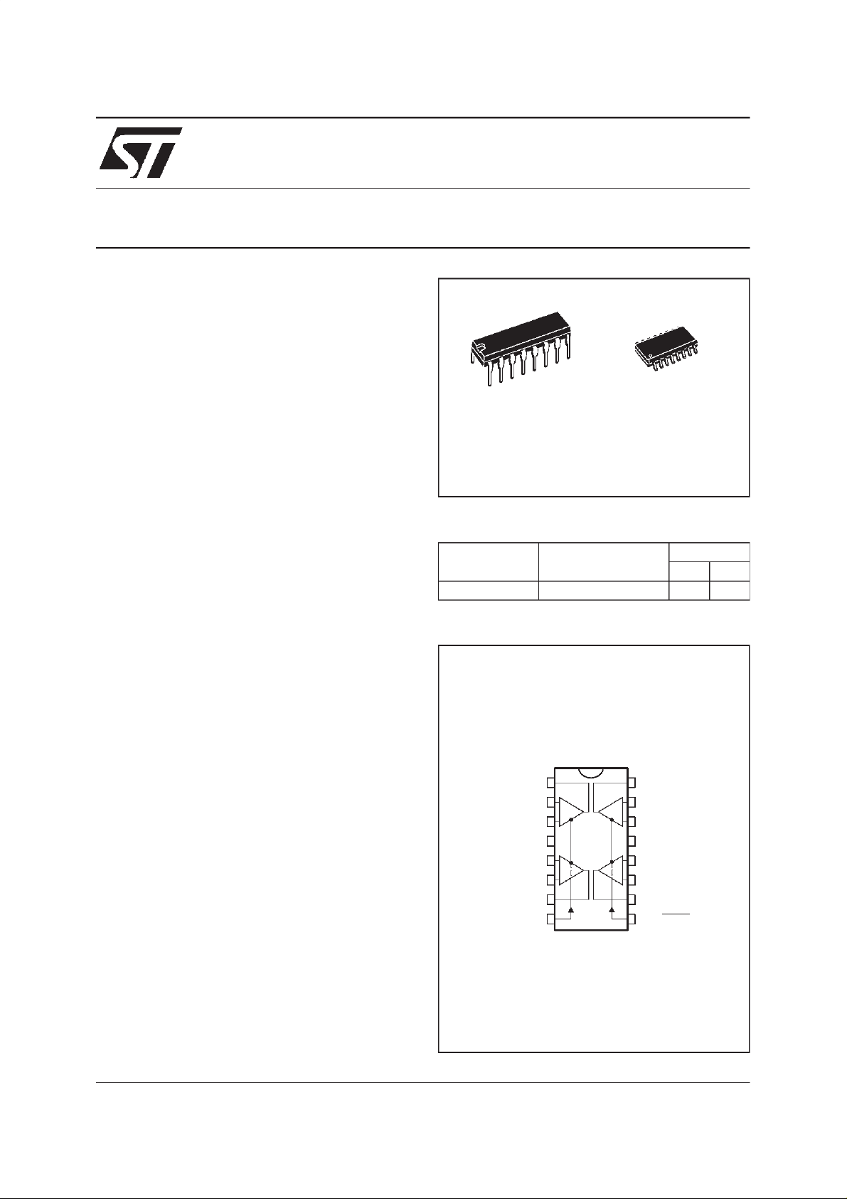
DIP16
(Plastic Package)
ORDER CODES
Part Number Temperature Range
TSH95I -40, +125
(Plastic Micropackage)
o
C ••
TSH95
D
SO16
Package
ND
DESCRIPTION
The TSH95 is a quad low power high frequency
op-amp, designed for high quality video processing.Thedeviceoffersan excellent speedconsumption ratio with 4.5mA per operator for 150MHz
bandwidth.
High slew rate and low noise make it suitable for
high quality audio applications.
The TSH95 offers 2 separate complementary
STANDBY pins :
• STANDBY1 acting on both n° 1 & 2 operators
• STANDBY2 acting on both n° 3 & 4 operators
Theyreducetheconsumptionofthecorresponding
operatorsandput their output ina high impedance
state.
PIN CONNECTIONS (top view)
Output 1
Inverting Input 1
Non-inve rting Input 1
Non-inve rting Input 2
Inverting Input 2
Output 2
Standby 1
1
2
-
+
3
+
4
V
CC
5
+
-
6
7
8
-
+
+
-
16
Output 4
15
Inverting Input 4
14
Non-inve rting Input 4
-
V
13
CC
12
Non-inve rting Input 3
Inverting Input 3
11
Output 3
10
Standby 2
9
November 1998
1/11
TSH95
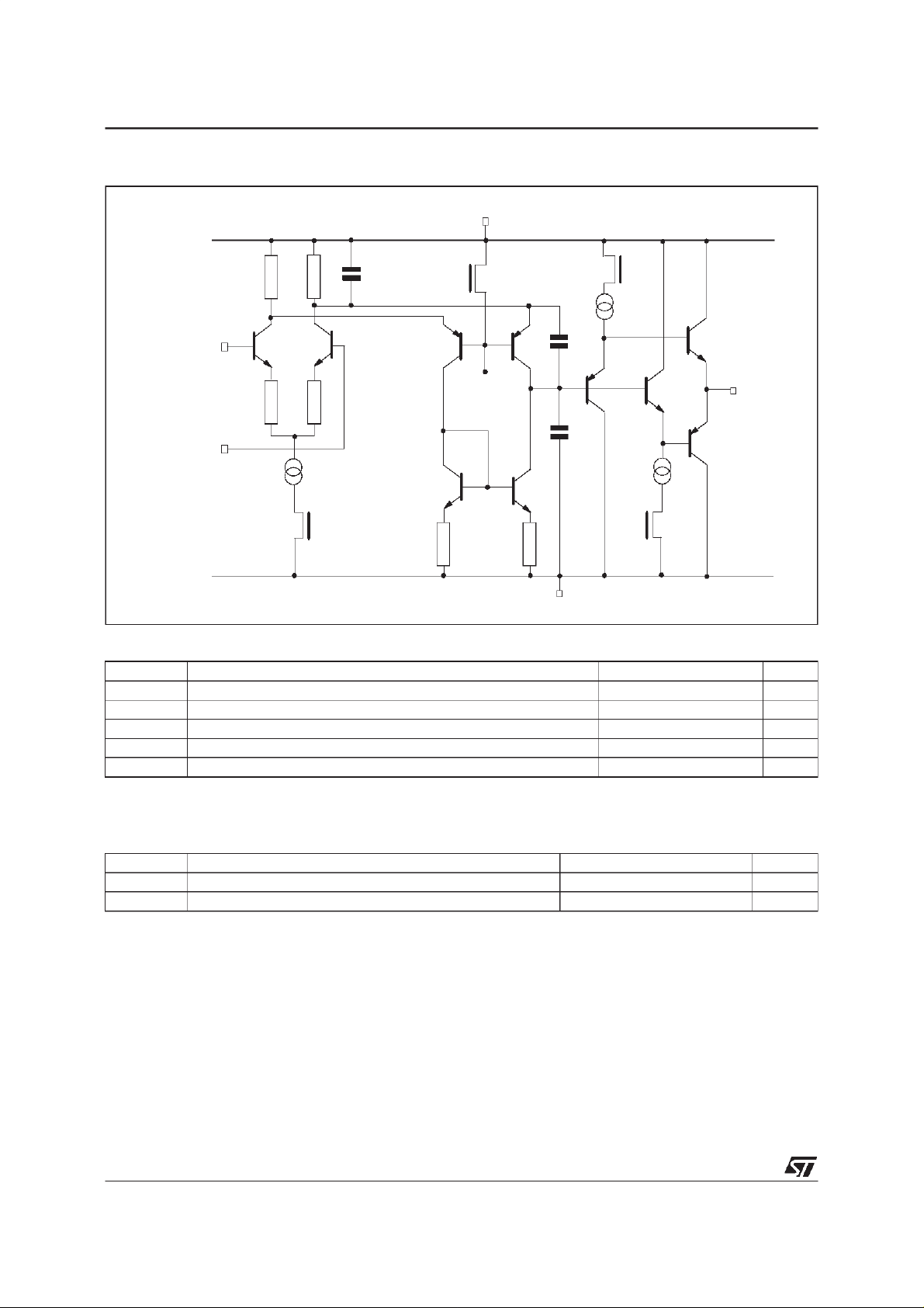
SCHEMATIC DIAGRAM
+
V
CC
stdby
stdby
non inverting
input
inverting
input
stdby
Internal
V
ref
C
c
stdby
-
V
CC
output
ABSOLUTE MAXIMUMRATINGS
Symbol Parameter Value Unit
V
CC
V
id
V
T
oper
T
stg
Notes : 1. All voltage values, except differential voltage are withrespect to network ground terminal.
Supply Voltage - (note 1) 14 V
Differential Input Voltage - (note 2) ±5V V
Input Voltage - (note 3) -0.3 to 12 V
i
Operating Free Air Temperature Range -40 to +125
Storage Temperature -65 to +150
2. Differential voltages are the non-inverting input terminal with respect to the inverting input terminal.
3. The magnitude of input and output voltages must never exceed V
CC
+
+0.3V.
OPERATING CONDITIONS
Symbol Parameter Value Unit
V
CC
V
icm
Supply Voltage 7 to 12 V
Common Mode Input Voltage Range V
CC
-
+2V to V
+
-1 V
CC
o
C
o
C
2/11
TSH95
ELECTRICAL CHARACTERISTICS
+
=5V,V
V
CC
(unlessotherwisespecified)
Symbol Parameter Min. Typ. Max. Unit
V
io
I
io
I
ib
I
CC
CMR Common Mode Rejection Ratio (V
SVR Supply Voltage Rejection Ratio (V
A
vd
V
OH
V
OL
I
o
GBP Gain Bandwidth Product
f
T
SR Slew Rate (A
∅m Phase Margin (A
e
n
V
O1/VO2
Gf Gain Flatness (f = DC to 6MHz, A
THD Total Harmonic Distortion (f = 1kHz, V
∆G Differential Gain (f = 3.58MHz, A
∆
ϕ
-
=-5V, pin 8 connectedto 0V,pin 9 connectedto V
CC
Input Offset Voltage (Vic=Vo= 0V)
≤ T
T
min.
amb.
≤ T
max.
Input Offset Current
≤ T
T
min.
amb.
≤ T
max.
Input Bias Current
≤ T
T
min.
amb.
≤ T
max.
Supply Current (per amplifier, no load)
≤ T
≤ T
≤ T
amb.
amb.
amb.
≤ T
≤ T
≤ T
max.
max.
max.
= -3V to +4V, Vo= 0V)
ic
= ±5V to ±3V)
CC
T
min.
T
min.
T
min.
Large Signal Voltage Gain (RL= 10kΩ,VO=±2.5V)
≤ T
T
min.
amb.
≤ T
max.
CC
+
,T
amb
80
70
60
50
57
54
=25oC
4
6
12
5
51520µA
4.5 6
8
100 dB
75 dB
70 dB
mV
µA
mA
High Level Output Voltage (Vid= 1V)
= 600Ω
R
L
= 150Ω
R
≤ T
T
min.
amb.
≤ T
max.
L
RL= 150Ω
3
2.5
2.4
3.5
3
Low Level Output Voltage (Vid= -1V)
= 600Ω
R
L
= 150Ω
R
≤ T
T
min.
amb.
≤ T
max.
L
RL= 150Ω
Output Short Circuit Current (Vid= ±1V) Source
Sink
≤ T
T
min.
amb.
≤ T
max.
Source
Sink
20
20
15
15
-3.5
-2.8
36
40
-3
-2.5
-2.4
mA
MHz
= 100, RL= 600Ω,CL= 15pF, f =7.5MHz) 90 150
(A
VCL
Transition Frequency 90 MHz
= +1, RL= 600Ω,CL= 15pF, Vin= -2 to +2V) 62 110 V/µs
VCL
= +1) 35 Degrees
VM
Equivalent Input Noise Voltage (Rs=50Ω, f = 1kHz) 4.2
nV
√Hz
Channel Separation (f = 1MHz to 10MHz) 65 dB
= 10dB) 0.1 dB
VCL
= ±2.5V, RL= 600Ω) 0.01 %
o
= +2, RL= 150Ω) 0.03 %
VCL
DifferentialPhase (f = 3.58MHz, A
= +2, RL= 150Ω)
VCL
0.07 Degree
V
V
3/11
TSH95
STANDBY MODE V
CC
+
=5V,V
Symbol Parameter Min. Typ. Max. Unit
V
SBY
Pin 8/9 Threshold Voltage for STANDBY Mode V
CC
-
=-5V, T
=25oC (unless otherwisespecified)
amb
+
-2.2 V
CC
CC
+
-1.6 V
+
-1.0 V
CC
Total Consumption
I
CC SBY
I
sol
t
ON
t
OFF
I
D
I
OL
I
IL
Pin 8 (Standby 1) = 0, Pin9 (Standby2)= 0
Pin 8 (Standby 1) = 1, Pin9 (Standby2)= 1
Pin 8 (Standby 1) = 1, Pin9 (Standby2)= 0
Input/Output Isolation (f = 1MHz to 10MHz) 70 dB
Time from Standby Mode to Active Mode 200 ns
Time from Active Mode to Standby Mode 200 ns
Standby Driving Current 2 pA
Output Leakage Current 20 pA
Input Leakage Current 20 pA
9.4
9.4
0.8
LOGIC INPUT STATUS
Standby 1 Standby 2 Op-amp 1 & 2 Op-amp 2 & 3
0 0 Enable Standby
0 1 Enable Enable
1 0 Standby Standby
1 1 Standby Enable
STANDBY POSITION
V
CC
sta ndby
STANDBY MODE
To put the devicein standby,justapplya logic level
on the standby MOS input. As ground is a virtual
level for the device, threshold voltage has been
referedto V
CC
+
at V
+
- 1.6V typ.
CC
In standby mode, the output goes in high impedance in 200ns. Be aware that all maximum rating
muststill be followedinthis mode. It leadsto swing
limitationwhileusingthe devicein signalmultiplexing configuration with followers, differential input
V
CC
voltage must not exceed ±5V limiting input swing
to 2.5Vpp.
mA
APPLICATIONS
SIGNAL MULTIPLEXING SAMPLEAND HOLD
4/11

PRINTEDCIRCUIT LAYOUT
TSH95
As for any high frequency device,a few rules must
be observed when designing the PCB to get the
best performancesfrom this high speed op amp.
From the most to the least important points :
•
Each power supply lead has to be by-passedto
ground with a 10nF ceramic capacitor very
close to the device and 10µF capacitor.
•
To provide low inductance and low resistance
common return, use a ground plane or common
point return for power and signal.
INPUT OFFSET VOLTAGE DRIFT VERSUS
TEMPERATURE
•
All leads must be wide and as short as possible
especially for op amp inputs. This is in order to
decreaseparasiticcapacitance and inductance.
•
Use small resistor values to decreasetime constant with parasitic capacitance.
•
Choose component sizes as small as possible
(SMD).
•
On output, decrease capacitor load so as to
avoid circuit stability being degraded which may
cause oscillation. You can also add a serial resistorin order to minimise its influence.
STATIC OPENLOOP VOLTAGEGAIN
LARGE SIGNALFOLLOWER RESPONSE SMALLSIGNAL FOLLOWERRESPONSE
5/11

TSH95
OPEN LOOP FREQUENCY RESPONSE AND
PHASESHIFT
AUDIO BANDWIDTH FREQUENCY
RESPONSEAND PHASE SHIFT
(TSH95 vs Standard 15MHz Audio Op-Amp)
CLOSELOOP FREQUENCY RESPONSE
GAIN FLATNESS AND PHASE SHIFT VERSUS
FREQUENCY
CROSS TALK ISOLATION VERSUS
FREQUENCY (SO16 PACKAGE)
6/11
CROSSTALK ISOLATION VERSUS
FREQUENCY (SO16 PACKAGE)

TSH95
INPUT/OUTPUT ISOLATION IN STANDBY
MODE (SO16 PACKAGE)
SIGNALMULTIPLEXING (cf p. 4)
STANDBY SWITCHING
DIFFERENTIAL INPUT IMPEDANCE VERSUS
FREQUENCY
4.5
4.0
3.5
3.0
2.5
2.0
Zin-diff(kΩ)
1.5
1.0
0.5
1k 10k 100k 1M 10M 100M
COMMONINPUT IMPEDANCE VERSUS
FREQUENCY
120
100
80
60
Zin-com (MΩ)
40
20
1k 10k 100k 1M 10M 100M
Fre quency (Hz)
Frequency (Hz)
7/11

TSH95
MACROMODEL
.
LOW DISTORTION
.
GAIN BANDWIDTH PRODUCT : 150MHz
Applies to : TSH95,I
** Standard Linear Ics Macromodels, 1996.
** CONNECTIONS :
* 1 INVERTING INPUT
* 2 NON-INVERTING INPUT
* 3 OUTPUT
* 4 POSITIVEPOWERSUPPLY
* 5 NEGATIVE POWER SUPPLY
* 6 STANDBY
.SUBCKT TSH95 1 3 2 4 5 6 (analog)
**********************************************************
**************** switch *******************
.SUBCKT SWITCH 20 10 INOUT COM
.MODEL DIDEAL D N=0.1 IS=1E-08
DP IN 1 DIDEAL 400E-12
DN OUT 2 DIDEAL 400E-12
EP 1 OUT COM 10 2
EN 2 IN COM 10 2
RFUIT1 IN 1 1E+09
RFUIT2 OUT 2 1E+09
RCOM COM 0 1E+12
.ENDS SWITCH
**************** inverter *****************
.SUBCKT INV 20 10 IN OUT
.MODEL DIDEAL D N=0.1 IS=1E-08
RP1 20 15 1E+09
RN1 15 10 1E+09
RIN IN 10 1E+12
RIP IN 20 1E+12
DPINV OUT 20 DIDEAL 400E-12
DNINV 10 OUT DIDEAL 400E-12
GINV 0 OUT IN 15 -6.7E-7
CINV 0 OUT 210f
.ENDS INV
***************** AOP **********************
.MODEL MDTH D IS=1E-8 KF=1.809064E-15
CJO=10F
* INPUT STAGE
CIP 2 5 1.000000E-12
CIN 1 5 1.000000E-12
EIP 10 5 2 5 1
EIN 16 5 1 5 1
RIP 10 11 2.600000E-01
RIN 15 16 2.600000E-01
RIS 11 15 3.645298E-01
DIP 11 12 MDTH 400E-12
DIN 15 14 MDTH 400E-12
VOFP 1213 DC 0.000000E+00
VOFN1314DC0
FPOL 13 5 VSTB 1E+03
CPS 11 15 2.986990E-10
DINN 17 13 MDTH 400E-12
VIN 17 5 2.000000e+00
DINR 15 18 MDTH 400E-12
VIP 4 18 1.000000E+00
.
UNITYGAIN STABLE
.
SLEWRATE : 110V/µs
FCP 4 5 VOFP 3.500000E+00
FCN 5 4 VOFN 3.500000E+00
ISTB0 4 5 130UA
FIBP 2 5 VOFP 1.000000E-02
FIBN 5 1 VOFN 1.000000E-02
* AMPLIFYING STAGE
FIP 5 19 VOFP 2.530000E+02
FIN 5 19 VOFN 2.530000E+02
RG1 19 120 3.160721E+03
XCOM1 4 0 120 5 COM SWITCH
RG2 19 121 3.160721E+03
XCOM2 4 0 4 121 COM SWITCH
CC 19 5 2.00000E-09
DOPM 19 22 MDTH 400E-12
DONM 21 19 MDTH 400E-12
HOPM 22 28 VOUT 1.504000E+03
VIPM 28 4 5.000000E+01
HONM 21 27 VOUT 1.400000E+03
VINM 5 27 5.000000E+01
*********** ZP **********
RZP1 580 1E+06
RZP2 480 1E+06
GZP 5 82 19 80 2.5E-05
RZP2H 83 4 10000
RZP1H 83 82 80000
RZP2B 84 5 10000
RZP1B 82 84 80000
LZPH 483 3.535e-02
LZPB 84 5 3.535e-02
**************************
EOUT2623 825 1
VOUT 23 5 0
ROUT 26 103 35
COUT 103 5 30.000000E-12
XCOM 4 0 103 3 COM SWITCH
DOP 19 25 MDTH400E-12
VOP 4 25 2.361965E+00
DON 24 19 MDTH 400E-12
VON 24 5 2.361965E+00
********** STAND BY********
RMI1 4 111 1E+7
RMI2 0 111 2E+7
RONOFF 6 60 1K
CONOGG 60 0 10p
RSTBIN 60 0 1E+12
ESTBIN 106 0 6 0 1
ESTBREF 106 107 111 0 1
DSTB1 107 108 MDTH 400E-12
VSTB 108 109 0
ISTB 109 0 1U
RSTB 109 110 1
DSTB2 0 110 MDTH 400E-12
XINV 4 0 6 COM INV
.ENDS
8/11

ELECTRICAL CHARACTERISTICS
=±5V, T
V
CC
Symbol Conditions Value Unit
V
io
A
vd
I
CC
V
icm
V
OH
V
OL
I
sink
I
source
GBP R
SR R
∅mR
=25oC (unlessotherwise specified)
amb
0mV
RL= 600Ω 3.2 V/mV
No load / Ampli 5.2 mA
-3 to 4 V
RL= 600Ω +3.6 V
RL= 600Ω -3.6 V
VO=0V 40 mA
VO=0V 40 mA
= 600
Ω,
L
= 600
L
= 600
L
CL= 15pF 147 MHz
Ω,
CL= 15pF 110 V/µs
Ω,
CL= 15pF 42 Degrees
TSH95
9/11

TSH95
PACKAGE MECHANICAL DATA
16 PINS- PLASTICDIP
Dimensions
Min. Typ. Max. Min. Typ. Max.
Millimeters Inches
a1 0.51 0.020
B 0.77 1.65 0.030 0.065
b 0.5 0.020
b1 0.25 0.010
D 20 0.787
E 8.5 0.335
e 2.54 0.100
e3 17.78 0.700
F 7.1 0.280
i 5.1 0.201
L 3.3 0.130
Z 1.27 0.050
PM-DIP16.EPS
DIP16.TBL
10/11

PACKAGE MECHANICAL DATA
16 PINS- PLASTICMICROPACKAGE (SO)
TSH95
Dimensions
Min. Typ. Max. Min. Typ. Max.
Millimeters Inches
A 1.75 0.069
a1 0.1 0.2 0.004 0.008
a2 1.6 0.063
b 0.35 0.46 0.014 0.018
b1 0.19 0.25 0.007 0.010
C 0.5 0.020
c1 45
o
(typ.)
D 9.8 10 0.386 0.394
E 5.8 6.2 0.228 0.244
e 1.27 0.050
e3 8.89 0.350
F 3.8 4.0 0.150 0.157
G 4.6 5.3 0.181 0.209
L 0.5 1.27 0.020 0.050
M 0.62 0.024
S8
Information furnished is believed to be accurate and reliable. However, STMicroelectronics assumes no responsibility for the
consequences of use of such information nor for any infringement of patents or other rights of third parties which may result from
its use. No licenseis granted by implication or otherwise under any patent or patent rights of STMicroelectronics. Specifications
mentioned in this publication are subject to change without notice. This publication supersedes and replaces all information
previously supplied.STMicroelectronics productsare not authorized for useas criticalcomponentsinlifesupportdevicesorsystems
without express written approval of STMicroelectronics.
The ST logo is a trademark of STMicroelectronics
1998 STMicroelectronics – Printed in Italy – All Rights Reserved
STMicroelectronics GROUP OF COMPANIES
Australia - Brazil - Canada - China - France - Germany - Italy - Japan - Korea - Malaysia - Malta - Mexico - Morocco
The Netherlands - Singapore - Spain - Sweden - Switzerland - Taiwan - Thailand - United Kingdom - U.S.A.
http://www.st.com
o
(max.)
11/11
PM-SO16.EPS
SO16.TBL
ORDERCODE:
 Loading...