


TSH94
HIGH SPEED LOW POWER QUAD
OPERATIONAL AMPLIFIER (WITH STANDBY POSITION)
■ 2 SEPARATE STANDBY : REDUCED
CONSUMPTION AND HIGH IMPEDANCE
OUTPUTS
■ LOW SUPPLY CURRENT : 4.5mA
■ HIGH SPEED : 150M Hz - 110V/µs
■ UNITY GAIN STABILITY
■ LOW OFFSET VOLTAGE : 3mV
■ LOW NOISE 4.2 nV/√Hz
■ LOW COST
■ SPECIFIE D FOR 600Ω AND 150Ω LOADS
■ HIGH VIDEO PERFORMANCES :
Differential Gain : 0.03%
Differen tial Ph ase : 0.07 °
Gain Flatness : 6MHz, 0.1dB max. @ 10dB
gain
■ HIGH AUDIO PERFORMANCES
DESCRIPTION
The TSH94 is a quad low power hi gh frequency
op-amp, designated for high qua lity vi deo signal
processing. The device offers an excellent speed
consumption ratio with 4.5mA per amplifier for
150MHz bandwidth.
High slew rate and low noise make it also suitable
for high quality audio applications.
The TSH94 offers 2 separate complementary
STANDBY pins :
❑ STANDBY 1 acting on the n° 2 operator
❑ STANDBY 2 acting on the n° 3 operator
They reduce the consumption of the corresponding operator and put the output in a high impedance state.
D
SO16
(Plastic Micropackage)
PIN CONNECTIONS (top view)
Output 1
Inverting Input 1
Non-inverting Input 1
V
CC
Non-inverting Input 2
Inverting Input 2
Output 2
Standby 1
1
2
-
+
3
+
4
5
+
-
6
7
8
16
15
-
+
14
13
12
+
11
10
Output 4
Inverting Input 4
Non-inverting Input 4
-
V
CC
Non-inverting Input 3
Inverting Input 3
Output 3
Standby 2
9
ORDER CODE
Part Number Temperature Range
TSH94I -40°C, +125°C
D = Small Outline Package (SO) - also available i n Tape & Reel (DT)
October 2000
Package
D
•
1/11
TSH94
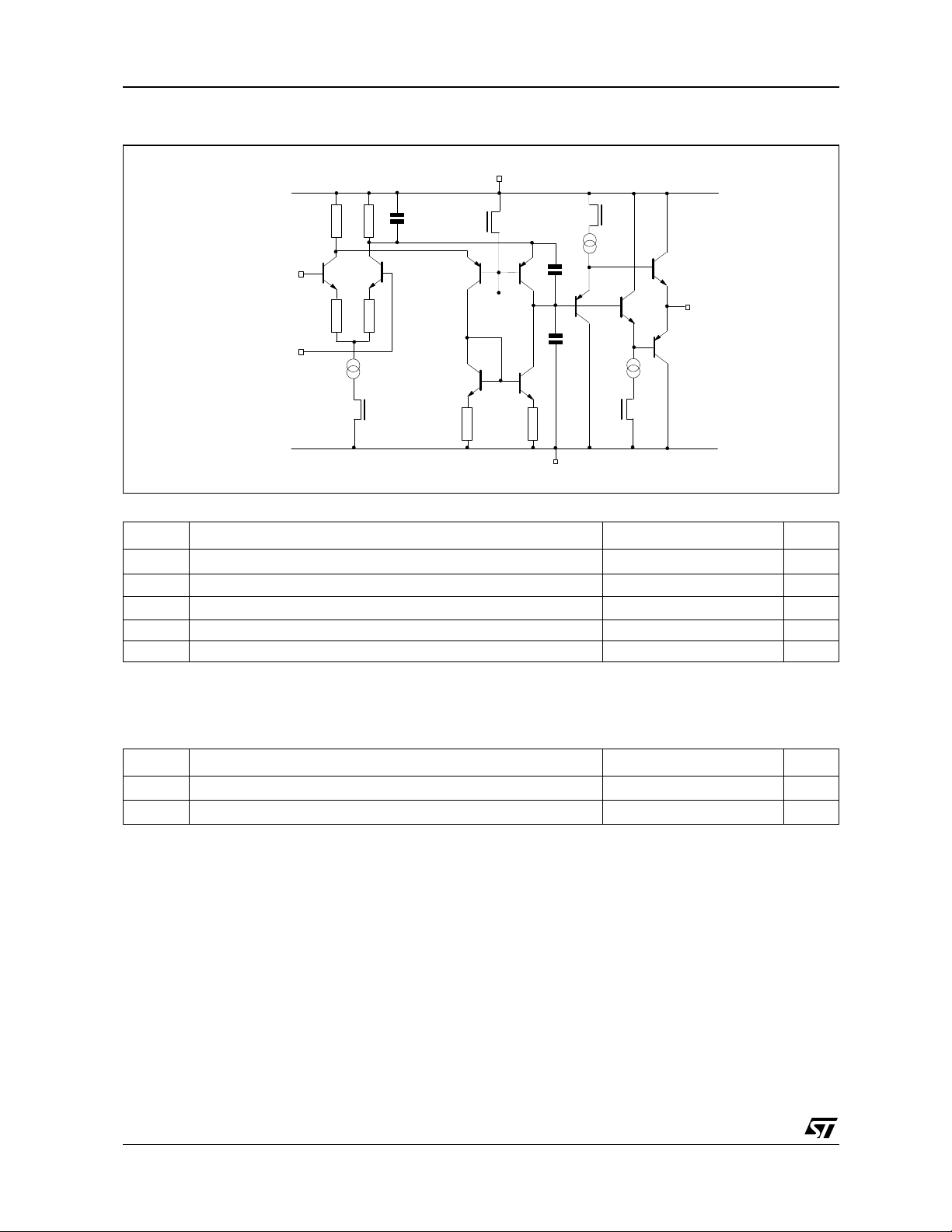
SCHEMATIC DIAGRAM
+
V
CC
stdby
output
C
c
stdby
-
non inverting
input
inverting
input
stdby
stdby
Internal
V
ref
V
CC
MAXIMUM RATINGS
Symbol Parameter Value Unit
V
T
T
Supply Voltage
CC
V
Differential Input Voltage
id
V
i Input Voltage
Operating Free-Air Temperature range -40 to +125 °C
oper
Storage Temperature Range -65 to +150 °C
stg
1)
2)
3)
1. All voltages values, except differential voltage are with respect to network ground terminal
2. Dif ferential voltages are the non-inver ting input ter minal with respect to the inv erting input terminal
3. The magnitude of input and out put voltages m ust never exc eed V
CC
+
+0.3V
14 V
±5 V
-0.3 to 12 V
OPERATING CONDITIONS
Symbol Parameter Value Unit
V
2/11
Supply Voltage 7 to 12 V
CC
V
Common Mode Input Voltage Range
ic
V
CC
-
+2 to V
CC
+
-1
V
ELECTRICAL CHARACTERISTICS
V
CC
+
= 5V, V
-
= -5V, pin 8 connected to 0V, pin 9 connected to V
CC
CC
+
, T
= 25°C
amb
(unless otherwise specified)
Symbol Parameter Min. Typ. Max. Unit
V
io
I
io
I
ib
I
CC
CMR
SVR
Avd
V
OH
V
OL
I
o
GBP
f
T
SR
e
n
m
φ
V
O1/VO2
Gf
THD
G
∆
∆ϕ
Input Offset Voltage Vic = Vo = 0V
T
. ≤ T
. ≤ T
. ≤ T
. ≤ T
. ≤ T
. ≤ T
. ≤ T
amb
amb
amb
amb
amb
amb
amb
≤ T
≤ T
.
≤ T
≤ T
≤ T
≤ T
≤ T
max.
max.
max.
max.
max.
max
max.
= -3V to +4V, Vo = 0V
ic
= ±5V to ±3V
CC
= 10k
L
Vo = ±2.5V
Ω,
80
70
60
50
57
54
12
515
4.5 6
100
75
70
min
Input Offset Current
T
min
Input Bias Current
T
min
Supply Current (per amplifier, no load)
T
min
Common-mode Rejection Ratio V
T
min
Supply Voltage Rejection Ratio V
T
min
Large Signal Voltage Gain R
T
min
High Level Output Voltage Vid = 1V
= 600
R
R
. ≤ T
T
min
amb
≤ T
max.
RL = 150Ω
L
= 150
L
Ω
Ω
3
2.5
3.5
3
2.4
Low Level Output Voltage Vid = 11V
= 600
R
R
. ≤ T
T
min
amb
≤ T
max.
RL = 150Ω
L
= 150
L
Ω
Ω
-3.5
-2.8
Output Short Circuit Current Vid = ±1V
Source
Sink
. ≤ T
T
min
amb
≤ T
max.
Source
Sink
20
20
15
15
36
40 mA
Gain Bandwidth Product
= 100, RL = 600Ω, CL = 15pF, f = 7.5MHz
A
VCL
90 150
Transition Frequency 90 MHz
Slew Rate
V
= -2 to +2V, A
in
Equivalent Input Voltage Noise Rs = 50Ω, f = 1kHz
Phase Margin A
VM
= +1
= +1, RL = 600
VCL
CL = 15pF
Ω,
70 110
4.2 nV/√Hz
35 Degrees
Channel Seperation f = 1MHz to 10MHz 65 dB
Gain Flatness f = DC to 6MHz, A
Total Harmonic Distortion f = 1kHz, V
Differential Gain f = 3.58MHz, A
Differential Phase f = 3.58MHz, A
= 10dB
VCL
= ±2.5V, RL = 600
o
= +2, RL = 150
VCL
= +2, RL = 150
VCL
Ω
Ω
Ω
0.01 %
0.03 %
0.07 Degree
3
5
5
20
8
-3
-2.5
-2.4
0.1 dB
TSH94
mV
A
µ
A
µ
mA
dB
dB
dB
V
V
MHz
V/µs
3/11
TSH94
STANDBY MODE V
+
= 5V, V
CC
-
= -5V, T
CC
= 25°C (unless otherwise specified)
amb
Symbol Parameter Min. Typ. Max. Unit
V
Pin 8/9 Threshold Voltage for STANDBY Mode
SBY
+
V
CC
-2.2 V
+
-1.6 V
CC
CC
+
-1.0
Total Consumption
I
CC SBY
I
sol
t
ON
t
OFF
I
D
I
OL
I
IL
Standby 1 & 2 = 0
Standby 1 & 2 = 1
Standby 1 = 1, Standby 2 = 0
Input/Output Isolation (f = 1MHz to 10MHz) 70 dB
Time from Standby Mode to Active Mode 200 ns
Time from Active Mode to Standby Mode 200 ns
Standby Driving Current 2 pA
Output Leakage Current 20 pA
Input Leakage Current 20 pA
13.7
13.7
9.4
LOGIC INPUT STATUS
Standby 1 Standby 2 Op-Omp 2 Op-Amp 3 Op-Amp 1 & 4
0 0 Enable Standby Enable
0 1 Enable Enable Enable
1 0 Standby Standby Enable
1 1 Standby Enable Enable
STANDBY POSITION
STANDBY MODE
V
mA
V
CC
V
CC
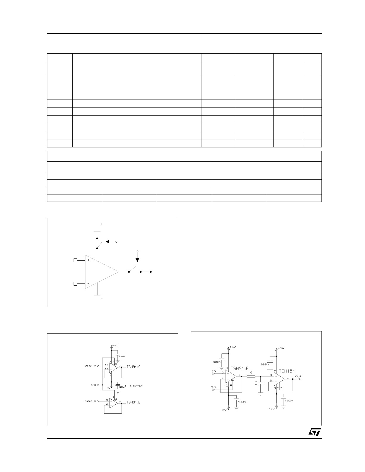
APPLICATIONS
SIGNAL MULTIPLEXING
standby
To put the device in standby, just apply a logic
level on the standby MOS input. As ground is a virtual level for the device, threshold voltage has
been refered to V
CC
+
at V
+
- 1.6V typ.
CC
In standby m ode, the output goes in hi gh impedance in 200ns. Be aware that all maximum rating
must still be followed in this mode. It leads to
swing limitation while using the device in signal
multiplexing configuration with followers, differential input voltage mu st not exceed ±5V limit ing input swing to 2.5Vpp.
SAM PLE AND HOLD
4/11

APPLICATIONS
VIDEO LINE TRANSCEIVER WITH REMOTE CONTROL
TSH94
PRINTED CIRCUIT LAYOUT
As for any high frequency device, a few rules must
be observed when designing the PCB to get the
best performances from this high speed op amp.
From the most to the least important points :
❑ Each power supply lead has to be
by-passed to ground with a 10nF ceramic
capacitor very close to the device and
10µF capacitor.
❑ To provide low inductance and low resist-
ance common return, us e a ground plane
or common point return for power and signal.
❑ All leads must be wide and as short as pos-
sible especially for op amp inputs. This is in
order to decrease parasitic capacitance
and inductance.
❑ Use small resistor values to decrease time
constant with parasitic capacitance.
❑ Choose component sizes as s mall as pos -
sible (SMD).
❑ On output, decrease capacitor load so as
to avoid circuit stability being degraded
which may cause oscillation. You can also
add a serial resistor in order to minimise its
influence.
5/11

TSH94
INPUT OFFSET VOLTAGE DRIFT VERSUS
TEMPERATURE
LARGE SIGNAL FOLLOWER RESPONSE
STATIC OPEN LOOP VOLTAGE GAIN
SMALL SIGNAL FOLLOWER RESPO N SE
OPEN LOOP FREQUENCY RESPONSE AND
PHASE SHIFT
6/11
CLOSE LOOP FREQUENCY RESPONSE

TSH94
AUDIO BANDWIDTH FREQUENCY
RESPONSE AND PHASE SHIFT
(TSH94 vs Standard 15MHz Audio Op-Amp)
CROSS TALK ISOLATION VERSUS
FREQUENCY (SO16 PACKAGE)
GAIN FLATNESS AND PHASE SHIF T VERSUS
FREQUENCY
CROSS TALK ISOLATION VERSUS
FREQUENCY (SO16 PACKAGE)
INPUT/OUTPUT ISOLATION IN STA NDBY
MODE (SO16 PACKAGE)
STANDBY SWITCHING
7/11

TSH94
SIGNAL MULTIPLEXING (cf p. 5/10)
DIFFERENTIAL INPUT IMPEDANCE VERSUS
FREQUENCY
120
100
80
)
W
60
Zin-com (M
40
COMMON INPUT IMPEDANCE VERSUS
FREQUENCY
4.5
4.0
3.5
3.0
)
W
2.5
2.0
Zin-diff (k
1.5
1.0
0.5
1k 10k 100k 1M 10M 100M
Frequency (Hz)
20
1k 10k 100k 1M 10M 100M
Frequency (Hz)
8/11

MACROMODEL
Applies to: TSH94I (model without standby)
TSH94
** Standard Linear Ics Macromodels, 1996.
** CONNECTIONS :
* 1 INVERTING INPUT
* 2 NON-INVERTING INPUT
* 3 OUTPUT
* 4 POSITIVE POWER SUPPLY
* 5 NEGATIVE POWER SUPPLY
.SUBCKT TSH94 1 3 2 4 5 (analog)
*********** *********************************************
.MODEL MDTH D IS=1E-8 KF =1.809064E-15
CJO=10F
* INPUT STAGE
CIP 2 5 1.000000E-12
CIN 1 5 1.000000E-12
EIP 10 5 2 5 1
EIN 16 5 1 5 1
RIP 10 11 2.600000E-01
RIN 15 16 2.600000E-01
RIS 11 15 3.645298E-01
DIP 11 12 MDTH 400E-12
DIN 15 14 MDTH 400E-12
VOFP 12 13 DC 0.000000E+00
VOFN 1314DC 0
IPOL 13 5 1.000000E-03
CPS 11 15 2.986990E-10
DINN 17 13 MDTH 400E-12
VIN 17 5 2.000000e+00
DINR 15 18 MDTH 400E-12
VIP 4 18 1.000000E+00
FCP 4 5 VOFP 3.500000E+0 0
FCN 5 4 VOFN 3.500000E+00
FIBP 2 5 VOFP 1.000000E-02
FIBN 5 1 VOFN 1.000000E-02
* AMPLIFYING STAG E
FIP 5 19 VOFP 2.530000E+02
FIN 5 19 VOFN 2.530000E+02
RG1 19 5 3.160721E+03
RG2 19 4 3.160721E+03
CC 19 5 2.00000E-09
DOPM 19 22 MDTH 400E-12
DONM 21 19 MDTH 400E-12
HOPM 22 28 VOUT 1.504000E+03
VIPM 28 4 5.000000E+01
HONM 21 27 VOUT 1.400000E+03
VINM 5 27 5.000000E+01
*********** ************
RZP1 5 80 1E+06
RZP2 4 80 1E+06
GZP 5 82 19 80 2.5E-05
RZP2H 83 4 10000
RZP1H 83 82 80000
RZP2B 84 5 10000
RZP1B 82 84 80000
LZPH 4 83 3.535e-02
LZPB 84 5 3.535e-02
EOUT 26 23 82 5 1
VOUT 23 5 0
ROUT 26 3 35
COUT 3 5 30.000000E-12
DOP 19 25 MDTH 400E-12
VOP 4 25 2.361965E+00
DON 24 19 MDTH 400E-12
VON 24 5 2.361965E+00
.ENDS
ELECTRICAL CHARACTERISTICS
= ±5V, T
V
CC
Symbol Conditions Value Unit
V
io
A
vd
I
CC
V
icm
V
OH
V
OL
I
sink
I
sourceVo
GBP
SR
m
φ
= 25°C (unless otherwise specificed)
amb
0mV
RL = 600
No load / Ampli 5.2 mA
RL = 600
RL = 600
Vo = 0V
R
R
R
Ω
Ω
Ω
= 0V
= 600Ω, CL = 15pF
L
= 600Ω, CL = 15pF
L
= 600Ω, CL = 15pF
L
3.2 V/mV
-3 to 4 V
+3.6 V
-3.6 V
40 mA
40 mA
147 MHz
110 V/µs
42 Degrees
9/11

TSH94
Applies to: TSH94I (model with standby)
* 1 INVERTING INPUT
* 2 NON-INVERTING INPUT
* 3 OUTPUT
* 4 POSITIVE POWER SUPPLY
* 5 NEGATIVE POWER SUPPLY
* 6 STANDBY
.SUBCKT TSH94 1 3 2 4 5 6 (analog)
********************************************************
**************** switch *******************
.SUBCKT SWITCH20 10 IN OUT COM
.MODEL DIDEAL D N=0.1 IS=1E-08
DP IN 1 DIDEAL 400E-12
DN OUT 2 DIDEAL 400E-12
EP 1 OUT COM 10 2
EN 2 IN COM 10 2
RFUIT1 IN 1 1E+09
RFUIT2 OUT 2 1E+09
RCOM COM 0 1E+12
.ENDS SWITCH
**************** inverter *****************
.SUBCKT INV 20 10 IN OUT
.MODEL DIDEAL D N=0.1 IS=1E-08
RP1 20 15 1E+09
RN1 15 10 1E+09
RIN IN 10 1E+12
RIP IN 20 1E+12
DPINV OUT 20 DIDEAL 400E-12
DNINV 10 OUT DIDEAL 400E-12
GINV 0 OUT IN 15 -6.7E-7
CINV 0 OUT 210f
.ENDS INV
***************** AOP **********************
.MODEL MDTH D IS=1E-8 KF =1.809064E-15
CJO=10F
* INPUT STAGE
CIP 2 5 1.000000E-12
CIN 1 5 1.000000E-12
EIP 10 5 2 5 1
EIN 16 5 1 5 1
RIP 10 11 2.600000E-01
RIN 15 16 2.600000E-01
RIS 11 15 3.645298E-01
DIP 11 12 MDTH 400E-12
DIN 15 14 MDTH 400E-12
VOFP 12 13 DC 0.000000E+00
VOFN 1314DC 0
FPOL 13 5 VSTB 1E+03
CPS 11 15 2.986990E-10
DINN 17 13 MDTH 400E-12
VIN 17 5 2.000000e+00
DINR 15 18 MDTH 400E-12
VIP 4 18 1.000000E+00
FCP 4 5 VOFP 3.500000E+0 0
FCN 5 4 VOFN 3.500000E+00
ISTB0 4 5 130UA
FIBP 2 5 VOFP 1.000000E-02
FIBN 5 1 VOFN 1.000000E-02
* AMPLIFYING STAG E
FIP 5 19 VOFP 2.530000E+02
FIN 5 19 VOFN 2.530000E+02
RG1 19 120 3.160721E+03
XCOM1 4 0 120 5 COM SWITCH
RG2 19 121 3.160721E+03
XCOM2 4 0 4 121 COM SWITCH
CC 19 5 2.00000E-09
DOPM 19 22 MDTH 400E-12
DONM 21 19 MDTH 400E-12
HOPM 22 28 VOUT 1.504000E+03
VIPM 28 4 5.000000E+01
HONM 21 27 VOUT 1.400000E+03
VINM 5 27 5.000000E+01
*********** ZP **********
RZP1 5 80 1E+06
RZP2 4 80 1E+06
GZP 5 82 19 80 2.5E-05
RZP2H 83 4 10000
RZP1H 83 82 80000
RZP2B 84 5 10000
RZP1B 82 84 80000
LZPH 4 83 3.535e-02
LZPB 84 5 3.535e-02
*********** ***************
EOUT 26 23 82 5 1
VOUT 23 5 0
ROUT 26 103 35
COUT 103 5 30.000000E-12
XCOM 4 0 103 3 COM SWITCH
DOP 19 25 MDTH 400E-12
VOP 4 25 2.361965E+00
DON 24 19 MDTH 400E-12
VON 24 5 2.361965E+00
********** STA N D BY **** ****
RMI1 4 111 1E+7
RMI2 0 111 2E+7
RONOFF 6 60 1K
CONOGG 60 0 10p
RSTBIN 60 0 1E+12
ESTBIN 106 0 6 0 1
ESTBREF 106 107 111 0 1
DSTB1 107 108 MDTH 400E-12
VSTB 108 109 0
ISTB 109 0 1U
RSTB 109 110 1
DSTB2 0 110 MDTH 400E-12
XINV 4 0 6 COM INV
.ENDS
10/11

PACKAGE MECHANICAL DATA
16 PINS - PLASTIC MICROPACKAGE (SO)
TSH94
Dim.
Millimeters Inches
Min. Typ. Max. Min. Typ. Max.
A 1.75 0.069
a1 0.1 0.2 0.004 0.008
a2 1.6 0.063
b 0.35 0.46 0.014 0.018
b1 0.19 0.25 0.007 0.010
C 0.5 0.020
c1 45° (typ.)
D 9.8 10 0.386 0.394
E 5.8 6.2 0.228 0.244
e 1.27 0.050
e3 8.89 0.350
F 3.8 4.0 0.150 0.157
G 4.6 5.3 0.181 0.209
L 0.5 1.27 0.020 0.050
M 0.62 0.024
S 8° (max.)
Inform ation f urnished is beli eved to b e accu rate an d reliab le. Howe ver, ST Micro electro nics ass umes no respo nsibility for th e
consequences of use of such information nor f or a ny infringement of patent s or other ri ghts of t hird parti es which ma y result
from its use. No license is granted by implication or otherwise under any patent or patent rights of STMicroelectronics.
Specifications mentioned in this publication are subject to change witho ut notic e. This public ation sup ersedes and rep laces all
information previously supplied. STMicroelectroni cs products are not authorized for use as critical components in life support
devices or systems without express written approval of STMicroelectronics.
© The ST logo is a registered trademark of STMicroelectronics
© 2000 STM icroelectronics - Printed in Ital y - All Right s Reserved
STMicroelectronics GROUP OF COMPANIES
Austra lia - Brazil - Chi na - Finland - F rance - Germ any - Hong Kong - India - Italy - Japan - Mal aysia - Malt a - M orocco
Singap ore - Spain - Sweden - Switzerland - Uni ted Kingdom
© htt p://w ww.st.com
11/11
 Loading...