

SGS Thomson Microelectronics TSH94IN, TSH94ID, TSH94 Datasheet
TSH94
HIGH SPEED LOW POWERQUAD
OPERATIONALAMPLIFIER (WITH STANDBY POSITION)
November 1998
.
2 SEPARATE STANDBY : REDUCED
CONSUMPTION AND HIGH IMPEDANCE
OUTPUTS
.
LOW SUPPLYCURRENT : 4.5mA/amp.typ.
.
HIGHSPEED: 150MHz - 110V/µs
.
UNITYGAINSTABILITY
.
LOW OFFSETVOLTAGE: 3mV
.
LOW NOISE 4.2 nV/√Hz
.
LOW COST
.
SPECIFIEDFOR 600Ω AND 150Ω LOADS
.
HIGHVIDEOPERFORMANCES :
DifferentialGain : 0.03%
DifferentialPhase : 0.07
o
Gain Flatness : 6MHz, 0.1dB max. @ 10dB
gain
.
HIGHAUDIO PERFORMANCES
Non-inve rting Input 2
Non-inve rting Input 1
-
CCV
1
2
3
4
5
6
7
12
13
14
15
16
CC
V
+
Output 3
Output 4
Non-inve rting Input 4
Inverting Input 4
Non-inve rting Input 3
Inverting Input 3
-
+
-
+
-
+
-
+
Inverting Input 1
Output 2
9
8
Standby 1
11
10
Standby2
Output 1
Inverting Input 2
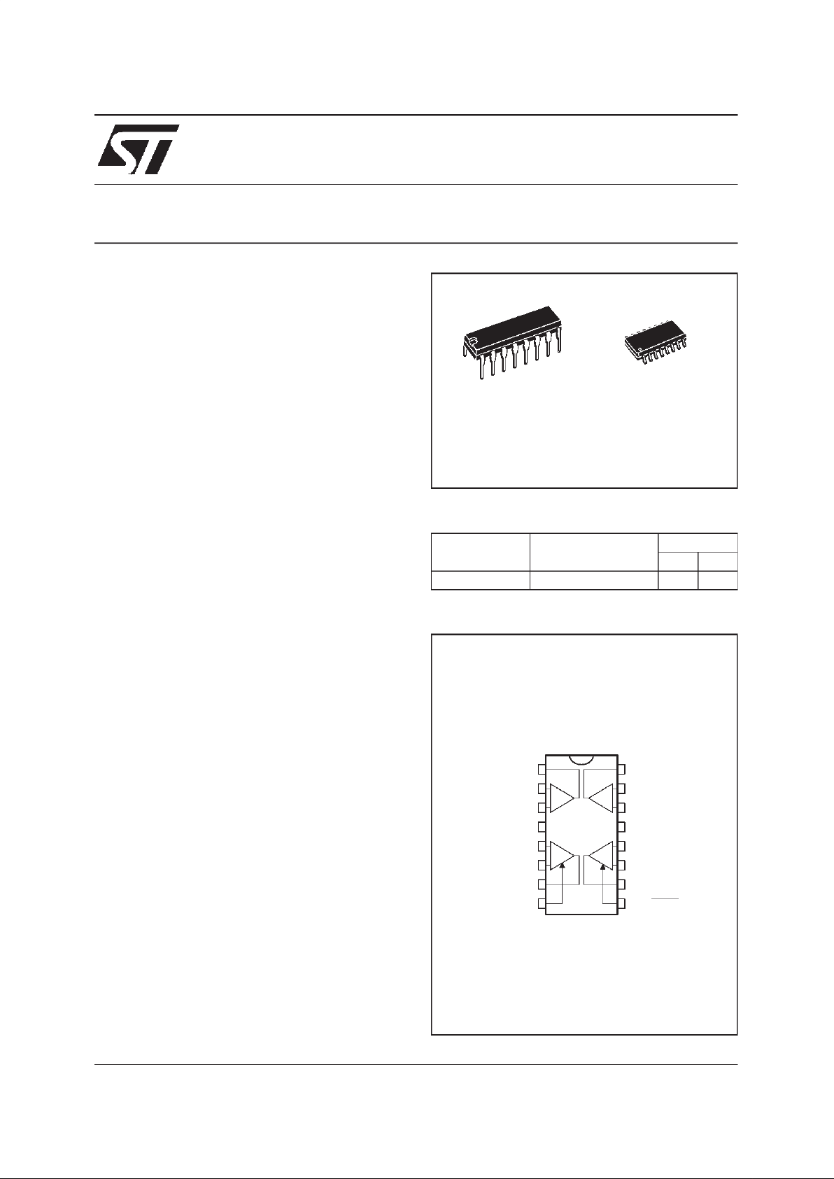
PIN CONNECTIONS (top view)
N
DIP16
(Plastic Package)
DESCRIPTION
The TSH94 is a quad low power high frequency
op-amp, designated for high quality video signal
processing. The device offers an excellent speed
consumption ratio with 4.5mA/amp. for 150MHz
bandwidth.
High slew rate and low noise make it also suitable
for high quality audio applications.
The TSH94 offers 2 separate complementary
STANDBY pins :
• STANDBY1 acting on the n°2 operator
• STANDBY2 acting on the n°3 operator
Theyreducetheconsumptionofthecorresponding
operator and put the output in a high impedance
state.
D
SO16
(Plastic Micropackage)
ORDER CODES
Part Number Temperature Range
Package
ND
TSH94I -40, +125
o
C ••
1/12
ABSOLUTE MAXIMUMRATINGS
Symbol Parameter Value Unit
V
CC
Supply Voltage -(note 1) 14 V
V
id
Differential Input Voltage - (note 2) ±5V V
V
i
InputVoltage - (note 3) -0.3 to 12 V
T
oper
Operating Free Air Temperature Range -40 to +125
o
C
T
stg
StorageTemperature -65 to +150
o
C
Notes : 1. All voltage values, except differential voltage are with respect to network ground terminal.
2. Differential voltagesare the non-inverting input terminal with respect tothe inverting input terminal.
3. The magnitude of input and output voltages must never exceed V
CC
+
+0.3V.
OPERATING CONDITIONS
Symbol Parameter Value Unit
V
CC
Supply Voltage 7 to 12 V
V
icm
Common ModeInput Voltage Range V
CC
-
+2V to V
CC
+
-1 V
non inverting
input
inverting
input
V
CC
+
C
c
output
V
CC
-
V
Internal
ref
stdby
stdby
stdby
stdby
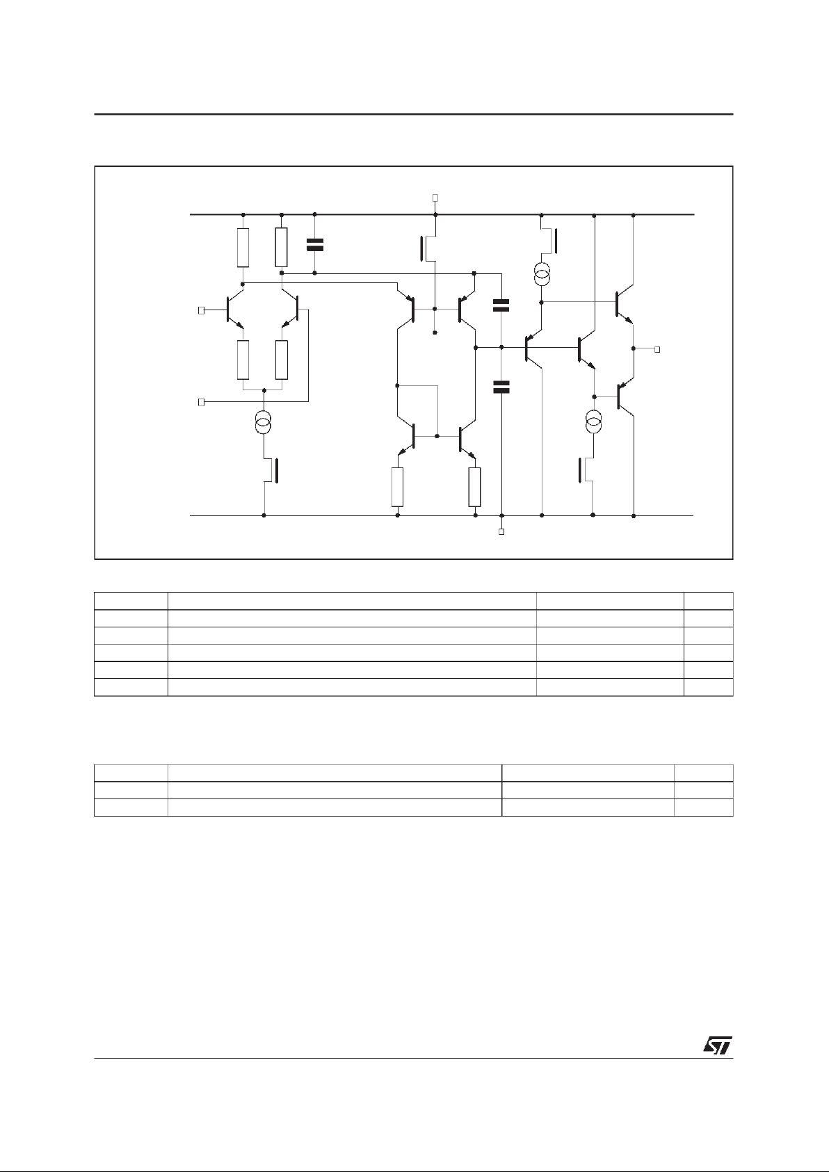
SCHEMATIC DIAGRAM
TSH94
2/12
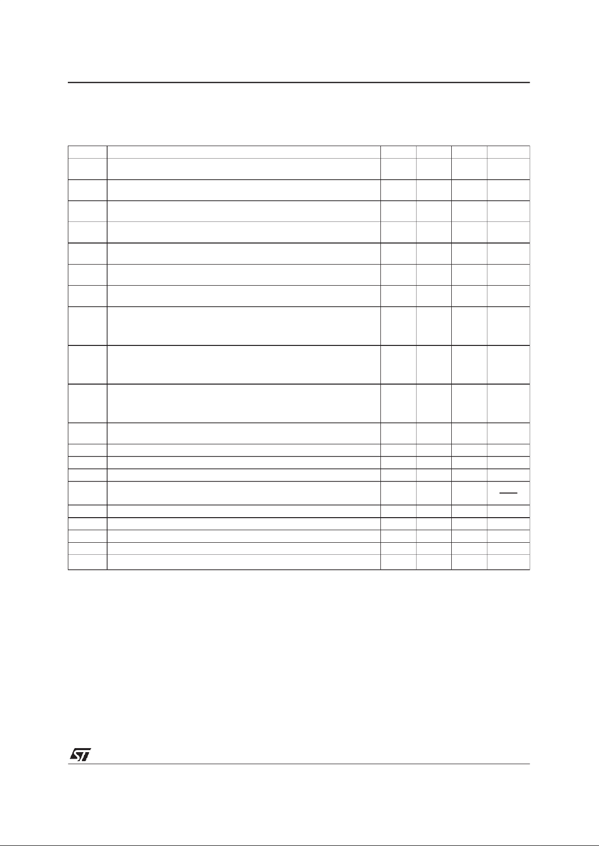
ELECTRICAL CHARACTERISTICS
V
CC
+
=5V,V
CC
-
=-5V, pin 8 connectedto 0V,pin 9 connectedto V
CC
+
,T
amb
=25oC
(unless otherwisespecified)
Symbol Parameter Min. Typ. Max. Unit
V
io
Input Offset Voltage (Vic=Vo= 0V)
T
min.
≤ T
amb.
≤ T
max.
3
5
mV
I
io
Input Offset Current
T
min.
≤ T
amb.
≤ T
max.
12
5
µA
I
ib
Input Bias Current
T
min.
≤ T
amb.
≤ T
max.
51520µA
I
CC
Supply Current (per amplifier, no load)
T
min.
≤ T
amb.
≤ T
max.
4.5 6
8
mA
CMR Common Mode Rejection Ratio (V
ic
= -3V to +4V, Vo= 0V)
T
min.
≤ T
amb.
≤ T
max.
80
70
100 dB
SVR Supply Voltage Rejection Ratio (V
CC
= ±5V to ±3V)
T
min.
≤ T
amb.
≤ T
max.
60
50
75 dB
A
vd
Large Signal Voltage Gain (RL=10kΩ,VO=±2.5V)
T
min.
≤ T
amb.
≤ T
max.
57
54
70 dB
V
OH
High Level Output Voltage (Vid= 1V)
R
L
= 600Ω
R
L
= 150Ω
T
min.
≤ T
amb.
≤ T
max.
RL= 150Ω
3
2.5
2.4
3.5
3
V
V
OL
Low Level Output Voltage (Vid= -1V)
R
L
= 600Ω
R
L
= 150Ω
T
min.
≤ T
amb.
≤ T
max.
RL= 150Ω
-3.5
-2.8
-3
-2.5
-2.4
V
I
o
Output Short Circuit Current (Vid= ±1V) Source
Sink
T
min.
≤ T
amb.
≤ T
max.
Source
Sink
20
20
15
15
36
40
mA
GBP Gain Bandwidth Product
(A
VCL
= 100, RL= 600Ω,CL= 15pF, f =7.5MHz) 90 150
MHz
f
T
Transition Frequency 90 MHz
SR Slew Rate (A
VCL
= +1, RL= 600Ω,CL= 15pF, Vin= -2 to +2V) 70 110 V/µs
∅m Phase Margin (A
VM
= +1) 35 Degrees
e
n
Equivalent Input Noise Voltage (Rs=50Ω, f = 1kHz) 4.2
nV
√Hz
V
O1/VO2
Channel Separation (f = 1MHz to 10MHz) 65 dB
Gf Gain Flatness (f = DC to 6MHz, A
VCL
= 10dB) 0.1 dB
THD Total Harmonic Distortion (f = 1kHz, V
o
= ±2.5V, RL= 600Ω) 0.01 %
∆G Differential Gain (f = 3.58MHz, A
VCL
= +2, RL= 150Ω) 0.03 %
∆
ϕ
DifferentialPhase (f = 3.58MHz, A
VCL
= +2, RL= 150Ω)
0.07 Degree
TSH94
3/12
LOGIC INPUT STATUS
Standby 1 Standby 2 Op-amp 2 Op-amp 3 Op-amp 1 & 4
0 0 Enable Standby Enable
0 1 Enable Enable Enable
1 0 Standby Standby Enable
1 1 Standby Enable Enable
STANDBY MODE V
CC
+
=5V,V
CC
-
=-5V, T
amb
=25oC (unless otherwisespecified)
Symbol Parameter Min. Typ. Max. Unit
V
SBY
Pin 8/9 Threshold Voltage for STANDBY Mode VCC+-2.2 V
CC
+
-1.6 V
CC
+
-1.0 V
I
CC SBY
Total Consumption
Standby 1 & 2 = 0
Standby 1 & 2 = 1
Standby 1 = 1, Standby 2 = 0
13.7
13.7
9.4
mA
I
sol
Input/Output Isolation (f = 1MHz to 10MHz) 70 dB
t
ON
Time from Standby Mode to Active Mode 200 ns
t
OFF
Time from Active Mode to Standby Mode 200 ns
I
D
Standby Driving Current 2 pA
I
OL
Output Leakage Current 20 pA
I
IL
Input Leakage Current 20 pA
V
CC
V
CC
sta ndby
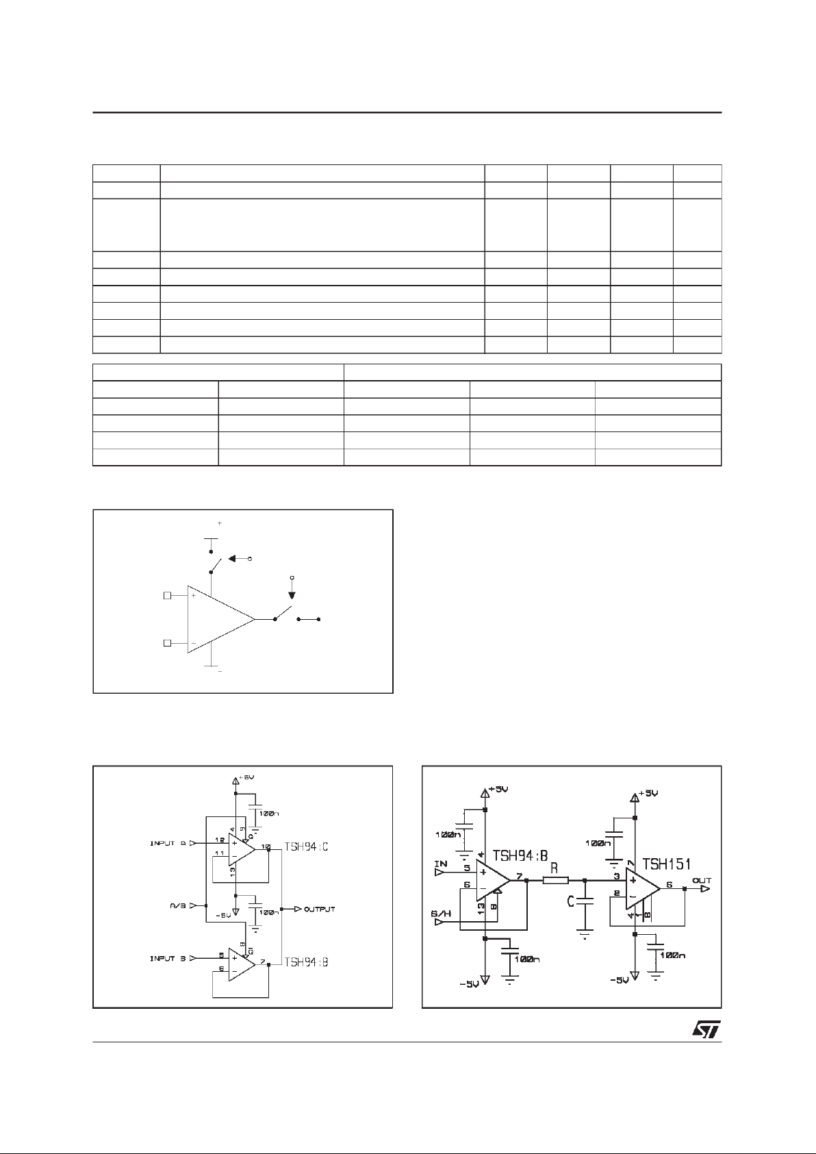
STANDBY POSITION
To put thedevicein standby, just applya logiclevel
on the standby MOS input. As ground is a virtual
level for the device, threshold voltage has been
referedto V
CC
+
at V
CC
+
- 1.6V typ.
In standby mode, the output goes in high impedance in 200ns. Be aware that all maximum rating
muststillbe followedin thismode. It leadsto swing
limitationwhile usingthe deviceinsignal multiplexing configuration with followers, differential input
voltage must not exceed ±5V limiting input swing
to 2.5Vpp.
STANDBY MODE
APPLICATIONS
SIGNAL MULTIPLEXING SAMPLEAND HOLD
TSH94
4/12
 Loading...