

.
LOW SUPPLYCURRENT:4.5mA/amp.typ.
.
HIGHSPEED : 150MHz- 110V/µs
.
UNITYGAIN STABILITY
.
LOW OFFSETVOLTAGE: 4mV
.
LOW NOISE 4.2 nV/√Hz
.
LOW COST
.
SPECIFIEDFOR 600Ω AND 150Ω LOADS
.
HIGHVIDEO PERFORMANCES :
Differential Gain : 0.03%
DifferentialPhase : 0.07
Gain Flatness : 6MHz, 0.1dBmax. @ 10dB
gain
.
HIGHAUDIO PERFORMANCES
.
ESD TOLERANCE: 2kV
.
SPICEMACROMODEL INCLUDED IN THIS
SPECIFICATION
o
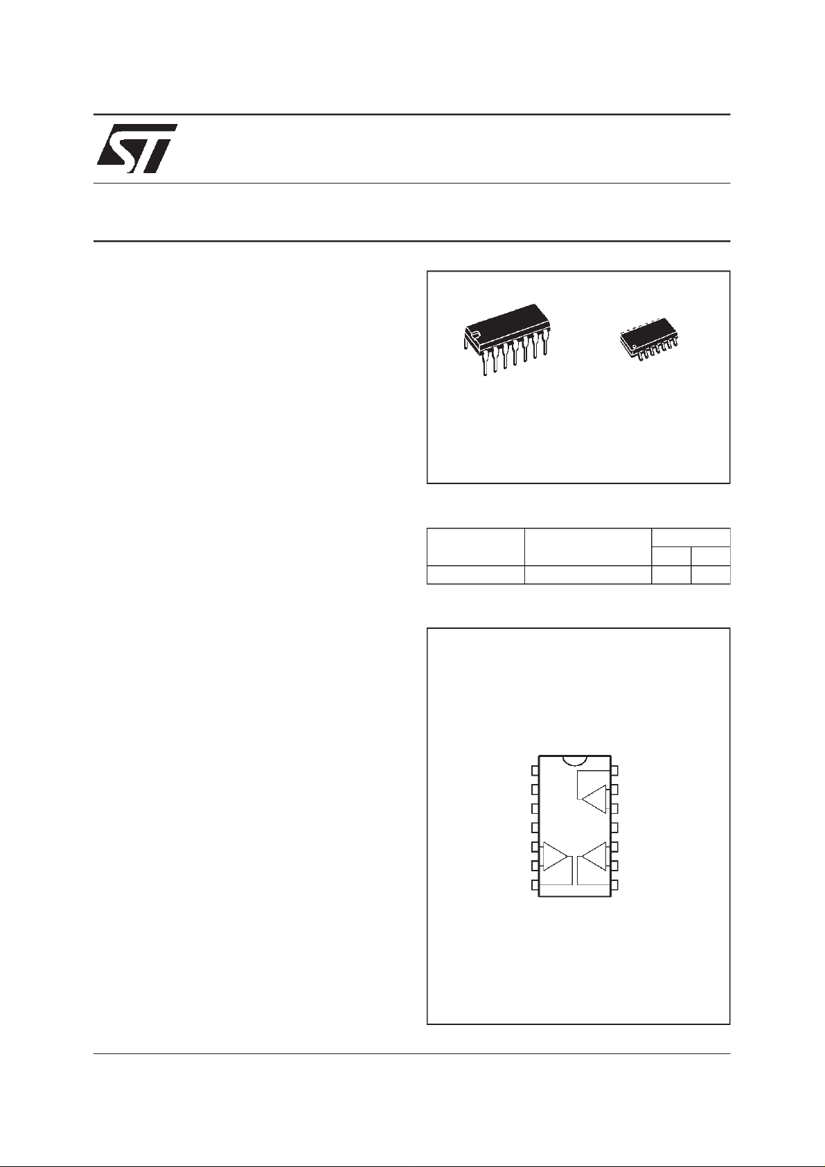
TSH93
HIGH SPEED LOW POWER TRIPLE
OPERATIONALAMPLIFIER
N
DIP14
(Plastic Package)
ORDER CODES
Part Number Temperature Range
TSH93I -40, +125
(Plastic Micropackage)
D
SO14
Package
o
C ••
ND
DESCRIPTION
The TSH93 is a triple low power high frequency
op-amp, designated for high quality video signal
processing. The device offers an excellentspeed
consumption ratio with 4.5mA/amp. for 150MHz
bandwidth.
High slewrate and low noisemake it also suitable
for high quality audio applications.
PIN CONNECTIONS (top view)
N.C.
1
2
N.C.
N.C.
V
CC
Non-inve rting Input 1
Inverting Input 1
Output 1
3
+
4
5
+
-
6
7
-
+
+
-
14
Output 3
Inverting Input 3
13
12
Non-inverting Input 3
-
CCV
11
10
Non-inverting Input 2
Inverting Input 2
9
Output 2
8
November 1998
1/9

TSH93
SCHEMATIC DIAGRAM (1/3)
non inverting
input
+
V
CC
inverting
input
Internal
V
ref
C
c
-
V
CC
output
ABSOLUTE MAXIMUMRATINGS
Symbol Parameter Value Unit
V
CC
V
id
V
T
oper
T
stg
Notes : 1. All voltage values, except differential voltage are with respect to network ground terminal.
Supply Voltage - (note 1) 14 V
Differential Input Voltage - (note 2) ±5V V
Input Voltage - (note 3) -0.3 to 12 V
i
Operating Free Air Temperature Range -40 to +125
Storage Temperature -65 to +150
2. Differential voltagesare the non-inverting input terminal with respect to the inverting input terminal.
3. The magnitude of inputand output voltages must never exceed V
CC
+
+0.3V.
OPERATING CONDITIONS
Symbol Parameter Value Unit
V
CC
V
icm
Supply Voltage 7 to 12 V
Common Mode Input Voltage Range V
CC
-
+2V to V
+
-1 V
CC
o
C
o
C
2/9
TSH93
ELECTRICAL CHARACTERISTICS
+
=5V,V
V
CC
Symbol Parameter Min. Typ. Max. Unit
V
io
I
io
I
ib
I
CC
CMR Common Mode Rejection Ratio (V
SVR Supply Voltage Rejection Ratio (V
A
vd
V
OH
V
OL
I
o
GBP Gain Bandwidth Product
f
T
SR Slew Rate (A
∅m Phase Margin (A
e
n
V
O1/VO2
Gf Gain Flatness (f= DC to6MHz, A
THD Total Harmonic Distortion (f = 1kHz, V
∆G Differential Gain (f = 3.58MHz, A
∆
ϕ
-
=-5V, T
CC
Input Offset Voltage(Vic=Vo= 0V)
≤ T
T
min.
amb.
Input Offset Current
≤ T
T
min.
amb.
Input Bias Current
≤ T
T
min.
amb.
Supply Current (per amplifier, no load)
≤ T
T
min.
amb.
≤ T
T
min.
amb.
≤ T
T
min.
amb.
Large Signal Voltage Gain (RL= 10kΩ,VO=±2.5V)
≤ T
T
min.
amb.
=25oC (unlessotherwise specified)
amb
≤ T
max.
≤ T
max.
≤ T
max.
≤ T
max.
= -3V to +4V,Vo= 0V)
≤ T
≤ T
≤ T
max.
max.
max.
ic
= ±5V to ±3V)
CC
80
70
60
50
57
54
4
mV
6
12
µA
5
51520µA
4.5 6
mA
8
100 dB
75 dB
70 dB
High Level Output Voltage (Vid= 1V)
= 600Ω
R
L
= 150Ω
R
≤ T
T
min.
amb.
≤ T
max.
L
RL= 150Ω
3
2.5
2.4
3.5
3
Low Level Output Voltage (Vid= -1V)
= 600Ω
R
L
= 150Ω
R
≤ T
T
min.
amb.
≤ T
max.
L
RL= 150Ω
Output Short CircuitCurrent (Vid= ±1V) Source
Sink
≤ T
T
min.
amb.
≤ T
max.
Source
Sink
20
20
15
15
-3.5
-2.8
36
40
-3
-2.5
-2.4
mA
MHz
= 100, RL= 600Ω,CL= 15pF, f =7.5MHz) 90 150
(A
VCL
Transition Frequency 90 MHz
= +1, RL= 600Ω,CL= 15pF, Vin= -2 to +2V) 62 110 V/µs
VCL
= +1) 35 Degrees
VM
Equivalent Input Noise Voltage (Rs=50Ω, f = 1kHz) 4.2
nV
√Hz
Channel Separation (f = 1MHz to 10MHz) 65 dB
= 10dB) 0.1 dB
VCL
= ±2.5V, RL= 600Ω) 0.01 %
o
= +2, RL= 150Ω) 0.03 %
VCL
DifferentialPhase (f = 3.58MHz, A
= +2, RL= 150Ω)
VCL
0.07 Degree
V
V
3/9

TSH93
PRINTEDCIRCUIT LAYOUT
As for any highfrequencydevice,a fewrules must
be observed when designing the PCB to get the
best performancesfrom this high speed op amp.
From the mostto the least important points :
•
Each power supply lead has to be by-passedto
ground with a 10nF ceramic capacitor very
close to the device and 10µF capacitor.
•
To provide low inductance and low resistance
common return, use a ground plane or common
point return for power and signal.
INPUT OFFSET VOLTAGE DRIFT VERSUS
TEMPERATURE
•
All leads must be wide and as short as possible
especially for op amp inputs. This is in order to
decreaseparasitic capacitance and inductance.
•
Use small resistor values to decrease time constant withparasitic capacitance.
•
Choose component sizes as small as possible
(SMD).
•
On output, decrease capacitor load so as to
avoid circuit stability being degradedwhich may
cause oscillation. You can also add a serial resistorin orderto minimise itsinfluence.
STATIC OPENLOOP VOLTAGE GAIN
LARGE SIGNALFOLLOWER RESPONSE SMALLSIGNAL FOLLOWER RESPONSE
4/9

TSH93
OPEN LOOP FREQUENCYRESPONSE AND
PHASESHIFT
AUDIO BANDWIDTH FREQUENCY
RESPONSEAND PHASE SHIFT
(TSH93 vs Standard 15MHz Audio Op-Amp)
CLOSELOOPFREQUENCY RESPONSE
GAIN FLATNESS AND PHASE SHIFT VERSUS
FREQUENCY
CROSS TALK ISOLATIONVERSUS
FREQUENCY (SO14 PACKAGE)
CROSSTALKISOLATIONVERSUS
FREQUENCY (SO14 PACKAGE)
5/9

TSH93
DIFFERENTIALINPUT IMPEDANCEVERSUS
FREQUENCY
4.5
4.0
3.5
3.0
)
Ω
2.5
2.0
Zin-diff (k
1.5
1.0
0.5
1k 10k 100k 1M 10M 100M
Frequency (Hz)
COMMONINPUT IMPEDANCE VERSUS
FREQUENCY
120
100
80
60
Zin-com (MΩ)
40
20
1k 10k 100k 1M 10M 100M
Frequency (Hz)
6/9

MACROMODEL
.
LOW DISTORTION
.
GAIN BANDWIDTH PRODUCT : 150MHz
Applies to :TSH93,I
** StandardLinear Ics Macromodels, 1997.
** CONNECTIONS :
* 1 INVERTING INPUT
* 2 NON-INVERTING INPUT
* 3 OUTPUT
* 4 POSITIVEPOWER SUPPLY
* 5 NEGATIVE POWER SUPPLY
.SUBCKT TSH93 13245(analog)
**********************************************************
.MODEL MDTH D IS=1E-8 KF=1.809064E-15CJO=10F
* INPUT STAGE
CIP 2 5 1.000000E-12
CIN 1 5 1.000000E-12
EIP 10 5 2 5 1
EIN 16 5 1 5 1
RIP 10 11 2.600000E-01
RIN 15 16 2.600000E-01
RIS 11 15 3.645298E-01
DIP 11 12 MDTH 400E-12
DIN 15 14 MDTH 400E-12
VOFP 12 13DC 0.000000E+00
VOFN 13 14 DC 0
IPOL 13 5 1.000000E-03
CPS 11 15 2.986990E-10
DINN 17 13 MDTH 400E-12
VIN 17 5 2.000000e+00
DINR 15 18 MDTH 400E-12
VIP 4 18 1.000000E+00
FCP 4 5 VOFP 3.500000E+00
FCN 5 4 VOFN 3.500000E+00
FIBP 2 5 VOFP 1.000000E-02
FIBN 5 1 VOFN 1.000000E-02
.
UNITYGAIN STABLE
.
SLEWRATE : 110V/µs
* AMPLIFYING STAGE
FIP 5 19 VOFP 2.530000E+02
FIN 5 19 VOFN 2.530000E+02
RG1 19 5 3.160721E+03
RG2 19 4 3.160721E+03
CC 19 5 2.00000E-09
DOPM 19 22 MDTH 400E-12
DONM 21 19 MDTH 400E-12
HOPM 22 28 VOUT 1.504000E+03
VIPM 28 4 5.000000E+01
HONM 21 27 VOUT 1.400000E+03
VINM 5 27 5.000000E+01
***********************
RZP1 5 80 1E+06
RZP2 4 80 1E+06
GZP 5 82 19 80 2.5E-05
RZP2H 83 4 10000
RZP1H 83 82 80000
RZP2B 84 5 10000
RZP1B 82 84 80000
LZPH 4 83 3.535e-02
LZPB 84 5 3.535e-02
EOUT 26 23 82 5 1
VOUT 23 5 0
ROUT 26 3 35
COUT 3 5 30.000000E-12
DOP 19 25 MDTH 400E-12
VOP 4 25 2.361965E+00
DON 24 19MDTH 400E-12
VON 24 5 2.361965E+00
.ENDS
TSH93
ELECTRICALCHARACTERISTICS
=±5V, T
V
CC
Symbol Conditions Value Unit
V
io
A
vd
I
CC
V
icm
V
OH
V
OL
I
sink
I
source
GBP R
SR R
∅mR
=25oC (unlessotherwise specified)
amb
0mV
RL= 600Ω 3.2 V/mV
No load / Ampli 5.2 mA
-3 to 4 V
RL= 600Ω +3.6 V
RL= 600Ω -3.6 V
VO=0V 40 mA
VO=0V 40 mA
= 600
Ω,
L
= 600
L
= 600
L
CL= 15pF 147 MHz
Ω,
CL= 15pF 110 V/µs
Ω,
CL= 15pF 42 Degrees
7/9

TSH93
PACKAGE MECHANICAL DATA
14 PINS- PLASTICDIP
Dim.
Min. Typ. Max. Min. Typ. Max.
Millimeters Inches
a1 0.51 0.020
B 1.39 1.65 0.055 0.065
b 0.5 0.020
b1 0.25 0.010
D 20 0.787
E 8.5 0.335
e 2.54 0.100
e3 15.24 0.600
F 7.1 0.280
i 5.1 0.201
L 3.3 0.130
Z 1.27 2.54 0.050 0.100
PM-DIP16.EPS
DIP16.TBL
8/9

PACKAGE MECHANICAL DATA
14 PINS- PLASTICMICROPACKAGE (SO)
TSH93
Dim.
Min. Typ. Max. Min. Typ. Max.
Millimeters Inches
A 1.75 0.069
a1 0.1 0.2 0.004 0.008
a2 1.6 0.063
b 0.35 0.46 0.014 0.018
b1 0.19 0.25 0.007 0.010
C 0.5 0.020
c1 45
o
(typ.)
D 8.55 8.75 0.336 0.334
E 5.8 6.2 0.228 0.244
e 1.27 0.050
e3 7.62 0.300
F 3.8 4.0 0.150 0.157
G 4.6 5.3 0.181 0.208
L 0.5 1.27 0.020 0.050
M 0.68 0.027
S8
Information furnished is believed to be accurate and reliable. However, STMicroelectronics assumes no responsibility for the
consequences of use of such information nor for any infringement of patents or other rights of third parties which may result from
its use. No license is granted by implication or otherwise under any patent or patent rights of STMicroelectronics. Specifications
mentioned in this publication are subject to change without notice. This publ ication supersedes and replaces all information
previously supplied. STMicroelectronics productsare not authorized foruseas criticalcomponents in life support devices or systems
without express written approval of STMicroelectronics.
The ST logo isa trademark of STMicroelectronics
1998 STMicroelectronics – Printed in Italy – AllRights Reserved
STMicroelectronics GROUP OF COMPANIES
Australia - Brazil - Canada - China - France - Germany - Italy - Japan - Korea - Malaysia - Malta - Mexico - Morocco
The Netherlands- Singapore - Spain - Sweden - Switzerland -Taiwan - Thailand - United Kingdom - U.S.A.
http://www.st.com
o
(max.)
9/9
ORDERCODE:
 Loading...