

1/25
■ 3V, 5V, ±5V SPECIFICATIONS
■ 3dB-BANDWID TH : 9 0M Hz
■ GAIN-BANDWIDTH PRODUCT : 70MHz
■ SLEW-RATE : 100V/µs
■ OUTPUT CURRENT : up to 55mA
■ INPUT SINGLE SUPPLY VOLTAGE
■ OUTPUT RAIL TO RAIL
■ SPECIFIED FOR 150Ω LOA D
■ LOW DISTORTION, THD : 0.1%
■ SOT23-5, TSSOP a nd SO PACKAGE S
DESCRIPTION
TSH7x serie offers Sing le, Dual, Triple and Qu ad
operational amplifiers featuring high video performances with large bandwidth, low distortion and
excellent supply voltage rejection.
Running at single s upply volt age from 3V to 12V ,
amplifiers feature large output voltage swing and
high output current capability to drive standard
150Ω loads. Low operating voltage makes TSH7x
amplifiers ideal for use on portable equipments.
The TSH71, TSH73 and TSH75 also feature some
Standby input, each of which allows the op amp to
be put into a standby mode with low power consumption and high output impedance.The function
allows power saving or signals switching/multiplexing for high speed applications and video applications.
For board space and weight saving, TSH7x series
is proposed in SOT23-5, TSSOP and SO packages.
APPLICATION
■ Video buffers
■ A/D Converters driver
■ HiFi applications
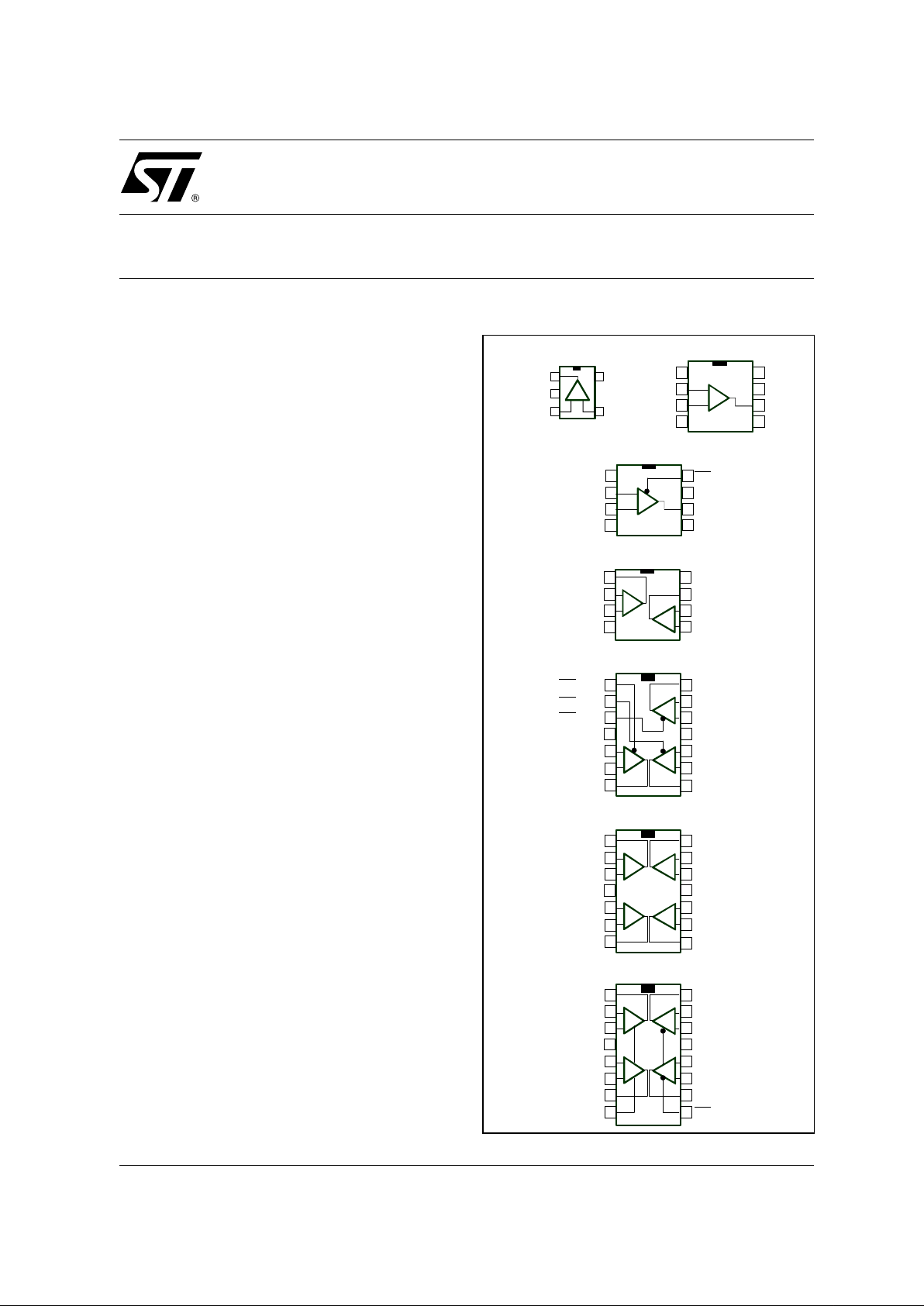
PIN CONNECTIONS (top view)
1
2
3
5
4
VCC -
VCC +
+ -
Non-Inv. In.
Inv. In.
TSH70 : SOT23-5/SO8
VCC -
VCC +
1
2
3
54
8
7
6
NC
NC
STANDBY
Non Inverting Input
Inverting Input
Output
TSH71 : SO8/TSSOP8
+
_
VCC -
VCC +
1
2
3
54
8
7
6Non Inverting Input1
Inverting Input1 Output2
+
_
Output1
Non Inverting Input2
Inverting Input2
+
_
TSH72 : SO8/TSSOP8
VCC + VCC -
1
2
3
11
4
14
13
12
Non Inverting Input1
Inverting Input1
Output3
Output1
Non Inverting Input3
Inverting Input3
5
6
7
8
10
9
+
_
+
_
+
_
Output2
Non Inverting Input2
Inverting Input2
STANDBY1
STANDBY2
STANDBY3
TSH73 : SO14/TSSOP14
VCC +
VCC -
1
2
3
114
14
13
12
Non Inverting Input2
Inverting Input2
Output4
Output2
Non Inverting Input4
Inverting Input4
5
6
7
8
10
9
+
_
+
_
+
_
Output3
Non Inverting Input3
Inverting Input3
+
_
Output1
Non Inverting Input1
Inverting Input1
TSH74 : SO14/TSSOP14
VCC +
VCC -
1
2
3
13
4
16
15
14
Non Inverting Input2
Inverting Input2
Output4
Output2
Non Inverting Input4
Inverting Input4
5
6
7
10
12
11
+
_
+
_
+
_
Output3
Non Inverting Input3
Inverting Input3
+
_
Output1
Non Inverting Input1
Inverting Input1
8
9
STANDBY
STANDBY
TSH75 : SO16/TSSOP16
Output
VCC -
VCC +
1
2
3
5
4
8
7
6
NC
NC
Output
+
_
NC
Inv. In.
Non-Inv. In.
1
2
3
5
4
VCC -
VCC +
+ -
Non-Inv. In.
Inv. In.
TSH70 : SOT23-5/SO8
VCC -
VCC +
1
2
3
54
8
7
6
NC
NC
STANDBY
Non Inverting Input
Inverting Input
Output
TSH71 : SO8/TSSOP8
+
_
VCC -
VCC +
1
2
3
54
8
7
6Non Inverting Input1
Inverting Input1 Output2
+
_
Output1
Non Inverting Input2
Inverting Input2
+
_
TSH72 : SO8/TSSOP8
VCC + VCC -
1
2
3
11
4
14
13
12
Non Inverting Input1
Inverting Input1
Output3
Output1
Non Inverting Input3
Inverting Input3
5
6
7
8
10
9
+
_
+
_
+
_
Output2
Non Inverting Input2
Inverting Input2
STANDBY1
STANDBY2
STANDBY3
TSH73 : SO14/TSSOP14
VCC +
VCC -
1
2
3
114
14
13
12
Non Inverting Input2
Inverting Input2
Output4
Output2
Non Inverting Input4
Inverting Input4
5
6
7
8
10
9
+
_
+
_
+
_
Output3
Non Inverting Input3
Inverting Input3
+
_
Output1
Non Inverting Input1
Inverting Input1
TSH74 : SO14/TSSOP14
VCC +
VCC -
1
2
3
13
4
16
15
14
Non Inverting Input2
Inverting Input2
Output4
Output2
Non Inverting Input4
Inverting Input4
5
6
7
10
12
11
+
_
+
_
+
_
Output3
Non Inverting Input3
Inverting Input3
+
_
Output1
Non Inverting Input1
Inverting Input1
8
9
STANDBY
STANDBY
TSH75 : SO16/TSSOP16
Output
VCC -
VCC +
1
2
3
5
4
8
7
6
NC
NC
Output
+
_
NC
Inv. In.
Non-Inv. In.
TSH70,71,72,73,74,75
WIDE BAND, LOW POWER OPERATIONAL AMPLIFIER
WITH STANDBY FUNCTION
August 2002

TSH70, 71, 72, 73, 74, 75
2/25
ABSOLUTE MAXIMUM RATINGS
OPERATING CONDITIONS
ORDER CODES
C = Temperature range
D = Small Outline Package (SO) - also available in Tape & Reel (DT)
P = Thin Shrink Small Outline Package (T SSOP) - only avail able in T ape
& Reel (PT)
L = Tiny Package (SOT23-5) - only available in Tape & Reel (LT)
Symbol Parameter Value Unit
V
CC
Supply Voltage
1)
14 V
V
id
Differential Input Voltage
2)
±
2V
V
i
Input Voltage
3)
±
6V
T
oper
Operating Free Air Temperature Range 0 to +70 °C
T
stg
Storage Temperature -65 to +150 °C
T
j
Maximum Junction Temperature 150 °C
R
thjc
Thermal resistance junction to case
4)
SOT23-5
SO8
SO14
SO16
TSSOPO8
TSSOP14
TSSOP16
80
28
22
35
37
32
35
°C/W
R
thja
Thermal resistance junction to ambiant area
SOT23-5
SO8
SO14
SO16
TSSOPO8
TSSOP14
TSSOP16
250
157
125
110
130
110
110
°C/W
ESD HumanBodyModel 2 kV
1. All voltages values, except differential voltage are with respect to network ground terminal
2. Differential voltages are non-inverting input terminal with respect to the inverting terminal
3. The magnitude of input and output must never exceed V
CC
+0.3V
4. Short-circuits can cause excessive heating
Symbol Parameter Value Unit
V
CC
Supply Voltage 3 to 12 V
V
IC
Common Mode Input Voltage Range
V
CC
-
to (V
CC
+
-1.1)
V
Standby
(V
CC
-
) to (V
CC
+
)
V
Type Temperature Package Marking
TSH70CLT
0°C to 70°C
SOT23-5 K301
TSH70CD SO8 70C
TSH70CDT SO8 Tape 70C
TSH71CD SO8 71C
TSH71CDT SO8 Tape 71C
TSH71CPT TSSOP8 71C
TSH72CD SO8 72C
TSH72CDT SO8 Tape 72C
TSH72CPT TSSOP8 72C
TSH73CD SO14 73C
TSH73C DT SO14 Tape 73C
TSH73CPT TSSOP14 73C
TSH74CD SO14 74C
TSH74C DT SO14 Tape 74C
TSH74CPT TSSOP14 74C
TSH75CD SO16 75C
TSH75C DT SO16 Tape 75C
TSH75CPT TSSOP16 75C

TSH70, 71, 72, 73, 74, 75
3/25
ELECTRICAL CHARACTERISTICS
V
CC
+
= 3V, V
CC
-
= GND, Vic = 1.5V, T
amb
= 25°C (unless otherwise specified)
Symbol Parameter TestCondition Min. Typ. Max. Unit
|V
io
|
Input Offset Voltage
T
amb
= 25°C
T
min.
< T
amb
< T
max.
1.2 10
12
mV
∆
V
io
Input Offset Voltage Drift vs. Temperature
T
min.
< T
amb
< T
max.
4
µ
V/°C
I
io
Input Offset Current
T
amb
= 25°C
T
min.
< T
amb
< T
max.
0.1 3.5
5
µ
A
I
ib
Input Bias Current
T
amb
= 25°C
T
min.
< T
amb
< T
max.
615
20
µ
A
C
in
Input Capacitance 0.2 pF
I
CC
Supply Current per Operator
T
amb
= 25°C
T
min.
< T
amb
< T
max.
7.2 9.8
11
mA
CMR
Common Mode Rejection Ratio
(δVic/δVio)
+0.1<Vic<+1.9V & Vout=1.5V
T
amb
= 25°C
T
min.
< T
amb
< T
max.
65
64
90 dB
SVR
Supply Voltage Rejection Ratio
(δVCC/δVio)
T
amb
= 25°C
T
min.
< T
amb
< T
max.
66
65
74
dB
PSR
Power Supply Rejection Ratio
(δVCC/δVout)
Positive & Negative Rail 75 dB
A
vd
Large Signal Voltage Gain
R
L
=150Ω to 1.5V
V
out
=1V to 2V
T
amb
= 25°C
T
min.
< T
amb
< T
max.
70
65
81
dB
I
o
Output Short Circuit Current Source
T
amb
=25°C
V
id
=+1, V
out
to 1.5V
V
id
=-1, V
out
to 1.5V
|Source|
Sink
T
min.
< T
amb
< T
max.
Vid=+1, V
out
to 1.5V
V
id
=-1, V
out
to 1.5V
|Source|
Sink
30
24
22
23
43
33
mA
V
oh
High Level Output Voltage
T
amb
=25°C
R
L
= 150Ω to GND
R
L
= 600Ω to GND
R
L
= 2kΩ to GND
R
L
= 10kΩ to GND
R
L
= 150Ω to 1.5V
R
L
= 600Ω to 1.5V
R
L
= 2kΩ to 1.5V
R
L
= 10kΩ to 1.5V
T
min.
< T
amb
< T
max.
RL = 150Ω to GND
R
L
= 150Ω to 1.5V
2.45
2.65
2.4
2.6
2.60
2.87
2.91
2.93
2.77
2.90
2.92
2.93
V

TSH70, 71, 72, 73, 74, 75
4/25
V
ol
Low Level Output Voltage
T
amb
=25°C
R
L
= 150Ω to GND
R
L
= 600Ω to GND
R
L
= 2kΩ to GND
R
L
= 10kΩ to GND
R
L
= 150Ω to 1.5V
R
L
= 600Ω to 1.5V
R
L
= 2kΩ to 1.5V
R
L
= 10kΩ to 1.5V
T
min.
< T
amb
< T
max.
RL = 150Ω to GND
R
L
= 150Ω to 1.5V
46
52
53
54
140
90
68
57
150
300
200
350
mV
GBP Gain Bandwidth Product
F=10MHz
A
VCL
=+11
A
VCL
=-10
65
55
MHz
Bw Bandwidth @-3dB
A
VCL
=+1
R
L
=150Ω to 1.5V
87 MHz
SR Slew Rate
A
VCL
=+2
R
L
=150Ω // CL to 1.5V
C
L
= 5pF
C
L
= 30pF
45
80
85
V/µs
φ
m Phase Margin
R
L
=150Ω // 30pF to 1.5V
40 °
en Equivalent Input Noise Voltage F=100kHz 11 nV/√Hz
THD Total Harmonic Distortion
A
VCL
=+2, F=4MHz
R
L
=150Ω // 30pF to 1.5V
V
out
=1Vpp
V
out
=2Vpp
-61
-54
dB
IM2 Second order intermodulation product
A
VCL
=+2, V
out
=2Vpp
R
L
=150Ω to 1.5V
Fin1=180kHz, Fin2=280KHz
spurious measurement
@100kHz
-76 dBc
IM3 Third order inter modulation product
A
VCL
=+2, V
out
=2Vpp
R
L
=150Ω to 1.5V
Fin1=180kHz, Fin2=280KHz
spurious measurement
@400kHz
-68 dBc
∆
G Differential gain
A
VCL
=+2, RL=150Ω to 1.5V
F=4.5MHz, V
out
=2Vpp
0.5 %
Df Differential phase
A
VCL
=+2, RL=150Ω to 1.5V
F=4.5MHz, V
out
=2Vpp
0.5 °
Gf Gain Flatness
F=DC to 6MHz, A
VCL
=+2
0.2 dB
Vo1/Vo2 Channel Separation F=1MHz to 10MHz 65 dB
Symbol Parameter TestCondition Min. Typ. Max. Unit

TSH70, 71, 72, 73, 74, 75
5/25
ELECTRICAL CHARACTERISTICS
V
CC
+
= 5V, V
CC
-
= GND, Vic = 2.5V, T
amb
= 25°C (unless otherwise specified)
Symbol Parameter TestCondition Min. Typ. Max. Unit
|V
io
|
Input Offset Voltage
T
amb
= 25°C
T
min.
< T
amb
< T
max.
1.1 10
12
mV
∆
V
io
Input Offset Voltage Drift vs Temperature
T
min.
< T
amb
< T
max.
3
µ
V/°C
I
io
Input Offset Current
T
amb
= 25°C
T
min.
< T
amb
< T
max.
0.1 3.5
5
µ
A
I
ib
Input Bias Current
T
amb
= 25°C
T
min.
< T
amb
< T
max.
615
20
µ
A
C
in
Input Capacitance 0.3 pF
I
CC
Supply Current per Operator
T
amb
= 25°C
T
min.
< T
amb
< T
max.
8.2 10.5
11.5
mA
CMR
Common Mode Rejection Ratio
(δVic/δVio)
+0.1<Vic<3.9V & Vout=2.5V
T
amb
= 25°C
T
min.
< T
amb
< T
max.
72
71
97 dB
SVR
Supply Voltage Rejection Ratio
(δVCC/δVio)
T
amb
= 25°C
T
min.
< T
amb
< T
max.
68
67
75
dB
PSR
Power Supply Rejection Ratio
(δVCC/δVout)
Positive & Negative Rail 75 dB
A
vd
Large Signal Voltage Gain
R
L
=150Ω to 1.5V
V
out
=1V to 4V
T
amb
= 25°C
T
min.
< T
amb
< T
max.
75
70
84
dB
I
o
Output Short Circuit Current Source
T
amb
=25°C
V
id
=+1, V
out
to 1.5V
V
id
=-1, V
out
to 1.5V
|Source|
Sink
T
min.
< T
amb
< T
max.
Vid=+1, V
out
to 1.5V
V
id
=-1, V
out
to 1.5V
|Source|
Sink
35
33
34
32
55
55
mA
V
oh
High Level Output Voltage
T
amb
=25°C
R
L
= 150Ω to GND
R
L
= 600Ω to GND
R
L
= 2kΩ to GND
R
L
= 10kΩ to GND
R
L
= 150Ω to 2.5V
R
L
= 600Ω to 2.5V
R
L
= 2kΩ to 2.5V
R
L
= 10kΩ to 2.5V
T
min.
< T
amb
< T
max.
RL = 150Ω to GND
R
L
= 150Ω to 2.5V
4.2
4.5
4.1
4.4
4.36
4.85
4.90
4.93
4.66
4.90
4.92
4.93
V

TSH70, 71, 72, 73, 74, 75
6/25
V
ol
Low Level Output Voltage
T
amb
=25°C
R
L
= 150Ω to GND
R
L
= 600Ω to GND
R
L
= 2kΩ to GND
R
L
= 10kΩ to GND
R
L
= 150Ω to 2.5V
R
L
= 600Ω to 2.5V
R
L
= 2kΩ to 2.5V
R
L
= 10kΩ to 2.5V
T
min.
< T
amb
< T
max.
RL = 150Ω to GND
R
L
= 150Ω to 2.5V
48
54
55
56
220
105
76
61
150
400
200
450
mV
GBP Gain Bandwidth Product
F=10MHz
A
VCL
=+11
A
VCL
=-10
65
55
MHz
Bw Bandwidth @-3dB
A
VCL
=+1
R
L
=150Ω to 2.5V
87 MHz
SR Slew Rate
A
VCL
=+2
R
L
=150Ω // CL to 2.5V
C
L
= 5pF
C
L
= 30pF
60
104
105
V/µs
φ
m Phase Margin
R
L
=150Ω // 30pF to 2.5V
40 °
en Equivalent Input Noise Voltage F=100kHz 11 nV/√Hz
THD Total Harmonic Distortion
A
VCL
=+2, F=4MHz
R
L
=150Ω // 30pF to 2.5V
V
out
=1Vpp
V
out
=2Vpp
-61
-54
dB
IM2 Second order intermodulation product
A
VCL
=+2, V
out
=2Vpp
R
L
=150Ω to 2.5V
Fin1=180kHz, Fin2=280kHz
spurious measurement
@100kHz
-76 dBc
IM3 Third order inter modulation product
A
VCL
=+2, V
out
=2Vpp
R
L
=150Ω to 2.5V
Fin1=180kHz, Fin2=280KHz
spurious measurement
@400kHz
-68 dBc
∆
G Differential gain
A
VCL
=+2, RL=150Ω to 2.5V
F=4.5MHz, V
out
=2Vpp
0.5 %
Df Differential phase
A
VCL
=+2, RL=150Ω to 2.5V
F=4.5MHz, V
out
=2Vpp
0.5 °
Gf Gain Flatness
F=DC to 6MHz, A
VCL
=+2
0.2 dB
Vo1/Vo2 Channel Separation F=1MHz to 10MHz 65 dB
Symbol Parameter TestCondition Min. Typ. Max. Unit
TSH70, 71, 72, 73, 74, 75
7/25
ELECTRICAL CHARACTERISTICS
V
CC
+
= 5V, V
CC
-
= -5V, Vic = GND, T
amb
= 25°C (unless otherwise specified)
Symbol Parameter Test Condition Min. Typ. Max. Unit
|V
io
|
Input Offset Voltage
T
amb
= 25°C
T
min.
< T
amb
< T
max.
0.8 10
12
mV
∆
V
io
Input Offset Voltage Drift vs Temperature
T
min.
< T
amb
< T
max.
2
µ
V/°C
I
io
Input Offset Current
T
amb
= 25°C
T
min.
< T
amb
< T
max.
0.1 3.5
5
µ
A
I
ib
Input Bias Current
T
amb
= 25°C
T
min.
< T
amb
< T
max.
615
20
µ
A
C
in
Input Capacitance 0.7 pF
I
CC
Supply Current per Operator
T
amb
= 25°C
T
min.
< T
amb
< T
max.
9.8 12.3
13.4
mA
CMR
Common Mode Rejection Ratio
(δVic/δVio)
-4.9<Vic<3.9V & Vout=GND
T
amb
= 25°C
T
min.
< T
amb
< T
max.
8180106 dB
SVR
Supply Voltage Rejection Ratio
(δVCC/δVio)
T
amb
= 25°C
T
min.
< T
amb
< T
max.
71
70
77
dB
PSR
Power Supply Rejection Ratio
(δVCC/δVout)
Positive & Negative Rail 75 dB
A
vd
Large Signal Voltage Gain
R
L
=150Ω to GND
V
out
=-4 to +4
T
amb
= 25°C
T
min.
< T
amb
< T
max.
75
70
86
dB
I
o
Output Short Circuit Current Source
T
amb
=25°C
V
id
=+1, V
out
to 1.5V
V
id
=-1, V
out
to 1.5V
|Source|
Sink
T
min.
< T
amb
< T
max.
Vid=+1, V
out
to 1.5V
V
id
=-1, V
out
to 1.5V
|Source|
Sink
35
30
34
29
55
55
mA
V
oh
High Level Output Voltage
T
amb
=25°C
R
L
= 150Ω to GND
R
L
= 600Ω to GND
R
L
= 2kΩ to GND
R
L
= 10kΩ to GND
T
min.
< T
amb
< T
max.
RL = 150Ω to GND
4.2
4.1
4.36
4.85
4.9
4.93
V
V
ol
Low Level Output Voltage
T
amb
=25°C
R
L
= 150Ω to GND
R
L
= 600Ω to GND
R
L
= 2kΩ to GND
R
L
= 10kΩ to GND
T
min.
< T
amb
< T
max.
RL = 150Ω to GND
-4.63
-4.86
-4.9
-4.93
-4.4
-4.3
mV
GBP Gain Bandwidth Product
F=10MHz
A
VCL
=+11
A
VCL
=-10
65
55
MHz
Bw Bandwidth @-3dB
A
VCL
=+1
R
L
=150Ω // 30pF to GND
100 MHz

TSH70, 71, 72, 73, 74, 75
8/25
SR Slew Rate
A
VCL
=+2
R
L
=150Ω // CL to GND
C
L
= 5pF
C
L
= 30pF
68
117
118
V/µs
φ
m Phase Margin
R
L
=150Ω to gnd
40 °
en Equivalent Input Noise Voltage F=100kHz 11 nV/√Hz
THD Total Harmonic Distortion
A
VCL
=+2, F=4MHz
R
L
=150Ω // 30pF to gnd
V
out
=1Vpp
V
out
=2Vpp
-61
-54
dB
IM2 Second order intermodulation product
A
VCL
=+2, V
out
=2Vpp
R
L
=150Ω to gnd
Fin1=180kHz, Fin2=280KHz
spurious measurement
@100kHz
-76 dBc
IM3 Third order intermodulation product
A
VCL
=+2, V
out
=2Vpp
R
L
=150Ω to gnd
Fin1=180kHz, Fin2=280KHz
spurious measurement
@400kHz
-68 dBc
∆
G Differential gain
A
VCL
=+2, RL=150Ω to gnd
F=4.5MHz, V
out
=2Vpp
0.5 %
Df Differential phase
A
VCL
=+2, RL=150Ω to gnd
F=4.5MHz, V
out
=2Vpp
0.5 °
Gf Gain Flatness
F=DC to 6MHz, A
VCL
=+2
0.2 dB
Vo1/Vo2 Channel Separation F=1MHz to 10MHz 65 dB
Symbol Parameter Test Condition Min. Typ. Max. Unit

TSH70, 71, 72, 73, 74, 75
9/25
STANDBY MODE
V
CC
+
, V
CC
-
, T
amb
= 25°C (unless otherwise specified)
Symbol Parame ter Test Condition Min. Typ. Max. Unit
Vl
ow
Standby Low Level
V
CC
-
(V
CC
-
+0.8)
V
V
high
Standby High Level
(V
CC
-
+2) (V
CC
+
)
V
I
CC SBY
Current Consumption per Operator
when STANDBY is Active
pin 8 (TSH71) to V
CC
-
pin 1,2 or 3 (TSH73) to V
CC
-
pin 8 (TSH75) to V
CC
+
pin 9 (TSH75) to V
CC
-
20 55
µ
A
Z
out
Output Impedance (Rout//Cout)
R
out
C
out
10
17
M
Ω
pF
T
on
Time from Standby Mode to Active
Mode
2
µ
s
T
off
Time from Active Mode to Standby
Mode
Down to I
CC SBY
= 10µA
10
µ
s
TSH71 STANDBY CONTROL pin 8 (SBY
) OPERATOR STATUS
V
low
Standby
V
high
Active
TSH73 STANDBY CONTROL OPERATOR STATUS
pin 1
(SBY
OP1)
pin 2
(SBY OP2)
pin 3
(SBY OP3)
OP1 OP1 OP3
V
low
x x Standby x x
V
high
x x Active x x
x
V
low
x x Standby x
x
V
high
x Active x
xx
V
low
x x Standby
xx
V
high
x x Active
TSH75 STANDBY CONTROL OPERATOR STATUS
pin 8
(SBY OP2)
pin 9
(SBY
OP3)
OP1 OP2 OP3 OP4
V
high
V
low
Active Standby Standby Active
V
high
V
high
Active Standby Active Active
V
low
V
low
Active Active Standby Active
V
low
V
high
Active Active Active Active

TSH70, 71, 72, 73, 74, 75
10/25
Closed Loop Gain and Phase vs. Frequency
Gain=+2, Vcc= ±1.5V, RL=150Ω
, T
amb
= 25°C
Closed Loop Gain and Phase vs. Frequency
Gain=-10, Vcc=
±1.5V, RL=150Ω, T
amb
= 25°C
Large Signal Measurement - Positive Slew Rate
Gain=2,Vcc=±1.5V,ZL=150Ω//5.6pF,Vin=400mVpk
Overshoot function of output capacitance
Gain=+2, Vcc=
±1.5V , T
amb
= 25°C
Closed Loop Gain and Phase vs. Frequency
Gain=+11, Vcc=
±1.5V, RL=150Ω, T
amb
= 25°C
Large Signal Measurement - Negative Slew Rate
Gain=2,Vcc=±1.5V,ZL=150Ω//5.6pF,Vin=400mVpk
1E+4 1E+5 1E+6 1E+7 1E+8 1E+9
Frequency (Hz)
-20
-15
-10
-5
0
5
10
Gain (dB)
-200
-100
0
100
200
Phase (°)
Gain
Phase
1E+4 1E+5 1E+6 1E+7 1E+8 1E+9
Frequency (Hz)
-10
0
10
20
30
Gain (dB)
-100
-50
0
50
100
150
200
Gain
Phase
Phase (°)
0 102030405060
Time (ns)
-1
-0.5
0
0.5
1
Vout (V)
1E+6 1E+7
1E+8 1E+9
Frequenc y ( Hz)
-5
0
5
10
Gain (dB)
150
Ω
150Ω//10pF
150Ω//33pF
150Ω//22pF
1E+4 1E+5 1E+6 1E+7 1E+8 1E+9
Frequency (Hz)
-10
0
10
20
30
Gain (dB)
-150
-100
-50
0
Phase (°)
Gain
Phase
0102030
40
50
Time (ns)
-1
-0.5
0
0.5
1
Vout (V)

TSH70, 71, 72, 73, 74, 75
11/25
Small Signal Measurement - Rise Time
Gain=2,Vcc=±1.5V, ZL=150Ω,Vin=400mVpk
Channel separation (Xtalk) vs frequency
Measurement configuration : Xtalk=20log(V0/V1)
Equivalent Noise Voltage
Gain=100, Vcc=±1.5V, No load
Small Signal Measurement - Fall Time
Gain=2,Vcc=±1.5V, ZL=150Ω,Vin=400mVpk
Channel separation (Xtalk) vs frequency
Gain=+11, Vcc=
±1.5V, ZL=150Ω//27pF
Maximum Output Swing
Gain=11, Vcc=±5V, RL=150Ω
0102030405060
Time (ns)
-0.06
-0.04
-0.02
0
0.02
0.04
0.06
Vin, Vout (V)
Vin
Vout
100
Ω
1k
Ω
100
Ω
1k
Ω
+
-
49.9
Ω
VO
150Ω
+
-
49.9Ω
V1
150
Ω
VIN
+
-
0.1 1 10 100 1000
Frequency (kHz)
5
10
15
20
25
30
en (nV/
√
Hz)
_
+
100
10k
0 102030405060
Time (ns)
-0.06
-0.04
-0.02
0
0.02
0.04
0.06
Vin, Vout (V)
Vin
Vout
1E+4 1E+5 1E+6 1E+7
Frequency (Hz)
-110
-100
-90
-80
-70
-60
-50
-40
-30
-20
Xtalk (dB)
3/1output
4/1output
2/1output
0.0E+0 5.0E-2 1.0E-1 1.5E-1 2.0E-1
Time (ms)
-5
-4
-3
-2
-1
0
1
2
3
4
5
Vin, Vout (V)
Vout
Vin

TSH70, 71, 72, 73, 74, 75
12/25
Standb y Mod e - To n, Tof f
Vcc=
±1.5V, Open Loop
Group De l ay
Gain =2, V cc =
±1.5V, ZL=150Ω//27pF, T
amb
= 25°C
Third Order Intermod ulatio n
Gain =2, Vcc =
±1.5V, ZL=150Ω//27pF , T
amb
= 25°C
0 2E-6 4E-6 6E-6 8E-6 1E-5
Time (s)
-2
-1
0
1
2
Vin, Vout (V)
Vout
Ton
Toff
Standby
Vin
Intermodul at io n pro ducts
The IFR2026 synthesizer generates a two
tones signal (F1=180kHz, F2=280kHz); each
tone having the same amplitude level.
The HP3585 spectrum analyzer measures the
intermodulation products function of the output
voltage. The generator and the spectrum analyzer are phase locked for precision considerations.
Group
Delay
Gain
5.87ns
01234
Vout peak(V)
-100
-90
-80
-70
-60
-50
-40
-30
-20
-10
0
IM3 (dBc)
80kHz
380kHz
640kHz
740kHz

TSH70, 71, 72, 73, 74, 75
13/25
Closed Loop Gain and Phase vs. Frequency
Gain=+2, Vcc=
±2.5V, RL=150Ω, T
amb
= 25°C
Closed Loop Gain and Phase vs. Frequency
Gain=-10, Vcc=
±2.5V, RL=150Ω, T
amb
= 25°C
Large Signal Measurement - Positive Slew Rate
Gain=2,Vcc=±2.5V,ZL=150Ω//5.6pF,Vin=400mVpk
Overshoot function of output capacitance
Gain=+2, Vcc=
±2.5V , T
amb
= 25°C
Closed Loop Gain and Phase vs. Frequency
Gain=+11, Vcc=
±2.5V, RL=150Ω, T
amb
= 25°C
Large Signal Measurement - Negative Slew Rate
Gain=2,Vcc=±2.5V,ZL=150Ω//5.6pF,Vin=400mVpk
1E+4 1E+5 1E+6 1E+7 1E+8 1E+9
Frequency (Hz)
-15
-10
-5
0
5
10
Gain (dB)
-200
-100
0
100
200
Phase (°)
Gain
Phase
1E+4 1E+5 1E+6 1E+7 1E+8 1E+9
Frequency (Hz)
-10
0
10
20
30
Gain (dB)
-100
-50
0
50
100
150
200
Phase (°)
Gain
Phase
0 1020304050607080
Time (ns)
-3
-2
-1
0
1
2
3
Vout (V)
1E+6 1E+ 7 1E+8 1E+9
Frequency (Hz)
-5
0
5
10
Gain (dB)
150
Ω
150Ω//33pF
150Ω//22pF
150Ω//10pF
1E+4 1E+5 1E+6 1E+7 1E+8 1E+9
Frequency (Hz)
-10
0
10
20
30
Gain (dB)
-150
-100
-50
0
Phase (°)
Gain
Phase
0 10203040506070
Time (ns)
-3
-2
-1
0
1
2
3
Vout (V)

TSH70, 71, 72, 73, 74, 75
14/25
Small Signal Measurement - Rise Time
Gain=2,Vcc=±2.5V,Zl=150Ω,Vin=400mVpk
Channel separation (Xtalk) vs frequency
Measurement configuration : Xtalk=20log(V0/V1)
Equivalent Noise Voltage
Gain=100, Vcc=±2.5V, No load
Small Signal Measurement - Fall Time
Gain=2,Vcc=±2.5V,Zl=150Ω,Vin=400mVpk
Channel separation (Xtalk) vs frequency
Gain=+11, Vcc=
±2.5V, ZL=150Ω//27pF
Maximum Output Swing
Gain=11, Vcc=±2.5V, RL= 150Ω
0 102030405060
Time (ns)
-0.06
-0.04
-0.02
0
0.02
0.04
0.06
Vin, Vout (V)
Vin
Vout
100
Ω
1k
Ω
100
Ω
1k
Ω
+
-
49.9
Ω
VO
150Ω
+
-
49.9Ω
V1
150
Ω
VIN
+
-
0.1 1 10 100 1000
Frequency (kHz)
5
10
15
20
25
30
en (nV/
√
Hz)
_
+
100
10k
0 102030405060
Time (ns)
-0.06
-0.04
-0.02
0
0.02
0.04
0.06
Vin Vout (V)
Vin
Vout
1E+4 1E+5 1E+6 1E+7
Frequency (Hz)
-110
-100
-90
-80
-70
-60
-50
-40
-30
-20
Xtalk (dB)
3/1output
4/1output
2/1output
0.0E+0 5.0E-2 1.0E-1 1.5E-1 2.0E-1
Time (ms)
-3
-2
-1
0
1
2
3
Vin, Vout (V)
Vout
Vin

TSH70, 71, 72, 73, 74, 75
15/25
Standb y Mod e - To n, Tof f
Vcc=
±2.5V, Open Loop
Group De l ay
Gain=2, Vcc= ±2. 5V, ZL=150Ω//27pF, T
amb
= 25°C
Third Order Intermod ulatio n
Gain=2, Vcc=
±2.5V, ZL=150Ω//27pF, T
amb
= 25°C
0 2E-64E-66E-68E-61E-5
Time (s)
-3
-2
-1
0
1
2
3
Vin, Vout (V)
Vout
Ton Toff
Standby
Vin
Intermodul at io n pro ducts
The IFR2026 synthesizer generates a two
tones signal (F1=180kHz, F2=280kHz); each
tone having the same amplitude level.
The HP3585 spectrum analyzer measures the
intermodulation products function of the output
voltage. The generator and the spectrum analyzer are phase locked for precision considerations.
Group
Delay
Gain
5.32ns
01234
Vout peak(V)
-100
-90
-80
-70
-60
-50
-40
-30
-20
-10
0
IM3 (dBc)
740kHz
380kHz
640kHz
80kHz

TSH70, 71, 72, 73, 74, 75
16/25
Closed Loop Gain and Phase vs. Frequency
Gain=+2, Vcc=
±5V, RL=150Ω, T
amb
= 25°C
Closed Loop Gain and Phase vs. Frequency
Gain=-10, Vcc=
±5V, RL=150Ω, T
amb
= 25°C
Large Signal Measurement - Positive Slew Rate
Gain=2,Vcc=±5V,ZL=150Ω//5.6pF,Vin=400mVpk
Overshoot function of output capacitance
Gain=+2, Vcc=
±5V, T
amb
= 25°C
Closed Loop Gain and Phase vs. Frequency
Gain=+11, Vcc=
±5V, RL=150Ω, T
amb
= 25°C
Large Signal Measurement - Negative Slew Rate
Gain=2,Vcc=±5V,ZL=150Ω//5.6pF,Vin=400mVpk
1E+4 1E+5 1E+6 1E+7 1E+8 1E+9
Frequency (Hz)
-15
-10
-5
0
5
10
Gain (dB)
-200
-100
0
100
200
Phase (°)
Gain
Phase
1E+4 1E+5 1E+6
1E+7 1E+8
1E+9
Frequency (Hz)
-10
0
10
20
30
Gai n (dB)
-50
0
50
100
150
200
Phase (°)
Gain
Phase
0 20406080100
Time (ns)
-5
-4
-3
-2
-1
0
1
2
3
4
5
Vout (V)
1E+6 1E+7 1E+8 1E+9
Frequency (Hz)
-5
0
5
10
Gain (dB)
150
Ω
150Ω//10pF
150Ω//33pF
150Ω//22pF
1E+4 1E+5 1E+6 1E+7 1E+8 1E+9
Frequency (Hz)
-10
0
10
20
30
Gain (dB)
-150
-100
-50
0
Phase (°)
Gain
Phase
0 20406080100
Time (ns)
-5
-4
-3
-2
-1
0
1
2
3
4
5
Vout (V)

TSH70, 71, 72, 73, 74, 75
17/25
Small Signal Measurement - Rise Time
Gain=2,Vcc =±5V,ZL=150Ω, V in=400mVpk
Channel separation (Xtalk) vs frequency
Measurement configuration : Xtalk=20log(V0/V1)
Equivalent Noise Voltage
Gain=100, Vcc=±5V, No load
Small Signal Measurement - Fall Time
Gain=2,Vcc=±5V,ZL=150Ω,Vin=400mVpk
Channel separation (Xtalk) vs frequency
Gain=+11, Vcc=
±5V, ZL=150Ω//27pF
Maximum Output Swing
Gain=11, Vcc=±5V, RL=150Ω
0 102030405060
-0.06
-0.04
-0.02
0
0.02
0.04
0.06
Vin, Vout (V)
Vin
Vout
Time (ns)
100Ω
1k
Ω
100
Ω
1k
Ω
+
-
49.9
Ω
VO
150Ω
+
-
49.9Ω
V1
150
Ω
VIN
+
-
0.1 1 10 100 1000
Frequency (kHz)
5
10
15
20
25
30
en (nV/
√
Hz)
_
+
100
10k
0 102030405060
Time (ns)
-0.06
-0.04
-0.02
0
0.02
0.04
0.06
Vin, Vout (V)
Vin
Vout
1E+4 1E+5 1E+6
1E+7
Frequency (Hz)
-110
-100
-90
-80
-70
-60
-50
-40
-30
-20
Xtalk (dB)
3/1output
4/1output
2/1output
0.0E+0 5.0E-2 1.0E-1 1.5E-1 2.0E-1
Time (ms)
-5
-4
-3
-2
-1
0
1
2
3
4
5
Vin, Vout (V)
Vout
Vin

TSH70, 71, 72, 73, 74, 75
18/25
Standb y Mod e - To n, Tof f
Vcc=
±5V, Open Loop
Group De l ay
Gain=2, Vcc=±5V, ZL=150Ω//27pF, T
amb
= 25°C
Third Order Intermod ulatio n
Gain=2, Vcc=
±5V, ZL=150Ω//27pF, T
amb
= 25°C
0 2E-6 4E-6 6E-6 8E-6
Time (s)
-5
0
5
Vin, Vout (V)
Vout
Standby
Ton Toff
Vin
Intermodul at io n pro ducts
The IFR2026 synthesizer generates a two
tones signal (F1=180kHz, F2=280kHz); each
tone having the same amplitude level.
The HP3585 spectrum analyzer measures the
intermodulation products function of the output
voltage. The generator and the spectrum analyzer are phase locked for precision considerations.
Group
Delay
Gain
5.1ns
01234
Vout peak( V)
-100
-90
-80
-70
-60
-50
-40
-30
-20
-10
0
IM3 (dBc)
80kHz
380kHz
640kHz
740kHz

TSH70, 71, 72, 73, 74, 75
19/25
TESTING CONDITIONS:
Layout precautions:
To use the TSH7X circuits in the best manner at
high frequencies, some precautions have to be
taken for power supplies:
- First of all, the implementation of a proper ground
plane in both sides of the PCB is mandatory for
high speed circuit applications to provide low inductance and low resistance common return.
- Power supply bypas s capacitors (4.7uF and c eramic 100pF) should be placed as close as poss ible to the IC pins in order to improve high frequency bypassing and reduce harmonic distortion. The
power supply capa citors must be incorporated for
both the negative and the positive pins.
- Proper termination of all inputs and outputs must
be in accordance with output termination resistors;
then the amplifier load wi ll be only resistive and
the stab ilit y of the a m p li fier will be impro v ed.
All leads must be wide and as s hort as possible
especially for op amp inputs and outputs in order
to decrease parasitic capacitance and inductance.
- For lower gain application, a ttention should be
paid not to use large feedback resist ance (>1kΩ)
to reduce time constant with parasitic capacitances.
- Choose component sizes as small as possible
(SMD).
- Finally, on output, the load capacitance must be
negligible to maintain good stability. You can put a
serial resistance the closest to the output pin to
minimize its influence.
CCIR330 video line
Maximum input level:
The input level m us t not exce ed the f oll owing values:
❑ negative peak: must be greater than
-Vcc+400mV.
❑ positive peak value: must be lower than
+Vcc-400mV.
The electrical characteristics show the influence of
the load on this parameter.
Video capabilities:
To characterize the differential phase and differential gain a CCIR330 video line is used.
The video line contains 5 (flat) levels of luma on
which is superimposed chroma signal. (the first
level contains no luma). T he luma gives va rious
amplitudes which def ine the sat uration of the signal. The chrominance gives various phases which
define the colour of the signal.
Differential phase (respectively differential gain)
distortion is present if a signal chrominance phase
(gain) is affected by luminance level. They represent the ability to uniformly process the high frequency information at all luminance levels.
When differential gain is present, colour saturation
is not correctly reproduced.
The input generator is the Rohde & Schwarz
CCVS. The output measurement is done by the
Rohde and Schwarz VSA.
Measurement on Rohde and Schwarz VSA.

TSH70, 71, 72, 73, 74, 75
20/25
Video Results:
Precautions on asymme trical suppl y
operation:
The TSH7X can be used either with a dual or a
single supply. If a single supply is used, the inputs
are biased to the mid-supply voltage (+Vcc/2).
This bias network must be carefully des igned, in
order to reject any noise present on the supply rail.
As the bias current is 15uA, you must carefully
choose the resistance R1 not to introduce an offset mismatch at the amplifier inputs.
R1=10KΩ will be conv enient. C1, C2, C3 are bypass capacitors from perturbation on Vcc as well
as for the input and output signals. We choose
C1=100nF and C2=C3=100uF .
R2, R3 are such that the current through them
must be superior to 100 times the bias current. So,
we take R2=R3=4.7KΩ.
Cin, as Cout are chosen to filter the DC s ignal by
the lowpass filters (R1,Cin) and (Rout, Cout). By
taking R1=10KΩ, RL=150Ω, and Cin=2uF,
Cout=220uF we provide a c utoff frequency bel ow
10Hz.
Use of the TSH7X in gain=-1 configuration:
Some precautions hav e to be added, specially for
low power supply application.
A feedback capac itance Cf sho uld be added for
better stability. The table summ arizes the impact
of the capacitance Cf on the phase margin of the
circuit.
Parameter
Value
Vcc=+-2.5V
Value
Vcc=+-5V
Unit
Lum NL 0.1 0.3 %
Lum NL Step 1 100 100 %
Lum NL Step 2 100 99.9 %
Lum NL Step 3 99.9 99.8 %
Lum NL Step 4 99.9 99.9 %
Lum NL Step 5 99.9 99.7 %
Diff Gain pos 0 0 %
Diff Gain neg -0.7 -0.6 %
Diff Gain pp 0.7 0.6 %
Diff Gain Step1 -0.5 -0.3 %
Diff Gain Step2 -0.7 -0.6 %
Diff Gain Step3 -0.3 -0.5 %
Diff Gain Step4 -0.1 -0.3 %
Diff Gain Step5 -0.4 -0.5 %
Diff Phase pos 0 0.1 deg
Diff Phase neg -0.2 -0.4 deg
Diff Phase pp 0.2 0.5 deg
Diff Phase Step1 -0.2 -0.4 deg
Diff Phase Step2 -0.1 -0.4 deg
Diff Phase Step3 -0.1 -0.3 deg
Diff Phase Step4 0 0.1 deg
Diff Phase Step5 -0.2 -0.1 deg
IN
R1
Vcc+
OUT
R2
R3
C1
C3
C2
Cin
Cout
+
-
Cf
R5
R4
RL
IN
R1
Vcc+
OUT
R2
R3 C1C3C2
Cin
Cout
+
-
1k
Cf
1k
RL

TSH70, 71, 72, 73, 74, 75
21/25
Example of a video application :
This example shows a possible application of the TSH7X circuit. Here, you can multiplex the channels for
the different standard PAL, NTSC as you filter for the different bands; the video signal can be filtered with
two different cutoff frequencies, corresponding to a PAL encoded signal (LPF1) or a NTSC signal (LPF2).
You can multiplex input signals, as the outputs are in high impedance state in standby mode.This enables
you, to use a PAL filter as the Standby mode is active and to use the NTSC filter otherwise.
The video application requires 1Vpeak at input and output.
Calculation of components:
A decoupling capacitor is provided to cutoff the frequencies below 10Hz according I bias.Hence Ce=10uF,
with Rb1=10KΩ. At the output, Cout=220uF.
The AOP1 is in 6dB configuration for the adaptation bridge. R1=R2=1KΩ.V1=2Vpk. V2=1Vpk
For the PAL communication, we need a lowpass filtering. The load resistance R4 is function of the output
resistance of the filter.V3=V2/A1 where A1 is the attenuation factor of the filter LPF1.
To compensate the filter insertion loss, we add an additional factor to the gain of the 2nd amplifier AOP2.
For example, f or an attenuation of 3dB, w e choose R5=300Ω and R6=1KΩ. We have V4=2Vpk and
Vout=1Vpk.
The calculation of the parameters R7, C7, R8, C8, R9, R10 will be exactly the same .
Parameter Cf (pF) Vcc=!1.5V Vcc=!2.5V Vcc=!5V Unit
Phase Margin
0
28 43 56 deg
f-3dB 40 39.3 38.3 MHz
Phase Margin
5.6
30 43 56 deg
f-3dB 40 39.3 38.3 MHz
Phase Margin
22
37 52 67 deg
f-3dB 37 34 32 MHz
Phase Margin
33
48 65 78 deg
f-3dB 33.7 30.7 27.6 MHz
IN
Ce
Re
Rb1
Vcc/2
+
-
Vcc/2
+
-
+
-
Standby
Standby
R1
R2
R3 C3
R4
C4
Rb1
R5
R6
R9
R10
Rout
OUT
AOP1
AOP2
AOP3
V1
V2 V3
V4
A1
Vcc/2
Vcc/2
Cf
Cf
Cf
Cout
Vcc/2
RL
R7 C7
R8
C8
LPF2
A2
PAL
NTSC
LPF1
Rb1
Vcc/2

TSH70, 71, 72, 73, 74, 75
22/25
PACKAGE MECHANICAL DATA
8 PINS - PLASTIC MICROPACKAGE (SO)
PACKAGE MECHANICAL DATA
8 PINS - THIN SHRINK SMALL OUTLIN E
PACKAGE (TSSOP)
Dim.
Millimeters Inches
Min. Typ. Max. Min. Typ. Max.
A 1.75 0.069
a1 0.1 0.25 0.004 0.010
a2 1.65 0.065
a3 0.65 0.85 0.026 0.033
b 0.35 0.48 0.014 0.019
b1 0.19 0.25 0.007 0.010
C 0.25 0.5 0.010 0.020
c1 45° (typ.)
D 4.8 5.0 0.189 0.197
E 5.8 6.2 0.228 0.244
e 1.27 0.050
e3 3.81 0.150
F 3.8 4.0 0.150 0.157
L 0.4 1.27 0.016 0.050
M 0.6 0.024
S 8° (max.)
Dim.
Millimeters Inches
Min. Typ. Max. Min. Typ. Max.
A 1.20 0.05
A1 0.05 0.15 0. 01 0.006
A2 0.80 1.00 1.05 0.031 0.039 0.041
b 0.19 0.30 0.0 07 0.15
c 0.09 0.20 0.003 0.0 12
D 2.90 3.00 3.10 0.114 0.118 0.122
E 6.40 0.252
E1 4.30 4.40 4.50 0.169 0.173 0.177
e 0.65 0.025
k0° 8°0° 8°
l 0.50 0.60 0.75 0. 09 0.0236 0.030
C
L
14
8
5
L1
c
0.25mm
.010 inch
GAGE PLANE
E1
k
L
L1
E
SEATING
PLANE
A
A2
D
A1
b
5
8
4
1
PIN 1 IDENTIFICATION
e

TSH70, 71, 72, 73, 74, 75
23/25
PACKAGE MECHANICAL DATA
14 PINS - PLASTIC MICROPACKAGE (SO)
PACKAGE MECHANICAL DATA
14 PINS - THIN SHRINK SMALL OUTLINE
PACKAGE (TSSOP)
Dim.
Millimeters Inches
Min. Typ. Max. Min. Typ. Max.
A 1.75 0.069
a1 0.1 0.2 0.004 0.008
a2 1.6 0.063
b 0.35 0.46 0.014 0.018
b1 0.19 0.25 0.007 0.010
C 0.5 0.020
c1 45° (typ.)
D (1) 8.55 8.75 0.336 0.344
E 5.8 6.2 0.228 0.244
e 1.27 0.050
e3 7.62 0.300
F (1) 3.8 4.0 0.150 0.157
G 4.6 5.3 0.181 0.208
L 0.5 1.27 0.020 0.050
M 0.68 0.027
S 8° (max.)
Note : (1) D and F do not include mold flash or protr usions - Mold f lash
or protrusions shall not exceed 0.15mm (.066 inc) ONLY FOR DATA
BOOK.
D
M
F
14
1
7
8
b
e3
e
E
LG
C
c1
A
a2
a1
b1
s
Dim.
Millimeters Inches
Min. Typ. Max. Min. Typ. Max.
A 1.20 0.05
A1 0.05 0.15 0.01 0.006
A2 0.80 1.00 1.05 0.031 0.039 0.041
b 0.19 0.30 0.007 0.15
c 0.09 0.20 0.003 0.012
D 4.90 5.00 5.10 0.192 0.196 0.20
E 6.40 0.252
E1 4.30 4.40 4.50 0.169 0.173 0.177
e 0.65 0.025
k0° 8°0° 8°
l 0.50 0.60 0.75 0.09 0.0236 0.030
c
E1
k
L
E
e
b
D
PIN 1IDENTIFICATION
1
78
14
SEATING
PLANE
C
aaa
C
0,25 mm
.010 inch
GAGE PLANE
L1
A
A2
A1

TSH70, 71, 72, 73, 74, 75
24/25
PACKAGE MECHANICAL DATA
16 PINS - PLASTIC MICROPACKAGE (SO)
PACKAGE MECHANICAL DATA
16 PINS - THIN SHRINK SMALL OUTLINE
PACKAGE (TSSOP)
Dim.
Millimeters Inches
Min. Typ. Max. Min. Typ. Max.
A 1.75 0.069
a1 0.1 0.2 0.004 0.008
a2 1.6 0.063
b 0.35 0.46 0.014 0.018
b1 0.19 0.25 0.007 0.010
C 0.5 0.020
c1 45° (typ.)
D 9.8 10 0.386 0.394
E 5.8 6.2 0.228 0.244
e 1.27 0.050
e3 8.89 0.350
F 3.8 4.0 0.150 0.157
G 4.6 5.3 0.181 0.209
L 0.5 1.27 0.020 0.050
M 0.62 0.024
S 8° (max.)
Dim.
Millimeters Inches
Min. Typ. Max. Min. Typ. Max.
A 0 .90 1.20 1.45 0.035 0.047 0.057
A1 0 0.1 5 0.0 06
A2 0.90 1.05 1.30 0.035 0.041 0.051
B 0 .35 0.40 0.50 0.014 0.016 0.020
C 0.09 0.15 0.20 0.004 0.006 0.008
D 2.80 2.90 3.00 0.110 0.114 0.118
D1 1.90 0. 075
e 0.95 0.037
E 2 .60 2.80 3.00 0.102 0.110 0 .0118
F 1.50 1.60 1.75 0.059 0.063 0.069
L 0.10 0.5 0.60 0.004 0. 014 0.024
c
E1
k
L
E
e
b
D
PIN 1 IDENTIFICATION
1
89
16
SEATING
PLANE
C
aaa
C
0,25 mm
.010 inch
GAGE PLANE
L1
A
A2
A1

TSH70, 71, 72, 73, 74, 75
25/25
Information furnished is beli eved to be accurate and reliable. However, STMicroe lectronics assumes no responsibility for the
consequences of use of such information nor for any infringement of patents or other rights of third parties which may result from
its use. No licens e is granted by implication or otherwise unde r any patent or pate nt rights of STMicroelectronics. Specifications
mentioned in this publication ar e subject to change without notice. This publication supersedes and replaces all information
previously supplied. S TMicroelectronics products are not authorized for use as critica l components in life suppo rt devices or
systems without express written approval of STMicroelectronics.
© The ST logo is a registered trademark of STMicroelectronics
© 2002 STM i cr o electro n ics - Printed in Italy - All Rights Res er ved
STMicr oelectronics GROUP OF COMP ANIES
Australi a - Brazil - Canada - Chin a - F i nl and - Franc e - Germany - Hong Kong - Ind i a - Is rael - Ital y - Japan - Malay sia
Malta - Mor occo - Singapore - Spain - Sweden - Swi tzerland - United Kingdom - United States
© http://www.st.com
PACKAGE MECHANICAL DATA
5 PINS - TINY PACKAGE (SOT23)
Dim.
Millimeters Inches
Min. Typ. Max. Min. Typ. Max.
A 0.90 1.20 1.45 0.035 0.047 0.057
A1 0 0.15 0.006
A2 0.90 1.05 1.30 0.035 0.041 0.051
B 0.35 0.40 0.50 0.014 0.016 0.020
C 0.09 0.15 0.20 0.004 0.006 0.008
D 2.80 2.90 3.00 0.110 0.114 0.118
D1 1.90 0.075
e 0.95 0.037
E 2.60 2.80 3.00 0.102 0.110 0.0118
F 1.50 1.60 1.75 0.059 0.063 0.069
L 0.10 0.5 0.60 0.004 0.014 0.024
K 0d 10d 0d 10d
L
C
F
A2
A
A1
B
E
D D1
E
 Loading...