

SGS Thomson Microelectronics TSH691ID Datasheet
LOW COST 40MHz - 1GHz AMPLIFIER
.
28dB GAIN @3V @ 450MHz
.
+13.5dBmOUTPUTPOWER(P1dB)
.
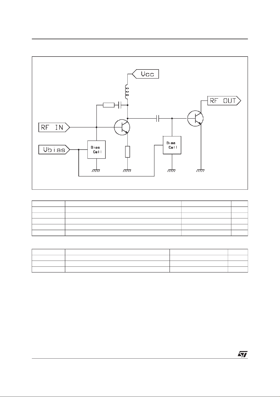
BIASPIN FOR OUTPUTPOWER& AMPLIFIER DISABLE
.
50Ω INPUT/OUTPUTMATCHING
DESCRIPTION
TSH691 is a low cost RF amplifier consisted of 2
stages,designedin advancedbipolarprocess, featuring high performances.Anexternal bias current
adjust allowsto tunethe outputpower and also to
settheamplifierinpower-downmode.TheTSH691
is intended to RF consumer equipments in ISM
band (remote controls, ASK transmitters) where
cost issensitive
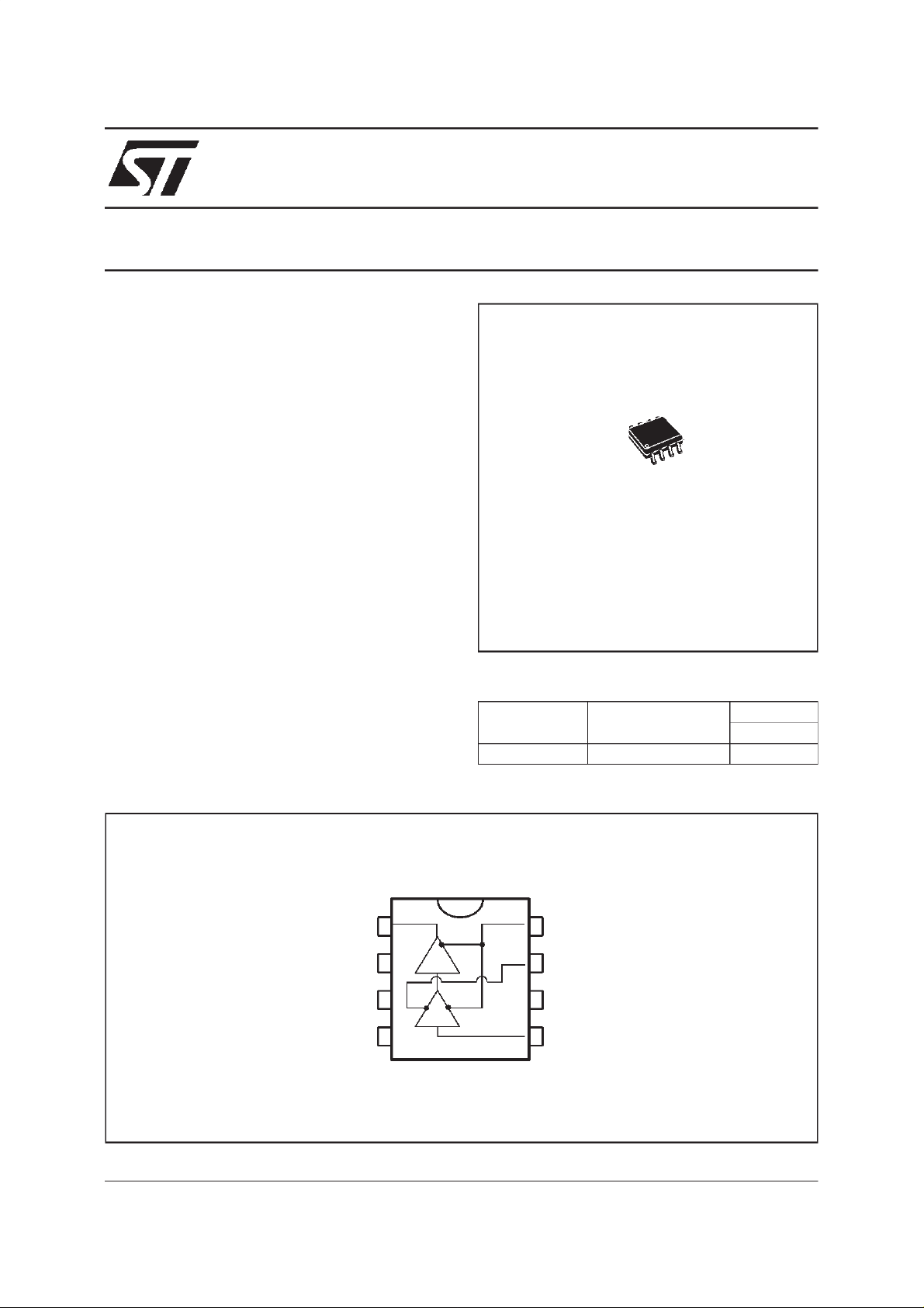
D
SO8
(Plastic Micropackage)
ORDER CODES
Part Number Temperature Range
o
TSH691ID -35, +85
C •
TSH691
Package
D
PIN CONNECTIONS (top view)
RF out
June 1998
GND
GND
GND
1
2
3
4
8
7
6
5
Vbias
V
CC
GND
RF in
1/10
TSH691
SCHEMATIC DIAGRAM
ABSOLUTE MAXIMUMRATINGS
Symbol Parameter Value Unit
V
CC1,VCC2,Vbias
RF in RF Input Power +10 dBm
RF out RF Output Power +21 dBm
T
oper
T
stg
Supply Voltages & Bias Voltage 5.5 V
Operating Free Air Temperature Range -35 to +85
Storage Temperature Range -65 to +150
OPERATINGCONDITIONS
Symbol Parameter Value Unit
V
CC1,VCC2,Vbias
V
bias
RF
sr
Supply Voltages 1.5 to 5 V
Bias Voltage 0to 6 V
RF Signal Range 40 to 1000 MHz
ESD SENSITIVEDEVICE
Handling Precautions Required
o
C
o
C
2/10

ELECTRICAL CHARACTERISTICS
=25oC, VCC&V
T
amb
=+2.7V,ZL=50Ω
bias
TSH691
Parameter
SupplyCurrent 46 mA
S21 (V
S21 (Vin= -20dBm, f = 900MHz) 17 dB
Output Power 1dB Compression (f = 450MHz) 12 dBm
3rd Order Intercept Point (f = 430MHz) 22 dBm
S12 (Reverse Isolation @ f = 400MHz) -46 dB
S11 (Input Return Loss @ f =450MHz) -15 dB
S11 (Input Return Loss @ f =900MHz) -10 dB
Noise Figure @ f = 450MHz 4.5 dB
Noise Figure @ f = 900MHz 5.4 dB
R
All parameters with min. ormax. figures are 100% tested.
= -20dBm, f = 450MHz) 20 23 30 dB
in
Junction Ambient Thermal Resistance For SO8 Package 140 180
th(j-a)
Min. Typ. Max.
TSH691
o
SO8 PACKAGE THERMAL RESISTIVITY
Tamb (°C)
150
135
120
105
90
75
60
45
30
DEVICE
OVERSTRESSED
RIGHT BEHAVIOUR
Rthmin
Rthmax
Unit
C/W
123456
DEFINITION
R
th(j-a)
(oC) Maximum Die JuntionTemperature
T
j
T
amb
P
(W) Maximum DissipatedPower
d
JunctionAmbientThermalResistance
o
(~ 150
C)
(oC) Ambient Temperature
(P
= 0.75 VCC• ICC)
d
Vcc (V)
REMARKS
The right behaviour is obtained when the following equation is fulfilled.
T
j-Tamb=Pd•Rth(j-a)
3/10
 Loading...