

TSH512
TSH512
HiFi stereo/mono infrared transmitter
HiFi stereo/mono infrared transmitter
Stereo sub-carrier gen er ator
Stereo sub-carrier gen er ator
■ Supply voltage: 2.3V to 5.5V
■ Carriers frequency range: 0.4 to 11 MHz
■ High versatility: I/O pins for each section
■ Two FM transmitters for stereo
■ Sinusoidal carriers for high spectral purity
■ Micro or line level preamplifiers with ALC
■ VOX function to save on battery power
■ Transmitter 2 Standby for mono operation
DESCRIPTION
The TSH512 is a 0.4 to 11 MHz dual FM transmitter. Access pins to each section give a high versatility and allow several applica tions: stereo headphone, multimedia headset, audio sub-carrier
generator.
The TSH512 integrates in one chip:
Low-noise audio preamplifiers with ALC (Automatic Level Control), frequency modulated oscillators,
and linear output buffers to drive external tr ansistors. The sinusoidal carriers facilitates the filtering
and allows high performance audio transmission.
The VOX (Voice Op erated Transmit) circui try disables the output buffer when there is no audio t o
save battery power.
For MONO applications, the STAND-BY pin enables one transmitter only, reducing the supply
current.
The TSH512 forms a chipse t with the dua l receiver TSH511.
APPLICATIONS
■ Infrared HiFi stereo transmitter
■ Infrared Headsets
■ Stereo sub-carrier for video transmitters
■ Voice operated wireless webcams
■ FM IF transmit systems
ORDER CODE
Part Number
TSH512CF -40°C to
TSH512CFT -40°C to
Temperature
Range
+85°C
+85°C
Package Conditionning Marking
TQFP44 Tray TSH512C
TQFP44 Tape & reel TSH512C
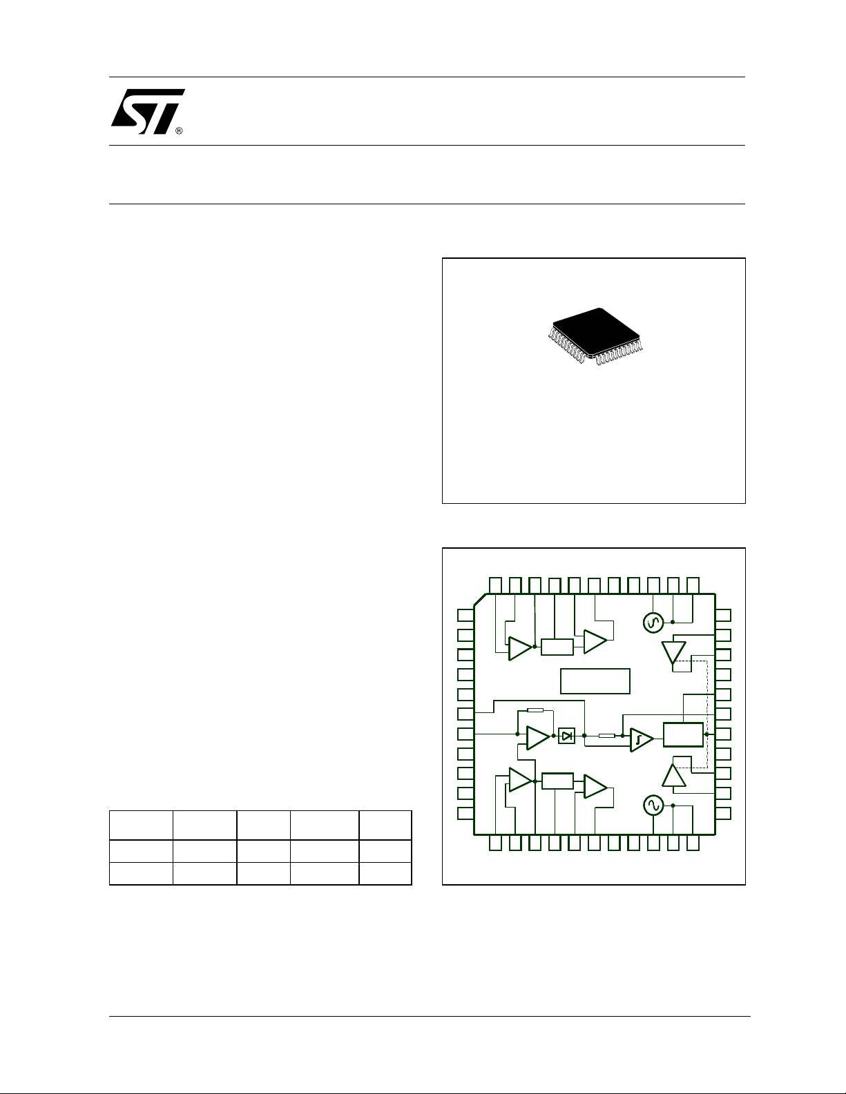
PACKAGE
F
TQFP44
10 x 10 mm
PIN CONNECTION (top view)
40
40
39
41424344
39
41424344
1
1
2
2
3
3
4
4
5
5
6
6
7
7
8
8
9
9
10
10
11
11
+
+-+
-
-
ALC
ALC
LNA
LNA
+
+-+
-
-
LNA
LNA
+
+-+
ALC
ALC
-
-
12 13 14 15 16 17 18 19 20 21 22
12 13 14 15 16 17 18 19 20 21 22
PEA
PEA
+
+-+
-
-
TX2
TX2
TSH512
TSH512
VOX
VOX
TX1
TX1
+
+-+
-
-
PEA
PEA
3738
3738
VCO
VCO
VCO
VCO
36
36
Output
Output
buffer
buffer
Output
Output
buffer
buffer
3435
3435
Monostable
Monostable
33
33
32
32
31
31
30
30
29
29
28
28
27
27
26
26
25
25
24
24
23
23
December 2002
1/19
TSH512
ABSOLUTE MAXIMUM RATINGS
Symbol Parameter Value Unit
Vcc
Supply voltage
Toper Operating free air temperature range -40 to +85 °C
Tstg Storage temperature -65 to +150 °C
Tj Maximum junction temperature 150 °C
Rthjc Thermal resistance juncti on to case 14 °C/W
Latch-up
Class
2)
ESD sensitive device: handling precautions required
ESD
except pin
20 & 36
1. All voltage s values, ex cept differential volt age, are wi th respect to network grou nd terminal
2. Corporate ST Microelectr oni cs proced ure number 0018695
3. ElectroS tatic Disch arge pulse (E SD pulse) sim ul ating a human body discharge of 10 0 pF through 1.5k
4. Discharge to Ground of a device that has been previously charged.
5. ElectroS tatic Disch arge pulse (E SD pulse) approximati ng a pulse of a ma chine or mec hanical equi pment.
HBM: Human Body Model
CDM: Charged Device Model
MM: Machine Model
OPERATING CONDITIONS
Symbol Parameter Value Unit
Vcc Supply voltage 2.3 to 5.5 V
f
audio
f
carrier
Audio frequency range 20 to 20,000 Hz
Carrier frequency range 0.4 to 11 MHz
1)
7V
A
3)
4)
5)
2
1
0.2
Ω
kV
BLOC DIAGRAM
VCO-OUT2
VCO-OUT2
VCO-A2
VCO-A2
VCO-A2
Monostable
Monostable
Monostable
VCO-A1
VCO-A1
VCO-A1
VCO-OUT2
VCO-B2
VCO-B2
VCO-B2
3435
3435
3435
GND
GND
GND
33
33
33
32
32
32
BUF-IN2
BUF-IN2
BUF-IN2
BUF-OUT2
BUF-OUT2
BUF-OUT2
31
31
31
GND
GND
GND
30
30
30
VOX-TIMER
VOX-TIMER
VOX-TIMER
29
29
29
28
28
28
VOX-INTN
VOX-INTN
VOX-INTN
27
27
27
VOX-MUTE
VOX-MUTE
VOX-MUTE
VCC
VCC
VCC
26
26
26
BUF-OUT1
BUF-OUT1
BUF-OUT1
25
25
25
24
24
24
BUF-IN1
BUF-IN1
BUF-IN1
GND
GND
GND
23
23
23
VCO-B1
VCO-B1
VCO-B1
VCO-OUT1
VCO-OUT1
VCO-OUT1
DEC2
DEC2
DEC2
MIC-BIAS2
MIC-BIAS2
MIC-BIAS2
GND
GND
GND
VCC
VCC
VCC
SBY
SBY
SBY
VOX-INTS
VOX-INTS
VOX-INTS
VOX-SENS
VOX-SENS
VOX-SENS
VCC
VCC
VCC
GND
GND
GND
MIC-BIAS1
MIC-BIAS1
MIC-BIAS1
DEC1
DEC1
DEC1
VCO-BIAS2
VCO-BIAS2
PEA-INN2
PEA-INN2
PEA-INN2
PEA-INN1
PEA-INN1
PEA-INN1
-
-
-
+
+
+-+
-
-
-
PEA-OUT2
PEA-OUT2
PEA-OUT2
PEA
PEA
PEA
+
+
+-+
VOX
VOX
VOX
PEA
PEA
PEA
PEA-OUT1
PEA-OUT1
PEA-OUT1
Bias
Bias
BiasBias
TX2
TX2
TX2
TX1
TX1
TX1
Bias
Bias
BiasBias
VCO-BIAS2
VCO-BIAS1
VCO-BIAS1
VCO-BIAS1
3738394041
3738394041
3738394041
VCC
VCC
VCC
VCO
VCO
VCO
VCO
VCO
VCO
VCC
VCC
VCC
36
36
36
Output
Output
Output
buffer
buffer
buffer
Output
Output
Output
buffer
buffer
buffer
ALC-INT2
ALC-INT2
ALC-INT2
LNA-OUT2
LNA-OUT2
LNA-OUT2
LNA-INP2
LNA-INN2
LNA-INP2
LNA-INN2
LNA-INP2
LNA-INN2
424344
424344
424344
1
1
1
2
2
2
3
3
3
4
4
4
5
5
5
6
6
6
7
7
7
8
8
8
9
9
9
10
10
10
11
11
11
+
+
+-+
-
-
-
ALC
ALC
ALC
LNA
LNA
LNA
Bias
Bias
BiasBias
Bias
Bias
BiasBias
LNA
LNA
LNA
+
+
+-+
-
-
-
12
12
12
13 14 15 16 17 18 19 20 21 22
13 14 15 16 17 18 19 20 21 22
13 14 15 16 17 18 19 20 21 22
LNA-INP1
LNA-INP1
LNA-INP1
LNA-INN1
LNA-INN1
LNA-INN1
+
+
+-+
-
-
-
LNA-OUT1
LNA-OUT1
LNA-OUT1
TSH512
TSH512
TSH512
ALC
ALC
ALC
ALC-I NT1
ALC-I NT1
ALC-I NT1
2/19
PIN DESCRIPTION
TSH512
Pin Pin name related to
1 DEC2 TX2 - Decoupling capacitor for internal voltage reference
2 MIC-BIAS2 TX2 O Microphone bias
3 GND - - GROUND
4 VCC - - SUPPLY VOLTAGE
5 SBY TX1 & TX2 I Standby Control (INPUT pin)
6 VOX-INTS TX1 & TX2 - Time constant terminal for Audio Signal integrator in VOX
7 VOX-SENS TX1 & TX2 - Gain adjustment for VOX input sensitivity
8 VCC - - SUPPLY VOLTAGE
9 GND - - GROUND
10 MIC-BIAS1 TX1 O Microphone bias
11 DEC1 TX1 - Decoupling capacitor for internal voltage reference
12 LNA-INP1 TX1 I LNA positive input
13 LNA-INN1 TX1 I LNA negative input
14 LNA-OUT1 TX1 O LNA output
15 ALC-INT1 TX1 - Time constant terminal for integrator in ALC
16 PEA-INN1 TX1 I Pre-Emphasis Amplifier negative input
17 PEA-OUT1 TX1 O Pre-Emphasis Amplifier output
18 VCO-BIAS1 TX1 O Bias for external VCO components
19 VCC - - Supply Voltage
20 VCO-A1 TX1 - Oscillator component connection
21 VCO-B1 TX1 - Oscillator component connection
22 VCO-OUT1 TX1 O VCO output
23 GND - - Ground
24 BUF-IN1 TX1 I Input to the output buffer
25 BUF-OUT1 TX1 O Output of the output buffer
26 VCC - - Supply Voltage
27 VOX-MUTE TX1 & TX2 O Mute control (Output pin) in VOX
28 VOX-INTN TX1 & TX2 - Time constant terminal for Noise integrator in VOX
29 VOX-TIMER TX1 & TX2 - Rise time for timer in VOX
30 GND - - Ground
31 BUF-OUT2 TX2 O Output of the output buffer
32 BUF-IN2 TX2 I Input to the output buffer
33 GND - - Ground
34 VCO-OUT2 TX2 O VCO output
35 VCO-B2 TX2 - Oscillator component connection
36 VCO-A2 TX2 - Oscillator component connection
37 VCC - - Supply Voltage
38 VCO-BIAS2 TX2 O Bias for external VCO components
39 PEA-OUT2 TX2 O Pre-Emphasis Amplifier output
40 PEA-INN2 TX2 I Pre-Emphasis Amplifier negative input
41 ALC-INT2 TX2 - Time constant terminal for internal peak detector in ALC
42 LNA-OUT2 TX2 O LNA output
43 LNA-INN2 TX2 I LNA negative input
44 LNA-INP2 TX2 I LNA positive input
1. pin direction: I = inp ut pi n, O = output pin, - = pi n t o connect to supply or deco upl i ng capacito rs or extern al components
direction
1)
Pin description
3/19
TSH512
TYPICAL SCHEMATIC
Stereo infrared transmitter
AUDIO IN TX2
44 42
1
+ +
MICRO BIAS TX2
STANDBY
Cpeak
Csens
VOX Delay
Rpeak
VOX Sensitivity
+
2
3
Vcc
4
5
+
6
7
Rsens
Vcc
8
.
Clna1
+
Rlna1
Clna2
ATTACK-DECAY TIME
Rlna2
LNA GAIN : 0dB to 40dB
43
Cpen1
Ralc
Calc
41 40 39 37 36 35 34
47k
Rpen1
PRE-EMPHASIS NETWORK
Rpen2
PEA
ALC
LNA
Transmitter 2 (TX2)
TSH512
100nF
Rbias1
Varicap
Cv
47k
Rbias2
51
Vcc
38
Varicap BIAS
Rvco
Cp
Cs
51pF 51pF
CL
L
51pF
Vcc
33
VCO TX2
IR
Vcc
IR
Varicap
MONO
STABLE
Pulse Width Adjust
32
31
30
29
28
27
26
Ctrig
Rcomp
Ccomp
VOX-MUTE
Vcc
BIAS
+
1M
+
10µF
MICRO BIAS TX1
.
AUDIO IN TX1
9
10
11
12 14
25
ALC
LNA
13
Rlna2
Rlna1
+
Clna1
LNA GAIN : 0dB to 40dB
Clna2
15 16 17
Calc
Ralc
ATTACK-DECAY TIME
Rpen2
Rpen1
Cpen1
PRE-EMPHASIS NETWORK
Transmitter 1 (TX1)
PEA
Varicap BIAS
18
51
47k
100nF
19 20 21
Vcc
Rvco
47k
Rbias2
Varicap
Rbias1
VCO TX1
51pF 51pF
Cs
Cp
Cv
24
OUTPUT BUFFER OUTPUT BUFFER
23
22
L
CL
51pF
BIAS
4/19
TSH512
INFRARED STEREO TRANSMITT ER APPLICATION (ie: stereo headphone)
The HiFi stereo audio is amplified and level regulated by ALC. The carrier of each transmitter TX1 or TX2
of the TSH512 is modulated in FM and bufferized to attack the LED final stage.
IR stereo HiFi transmitter Headphone side
IR stereo HiFi transmitter Headphone side
2.3 MHz
2.3 MHz
filter
filter
RX2
RX2
RX1
RX1
filter
filter
2.8 MHz
2.8 MHz
Right
Right
channel
channel
Line inputs
Line inputs
Left
Left
channel
channel
LNA + ALC
LNA + ALC
LNA + ALC
LNA + ALC
Power supply:
Power supply:
2.3 to 5.5V
2.3 to 5.5V
Icc < 20 mA stereo
Icc < 20 mA stereo
TSH512 TSH511
TSH512 TSH511
buffer2
TX2
TX2
VOX
VOX
TX1
TX1
buffer2
buffer1
buffer1
SBY
SBY
Vcc
Vcc
LED
LED
F
F
i
i
H
H
.
.
2
2
photodiode
photodiode
LNA
LNA
s
s
r
r
e
e
i
i
r
r
r
r
a
a
:
:
c
c
o
o
z
z
e
e
r
r
H
H
e
e
t
t
M
M
s
s
i
i
8
8
.
.
2
2
&
&
3
3
SBY1
SBY1
SQUELCH
SQUELCHSQUELCH
SBY2
SBY2
Vcc: 2.3 to 5.5V
Vcc: 2.3 to 5.5V
Current < 15 mA
Current < 15 mA
Audio
Audio
amp2
amp2
Audio
Audio
amp1
amp1
20 mW / 16 Ω
20 mW / 16 Ω
20 mW / 16 Ω
20 mW / 16 Ω
SUB-CARRIER GENERATOR APPLICATION: voice operated wireless camera
Thanks to the operating frequency the TSH512 offers the possibility to generate usual audio sub-carriers
for video application s. The camera can be voi ce activated us ing the V OX-MUTE output of the T SH512.
The TSH512 also provides bias, amplification, ALC for the electret microphone.
Miniature camera
Miniature camera
Video
Video
Σ
ΣΣ
Sub-carrier
buffer2
buffer2
SBY
SBY
buffer1
buffer1
Sub-carrier
Vcc
Vcc
VOX-MUTE
VOX-MUTE
6 or 6.5 MHz
6 or 6.5 MHz
Audio sub-carrier
Audio sub-carrier
Stand-By
Stand-By
Electret Condenser
Electret Condenser
Microphone
Microphone
TSH512
TSH512
LNA + ALC
LNA + ALC
MIC. BIAS
MIC. BIAS
MIC. BIAS
MIC. BIAS
LNA + ALC
LNA + ALC
TX2
TX2
VOX
VOX
TX1
TX1
6 or 6.5 MHz
6 or 6.5 MHz
filter
filter
FM 2.4 GHz
FM 2.4 GHz
transmitter
transmitter
Stand-By
Stand-By
5/19
TSH512
MULTIMEDIA APPLICATION: HEADSET SIDE
The TSH512 is used in mono to transmit the signal of the Electret Condenser Microphone of the headset.
The circuit is suppli ed by batteries and the VO X function s witche s off t he o utpu t stages t o s pa re energy .
The usual working frequency is 1.7 MHz for infrared mono operation.
TSH511 & 512 supply:
TSH511 & 512 supply:
2.3 to 5.5V, 25 mA
2.3 to 5.5V, 25 mA
Voicetransmittedto thePC
Voicetransmittedto thePC
TSH512
TSH512
LNA + ALC
LNA + ALC
MIC. BIAS
MIC. BIAS
MIC. BIAS
MIC. BIAS
LNA + ALC
LNA + ALC
TX2
TX2
VOX
VOX
TX1
TX1
1.7 MHz
1.7 MHz
Band-pass
Band-pass
filter
filter
buffer2
buffer2
buffer1
buffer1
SBY
SBY
HiFi stereo from the PC:
HiFi stereo from the PC:
2x 20 mW /16 Ω
2x 20 mW /16 Ω
Vcc
Vcc
Vcc
Vcc
LED
LED
TSH511
TSH511
Audio
Audio
amp2
amp2
Audio
Audio
amp1
amp1
1.7 MHz
1.7 MHz
reject
reject
filter
filter
RX2
RX2
SQUELCH
SQUELCH
RX1
RX1
SBY1
SBY2
SBY1
SBY2
filter
filter
1.7 MHz
1.7 MHz
reject
reject
Microphone Tx:
Microphone Tx:
1.7 MHz
1.7 MHz
carrier
carrier
2.3 MHz
2.3 MHz
Band-pass
Band-pass
filter
filter
filter
filter
2.8 MHz
2.8 MHz
Band-pass
Band-pass
LNA
LNA
photodiode
photodiode
Stereo Rx:
Stereo Rx:
2.3 & 2.8 MHz
2.3 & 2.8 MHz
MULTIMEDIA APPLICATION: COMPUTER SIDE
In multimedia application, the TSH512 transmits the HiFi stereo from the PC to the headset.
TSH511 & 512 supply:
TSH511 & 512 supply:
2.3 to 5.5V, 24 mA
2.3 to 5.5V, 24 mA
Voice from the headset microphoneHiFi stereo
mono Rx:
mono Rx:
1.7 MHz
1.7 MHz
HiFi stereo Tx:
HiFi stereo Tx:
2.3 & 2.8 MHz
2.3 & 2.8 MHz
LED
LED
buffer2
buffer2
SBY
SBY
buffer1
buffer1
TX2
TX2
VOX
VOX
TX1
TX1
TSH512
TSH512
LNA + ALC
LNA + ALC
LNA + ALC
LNA + ALC
photodiode
photodiode
Voice from the headset microphoneHiFi stereo
LNA
LNA
RX2
RX2
RX1
RX1
filter
filter
1.7 MHz
1.7 MHz
Band-pass
Band-pass
TSH511
TSH511
SQUELCH
SQUELCHSQUELCH
SBY2
SBY2
SBY1
SBY1
Vcc
Vcc
Audio
Audio
amp2
amp2
Audio
Audio
amp1
amp1
6/19

TSH512
ELECTRICAL CHARACTERISTICS
Vcc = 2.7V, Tamb = 25°C, f
Symbol Parameter Test condition Min Typ Max Unit
Overall Circuit
I
CC_TOT
I
CC_SBY
LNA Sections (for TX1 and TX2)
GBP
LNA
Rin
LNA
THD
LNA
En Equivalent Input Noise Voltage
Automatic Level Control (ALC) Section
G
ALC
V
ALC_OUT
Pre-Emphasis Amplifier (PEA) Section
GBP
PEA
V
Opp-PEA
Audio LNA+ALC+PEA sections
THD
ALC
THD
AGC
ΦΜ
PEA
Current consumption,
TX1 and TX2 are on.
Current consumption
with TX2 in stand-by:
SBY (pin5) active
Gain Band Product No external load 7 MHz
Input Resistance on positive input:
(LNA-INP1 pin 12 or
LNA-INP2 pin 44)
Total Harmonic Distortion
Voltage Gain 20 dB
Regulated Output Level
(At positive input of the PEA amplifier)
Gain Band Product
(PEA-OUT1 pin17 or PEA-OUT2 pin39)
Output voltage RL = 22k
Total Harmonic Distorsion
in linear region on PEA-OUT1 pin17 or
PEA-OUT2 pin 39
Total Harmonic Distorsion in compression region
Phase Margin at
PEA-OUT1 pin 17 or
PEA-OUT2 pin 39
audio
= 1 kHz, f
= 2.8 MHz (unless otherwise specified)
carrier
TX1 on, TX2 on,
MIC-BIAS1 and
MIC-BIAS2 not used:
VOX-MUTE=1, output
16
buffers on
VOX-MUTE=0, output
buffers off
11
TX1 on, TX2 off,
MIC-BIAS1 and
MIC-BIAS2 not used:
VOX-MUTE=1, output
10
buffers on
VOX-MUTE=0, output
buffers off
7
30 k
G
=0dB Vout
LNA
=700mV
G
=40dB, at f=1kHz
LNA
Rs=390Ω,
Rfeedback= 39k
PP
LNA
0.01 0.05 %
6 nV/√Hz
Ω
600 710 800 mVpp
No Load 9 MHz
Ω
= 0 dB, f =1kHz
G
LNA
< 25mV
Vin
ALC
(-30dBu)
rms
550 mVpp
0.05 0.15 %
RL = 22 kΩ tied to GND
(Vin)
ALC
= 36mV
rms
1.3
(-27dBu)
(Vin)
= 100mV
ALC
rms
3
(-18dBu)
RL = 22 kΩ tied to GND
RL = 22 k
LNA and PEA at unity
gain
Ω
70 °
Vin = 40mV
18.6
12.8
11.5
8
1.7
4
mA
mA
mA
mA
Ω
%
%
7/19

TSH512
Symbol Parameter Test condition Min Typ Max Unit
Microphone Biasing Section
V
MIC-BIAS
V
∆
MIC-BIASVMIC-BIAS
I
MIC-BIAS
Microphone Biasing Voltage
(see page 15)
MIC-BIAS current capability
temperature coefficient
I
MIC-BIAS
Over temperature range
[0, 70°C]
[-40, 85°C]
I
MIC-BIAS
over V
[2.3V-5.5V]
= 2.5 mA
= 2.5 mA
range
CC
2.15 2.25 2.35 V
260
460
2.5 mA
ppm/°C
PSRR-
MIC-BIAS
en
MIC-BIAS
Power Supply Rejection Ratio of
MIC-BIAS
Equivalent input noise of MIC-BIAS
Vox Operated Switch (VOX) Section
I
VOX-TIMER
VTH-
VOX-TIMER
V
MUTE_L
Monostable Current Source
(VOX-TIMER pin 29)
Threshold voltage of the Monostable
(Time Constant)
Low Level Output Voltage
(VOX-MUTE Pin27)
V
MUTE_H
High Level Output Voltage
(VOX-MUTE Pin27)
Standby
V
SBY_IL
max
V
SBY_IH
min
Max. Low Level Input Voltage of
Standby input (SBY Pin5)
Min. High Level Input Voltage of
Standby input (SBY Pin5)
VCO Section
VCO-BIAS output voltage
V
VCO-BIAS
(VCO-BIAS1 pin18 or VCO-BIAS2 pin
38)
I
VCO-BIAS
V
δ
VCO-BIAS
PN
LO
SVR
VCO-BIAS
VCO-BIAS output current capability
VCO-BIAS voltage drift
Phase Noise
Supply Voltage Rejection Ratio of
VCO-BIAS
VCO Output Impedance
Z
VCO-OUT
(VCO-OUT1 pin22 or VCO-OUT2
pin34)
@ 1kHz and
V ripple = 25mV
=2.7V
V
CC
=5.0V
V
CC
Vcc = 2.7V
RMS
50 dB
22
42
nV/√Hz
5µA
1.4 V
RL = 2 k
RL = 2 k
With No Load 1.43 1.47 1.51
V
2.3V < Vcc < 5.5V
[0, 70°C] Vcc=2.7V
[0, 70°C] Vcc=5.0V
[-40, 85°C] Vcc=2.7V
[-40, 85°C] Vcc=5.0V
Ω
Ω
VCO-BIAS
> 1.38V
0.2 V
Vcc-0.3 V
0.1xV
cc V
cc V
0.9xV
V
40 µA
8
+265
+356
+265
+356
mV/V
ppm/°C
ppm/°C
ppm/°C
ppm/°C
@ 1kHz,
L = 120µH (Q=30) and
R
no connected
VCO
-80 dBc
With No Load 43 dB
400
Ω
DC
8/19

TSH512
Symbol Parameter Test condition Min Typ Max Unit
ZL
VCO-OUT
min
V
VCO-OUT
Output Buffer
Z
BUF-IN
G
OB
V
BUF-OUT
AC
V
BUF-OUT
DC
H2
BUF-OUT
H3
BUF-OUT
Minimum Load Impedance 1 k
L= 120µH (Q=30),
VCO Output Level
Input Impedance
(BUF-IN1 pin24 or BUF-IN2 pin32)
VCO ouput connected to
Output Buffer input,
= 100K
R
VCO
0.58 0.62 0.66 Vpp
400 k
Linear Voltage Gain 10 dB
Output AC voltage at 1dB compression
Z
=2kΩ
L
1.3
point
Output AC voltage (BUF-OUT1 pin 25
or BUF-OUT2 pin 31)
Output DC voltage
2nd Harmonic Level
3rd Harmonic Level
=2kΩ
Z
L
V
= 0.60Vpp
BUF-IN
DC Output current=
0.4 mA
V
BUF-OUT
Z
L
V
BUF-OUT
Z
L
=1.2Vpp and
=2kΩ
=1.2Vpp and
=2kΩ
1.35
1.5 1.7
1.25
-40 dBc
-30 dBc
Ω
Ω
Vpp
V
DC
9/19

TSH512
I
(mA)
Supply current vs. Supply voltage
18
TX1+TX2+Buffers
16
TX1+TX2
14
TX1+Buffers
12
10
CC
8
TX1
6
4
2
0
0123456
VCC(V)
AUDIO SECTION
LNA Distorsion vs. Frequency
1
VCC = 2.7V
G
= 0dB
LNA
V
= 700mV
OUT-LNA
Supply current vs. Temperature
20
VCC = 2.7V
18
16
14
TX1+TX2+Buffers
TX1+TX2
12
10
(mA)
CC
I
8
TX1+Buffers
6
4
TX1
2
0
-40-200 20406080
T
(°C)
AMB
LNA Distorsion vs. Frequency
10
pp
VCC = 2.7V
G
= 40dB
LNA
V
= 700mV
OUT-LNA
pp
+N (%)
0.1
LNA
THD
0.01
10 100 1000 10000
Frequency (Hz)
LNA Distorsion vs. LNA Output Voltage
100
G
= 0dB
LNA
10
1
+N (%)
LNA
0.1
THD
VCC = 2.3V
0.01
1E-3
0 200 400 600 800 1000 1200 1400 1600
V
OUT-LNA
VCC = 2.7V
VCC = 5.5V
(mVpp)
+N (%)
1
LNA
THD
0.1
10 100 1000 10000
Frequency (Hz)
PEA Output Voltage vs. LNA Input Voltage
0.8
0.7
0.6
)
0.5
PP
(V
0.4
OUT-PEA
V
0.3
0.2
0.1
0.0
0.00 0.05 0.10 0.15 0.20 0.25 0.30 0.35 0.40
VCC = 2.3V
VCC = 2.7V
V
IN-LNA(Vpp
VCC = 5.5V
R
= 22KΩ
L-PEA
G
= 0dB
LNA
G
= 0dB
PEA
)
10/19

TSH512
PEA Output Voltage vs. Te m pera ture
800
700
600
)
500
PP
(V
400
OUT-PEA
V
300
200
R
=22KΩ
L-PEA
G
= 0dB
LNA
100
G
= 0dB
PEA
0
-40-200 20406080
T
AMB
VCC = 2.7V
(°C)
PEA Output Voltage vs. Resistor Load
600
VCC = 2.7V
500
)
PP
(mV
400
OUT-PEA
V
300
VCC = 5V
MIC-BIAS Voltage vs. MIC-BIAS Current
2.4
(V)
V
2.2
2.0
MIC-BI AS
VCC = 2.3V
1.8
1.6
01234
I
(mA)
MIC-BIAS
LNA+ALC+PEA Distorsion vs. Input Voltage
10
R
= 22KΩ
L-PEA
G
= 0dB
VCC = 2.7V
1
+N (%)
LNA+ALC+PEA
0.1
THD
VCC = 2.3V
LNA
G
= 0dB
PEA
200
100 1k 10k 100k 1M
R
(Ω)
L-PEA
MIC-BIAS Output Voltage vs. Supply Voltag e
4.5
4.0
3.5
(V)
3.0
MIC-BIAS
V
2.5
2.0
1.5
I
= 2.5mA
MIC-BIAS
2.0 2.5 3.0 3.5 4.0 4.5 5.0 5.5 6.0
VCC(V)
VCC = 5.5V
0.01
0.02 0.04 0.06 0.08 0.10
VIN(Vpp)
MIC-BIAS Output Voltage vs. Tempera t ure
2.4
VCC = 2.7V
I
= 2.5mA
MIC-BIAS
2.3
(V)
MIC-BIAS
V
2.2
2.1
-40-30-20-100 1020304050607080
T
(°C)
AMB
11/19

TSH512
MIC-BIAS Voltage vs. MIC-BIAS Current
2.40
VCC=2.7V
2.35
(V)
2.30
MIC-BI AS
V
2.25
2.20
0123
I
(mA)
MIC-BIAS
MIC-BIAS Voltage vs. MIC-BIAS Current
4.8
VCC = 5.5V
(V)
4.6
4.4
VOX Delay vs. C
35
VCC = 2.7V
30
25
(s)
20
Delay
15
VOX
10
5
0
0 102030405060708090100
Capacitor
TRIG
C
TRIG
(µF)
Monostable Current Source vs. Temperature
7
VCC = 2.7V
6
5
(µA)
4
MIC-BI AS
V
4.2
4.0
3.8
0123456
I
(mA)
MIC-BIAS
3
VOX-TIMER
I
2
1
0
-40.0 -20.0 0.0 20.0 40.0 60.0 80.0
T
(°C)
AMB
12/19

RF SECTION
VCO Out put Voltage vs. R
VCO
TSH512
VCO-BIAS Voltage vs. Tem perature
700
VCC = 2.7V
650
L = 120µH (Q=30)
F
= 2.8MHz
CARRIER
600
)
PP
550
(mV
500
VCO-OUT
450
V
400
350
300
10k 100k 1M
R
(Ω)
VCO
VCO-BIAS Voltage vs. VCO-BIAS Current
1.45
VCC = 2.7V
R
= 51Ω
filter
C
= 470nF
filter
1.40
(V)
VCO-BIAS
V
1.35
1.30
0 1020304050
I
(mA)
VCO-BIAS
1.6
VCC = 2.7V
No Load
1.5
(V)
VCO-BIAS
V
1.4
1.3
-40-30-20-100 1020304050607080
T
(°C)
AMB
VCO & Output Buffer Spectrum
60
50
40
30
20
(dBmV)
10
BUF-OUT
V
0
-10
-20
-30
2.795
2.796
2.797
2.798
2.799
2.800
2.801
Frequency(MHz)
VCC = 2.7V
L = 120µH (Q=30)
R
= no connected
VCO
ZL = 2kΩ
BW = 200Hz
F
= 2.8MHz
CARRIER
2.802
2.803
2.804
2.805
VCO & Output Buffer Spectrum
60
50
40
30
20
(dBmV)
10
BUF-OUT
V
0
-10
-20
-30
3 6 9 121518
Frequency(MHz)
VCC = 2.7V
R
VCO
ZL = 2kΩ
F
CARRIER
= 22kΩ
= 2.8MHz
13/19

TSH512
GENERAL DESCRIPTION
The TSH512 is a 0.4 to 11 MHz dual FM analog
transmitter. This circuit offers the functions needed for an advance d infrared S TER EO transmitter.
The access pins for each section allow a high versatility and therefore a lot of applications: mono infrared transmitter, stereo transmitter, mono/stereo
sub-carrier generator for video transmissions (ie:
popular 2.4GHz video links).
Figure 1 : TSH512 bloc diagram
VCO-BIAS2
VCO-BIAS2
PEA-INN2
PEA-INN2
PEA-INN2
PEA-OUT 2
PEA-OUT 2
PEA-OUT 2
40
40
40
39
39
39
Bias
Bias
BiasBias
PEA
PEA
PEA
+
+
+-+
-
-
-
TSH512
TSH512
TSH512
VOX
VOX
VOX
+
+
+-+
-
-
-
PEA
PEA
PEA
Bias
Bias
BiasBias
PEA-INN1
PEA-INN1
PEA-INN1
PEA-OUT 1
PEA-OUT 1
PEA-OUT 1
TX2
TX2
TX2
TX1
TX1
TX1
VCO-BIAS2
VCO-BIAS1
VCO-BIAS1
VCO-BIAS1
DEC2
DEC2
DEC2
MIC-BIAS 2
MIC-BIAS 2
MIC-BIAS 2
GND
GND
GND
VCC
VCC
VCC
SBY
SBY
SBY
VOX-INTS
VOX-INTS
VOX-INTS
VOX-SENS
VOX-SENS
VOX-SENS
VCC
VCC
VCC
GND
GND
GND
MIC-BIAS 1
MIC-BIAS 1
MIC-BIAS 1
DEC1
DEC1
DEC1
ALC-INT2
ALC-INT2
LNA-INP2
LNA-INP2
LNA-INP2
1
1
1
2
2
2
3
3
3
4
4
4
Bias
Bias
BiasBias
5
5
5
6
6
6
7
7
7
Bias
Bias
BiasBias
8
8
8
9
9
9
10
10
10
11
11
11
12 13 14 15 16 17 18 19 20 21 22
12 13 14 15 16 17 18 19 20 21 22
12 13 14 15 16 17 18 19 20 21 22
LNA-INP1
LNA-INP1
LNA-INP1
ALC-INT2
LNA-INN2
LNA-OUT2
LNA-INN2
LNA-OUT2
LNA-INN2
LNA-OUT2
41424344
41424344
41424344
+
+
+-+
-
-
-
ALC
ALC
ALC
LNA
LNA
LNA
+
+
+-+
-
-
-
LNA
LNA
LNA
+
+
+-+
ALC
ALC
ALC
-
-
-
ALC-INT1
ALC-INT1
ALC-INT1
LNA-INN1
LNA-INN1
LNA-INN1
LNA-OUT1
LNA-OUT1
LNA-OUT1
VCO-OUT2
VCO-OUT2
Output
Output
Output
buffer
buffer
buffer
Output
Output
Output
buffer
buffer
buffer
VCO-A2
VCO-A2
VCO-A2
Monostable
Monostable
Monostable
VCO-A1
VCO-A1
VCO-A1
VCO-OUT2
VCO-B2
VCO-B2
VCO-B2
3435363738
3435363738
3435363738
GND
GND
GND
33
33
33
32
32
32
BUF-IN2
BUF-IN2
BUF-IN2
31
31
31
BUF-OUT2
BUF-OUT2
BUF-OUT2
30
30
30
GND
GND
GND
29
29
29
VOX-TIM ER
VOX-TIM ER
VOX-TIM ER
28
28
28
VOX-INTN
VOX-INTN
VOX-INTN
27
27
27
VOX-MUTE
VOX-MUTE
VOX-MUTE
26
26
26
VCC
VCC
VCC
25
25
25
BUF-OUT1
BUF-OUT1
BUF-OUT1
24
24
24
BUF-IN1
BUF-IN1
BUF-IN1
23
23
23
GND
GND
GND
VCO-B1
VCO-B1
VCO-B1
VCO-OUT1
VCO-OUT1
VCO-OUT1
VCC
VCC
VCC
VCO
VCO
VCO
VCO
VCO
VCO
VCC
VCC
VCC
in multicarrier systems (se e the c ha pter ’ Appl ications’).
The Voice Operated Transmit (VO X) function automatically detects whe n an audio signal appear
over the background noise.
The stand-by of the second transmitter reduces
consumption in mono operation.
LNA section: Low Noise Amplifier
For each transmitter, the audio source is connected to the LNA. The LNA stage is a low noise operationnal amplifier typically usable with a gain from
0dB to 40dB.
Figure 2 : LNA schematic
Each audio input is amplified with a Low Noise
Amplifier (LNA section) allowing connection to line
level sources or directly t o a microphone. Built-in
voltage references ’MIC BIAS’ provide bias for
Electret Condenser Microphones (ECM) with a
high power supply rejection ratio.
Each audio path includes also an Automatic Level
Control (ALC) to limit the overmodulation and the
distorsion on very high signal amplitudes. The following operationnal amplifier (PEA) allows a
preamphasis transfer func tion before modulating
the varicap diode.
Built-in voltage references (VCO-BIAS) offers a
regulated voltage to bias the varicap diodes. The
Voltage Controlled Oscillator (VCO) is an integrated oscillator gi ving typical ly 60 0 m V peak to peak
at 2.8 MHz.
The Output Buffer section amplifies linearly the
FM carrier to provide a sinusoidal output. This sinusoidal signals reduce the intermodul ation products beetween the carriers, specially in two-way or
The LNA gain is given by:
(dB) = 20.Log(1+R
G
LNA
LNA2/RLNA1
)
The High-pass cut-off frequency is:
f
= 1/(2.πR
HPF
LNA1.CLNA1
)
The Lowpass filter cut-off frequency is:
f
= 1/(2.πR
LPF
LNA2.CLNA2
)
If you connect an external circuit to the LNA output, the impedance of this external circuit should
be higher than 10 M
Ω and the capacitance lower
than 50 pF in order to keep a good stability.
14/19

TSH512
Electret Condenser Microph on e source
When a Electret Condenser Micropho ne (ECM) is
used, a high gain LNA is recommand ed, but low
frequencies have to be attenuated. Th e ECM has
to be biased with a stable and clean reference
voltage.The TSH512 o ffers you the LNA and t he
MIC-BIAS sections to perform this functions. (see
MIC-BIAS chapter).
Figure 3 : Electret Condenser Microphone source
Moreover, the supply rejection ratio is guaranteed
better than 50 dB without any decoupling capacitor. To address biasing of most of the microphones, the current drive capability is 2.5 mA. The
MIC-BIAS voltage depend linearly on the supply
voltage Vcc (refer to the curve ’MIC-BIAS vs.
VCC’).
ALC section: Automatic Level Control
Both transmitters of the TSH512 are including Automatic Level Control (ALC). When the level of
the audio signal is too high, the ALC compress the
signal in order to avoi d overmodulation of the FM
VCO. Therefore, the A LC reduces the distorsion
and keep a reduced transmit spectrum with very
high amplitude signals.
Figure 4 : Automatic Level Control Schematic
The capacitor C in serie with the microphone
stops the DC coming from MIC-BIAS.
The resistor R provides the DC f rom MIC-BIAS t o
supply the ECM.
Thanks to the ALC (Automat ic Level control), the
great variations of amplitude will not overmodulate
the transmitter (refer to the chapter on ALC).
The self-adaptative VOX (Voice Operated Transmit) offers an a utomatic transmitting with a good
discrimination of the background noise (see the
chapter on VOX).
MIC-BIAS section: microphone bias voltage
The MIC-BIAS bias voltages are dedicated to the
bias of Electret Condenser Microphones. These
bias voltages on pin 10 for TX1 and pin 2 for TX2,
exhibit a low voltage noise density of 22nV/
SQR(Hz). This allows more than 55 dB S/N considering a bandwith of 7 kHz. (see the figure in the
’Electret Condenser Microphone source’ chapter).
The MIC-BIAS voltage is related with VCC as follow (with I
V
MIC-BIAS
MIC-BIAS
= 0.844.VCC-0.140 (Volts)
= 2.5 mA):
The ALC features a 20dB gain and an output signal regulated to 700 mVpp in compression.
The attack time is the response time of the ALC to
go from the linear amplification to the compression
region. The attack time mai nly depends on C
capacitor value. A typ ical value of C
is 1µF with
ALC
ALC
music as audio signal (refer to the ’application
schematic’).
The decay time is the response time of the ALC to
recover a full gain amplifying mode from a compression mode. The decay time depe nds mainly
on the R
resistor value. A typical value of R
ALC
ALC
is 470k with music as audio signal (refer to the ’application schematic’).
15/19

TSH512
VOX description: Voice Operated Transmit
The Voice Operated Transmit section (VOX) reduces consum ption wh en t here is no audio signa l
to transmit. When the VOX detec ts that no audio
signal is present, it mutes the Output Buffers of
TX1 and TX2 and provides the logic signal
VOX-MUTE to switch-off external LED drivers if
needed.
The audio signal of TX1 is amplified with a gain
depending on Rsens an d Csens. Rsens and Csens are connected to pin 7. The high-pass filtering
has the following cut-off frequency:
f
= 1/(2.πR
HPF
sens.Csens
Figure 5 : Vox delay and sensitivity schematic
)
The self-adaptative VOX threshold cons ist in the
constatation that the ambient background noise
variation is slow compared to the voice or the music. On the pin 28, R
COMP
and C
COMP
integrates
the amplitude to follow the background amplitude.
Therefore, the comparator switches when an audio signal appears over the background noise.
Refering to the ’application schematic’, C
be typically a 10 0nF ca pacitor and R
COMP
COMP
will be
will
determined depending on the audio signal.
As soon as an audio is detected, the output of the
monostable switch es to ’high’ state and enab les
both output buffers. The output of the mon os table
is the pin 27 and is called ’VOX-MUTE’.
The monostable holds the TSH512 in transmit
mode during a delay fixed by the v alue of C
TRIG
connected to pin 29
VOX
DELAY
----------- -
5 µA
Ctrig⋅=
1.4 V
Please note that the VOX function is activated with
the audio coming into the first transmitter TX1.
On pin 6, Rpeak and Cpeak integrate the rectified
audio signal with a short time cons tant. This filtered signal follows the audio amplitude.
Figure 6 : Vox integrator and monostable
schematic
When the application needs a permanent transmission, it is possible to inhib it the VOX function.
Just remove CTRIG cap acitor and connec t pin 29
to ground.
As soon as the TSH512 is powered-on , the internal reset circuitry sets the VOX-MUTE to high
state to enable transmission. The transmission remains during the monosta ble timing and con tinue
if an audio signal triggs the monostable
Figure 7 : VOX state at power-on
on
on
on
POWER SUPPLY
POWER SUPPLY
POWER SUPPLY
off
off
off
1
1
VOX-MUTE
VOX-MUTE
VOX-MUTE
1
0
0
0
VOX D elay
VOX D elay
VOX D elay
(Ctrig)
(Ctrig)
(Ctrig)
high state if retriggered by audio
high state if retriggered by audio
high state if retriggered by audio
time
time
time
16/19

TSH512
PEA section: Pre-Emphasis
The amplitude regulated audio coming from the
ALC feeds the postive input of the Operational
Amplifier called PEA (Pre-Emphasis). The
pre-emphasis consist in a high-pass filter in order
to compensate the beha vior of the FM transmission.
Figure 8 : Pre-Emphasis schematic
R
PEA1
and C
set the time constant of the
PEA1
pre-emp hasis as:
τ = R
PEA1
. C
PEA1
50 µs or 75µs time constant are generally used.
Choosing the gain of the PEA stage allows also to
set the right modulation level to the varicap diode.
The gain in the pass-band is:
GPEA = 1+ (R
PEA2/RPEA1
)
VCO section: Voltage Controlled Oscillator
Each TSH512’s transmitter has his own oscillator
to generate the carrier. The audio signal is applied
on the varicap diode to perform the Frequency
Modulation. Thank s t o the V CO-B IAS voltage reference, the DC bias of the varicap is stabilized.
The high PSRR (Power Supply Rejection ratio) of
the VCO-BIAS insure good immunity with the
noise of the power supply.
The generated frequency can be set from 400 kHz
to 11 MHz by external components. Refer to the
table 1 for the usual frequencies in Infrared audio.
The working frequency is:
fVCO
------------------------------------- -
=
1
2 π LCt⋅()⋅⋅
C
is the total capacity of CL, Cp, Cs and Cv.
t
C
= 1/(1 / Cc+1/CL) with Cc = Cp+1/(1/Cv+1/Cs)
t
It’s possible to use varicap diodes SMV1212 (Alpha Ind.) or ZC833 (Zetex).
Usual Infrared frequencies
IR frequency applications
1.6 MHz AM mono
1.7 MHz FM mono
2.3 MHz FM right channel
2.8 MHz FM left channel or mono
The output level of the VCO can be reduced by
adding the resistor RVCO beetween pin 19 and
pin 20 or beetween pin 36 and pin 37 for TX1 and
TX2 respectively.
Output Buffer section
The output buffers are able t o delive r a sinusoidal
signal with 1.5Vpp amplitud e in a 1K
impedance is compatible with popular bi asing circuitry of external transistor drivers of IR LEDs.
Ω load. This
Figure 9 : VCO schematic
The VOX-MUT E logic signal can be used to control the external LED drivers. When the audio is
not present on the TX1 input, VOX-MUTE is at
’Low’ state, the TSH512’s internal buffers are muted, and external drivers can be switched off by
controlling their bias.
SBY pin: Standby for mono operation
A high state on the S tandby pin (SBY) sets the
second transmitter TX2 in power-down. The SBY
pin is typically used when the TSH512 is used as a
mono transmitter (ie: infrared microphone transmitter).
17/19

TSH512
APPLICA TI ON SCHEMATIC
The Electret Condenser Microphone is biased with MIC-BIAS1 voltage. The audio signal is transmitted on
the left channel using a 2.8 MHz carrier. The VOX activates the transmitter TX1 when the audio signal is
present. The audio signal at line level is attenuated and is transmitted by the second transmitter TX2 at
2.3 MHz.
INPUT LINE
INPUT LINE
TX2 (RIGHT)
TX2 (RIGHT)
J7
J7
TX1-LEFT
TX1-LEFT
RCA
RCA
VCC
VCC
A
A
B
B
MICRO
MICRO
MIC1
MIC1
.
.
TX2 = 2.3MHz
TX2 = 2.3MHz
C24
C23
C24
C23
1uF
1uF
2nF2
2nF2
P3
P3
50K
50K
R5
R5
270K
37
37
470nF
470nF
VCC
VCC
100nF
100nF
100nF
100nF
470nF
470nF
C12
C12
VCC
VCC
VCC
VCC
C13
C13
470nF
470nF
470nF
470nF
C14
C14
C7
C7
C6
C6
36
36
C11
C11
270K
R6
R6
47K
47K
R7
R7
100K
100K
34
34
VCO-B235VCO-A2
VCO-B235VCO-A2
BUF-IN2
BUF-IN2
BUF-OUT2
BUF-OUT2
VOX-TIMER
VOX-TIMER
VOX-INTN
VOX-INTN
VOX-MUTE
VOX-MUTE
BUF-OUT1
BUF-OUT1
BUF-IN1
BUF-IN1
22
22
VCC
VCC
R8
R8
100K
100K
47K
47K
R9
R9
R10
R10
270K
270K
R28
R27
R28
R27
1K
33K
1K
33K
100K
100K
R33
R33
C25
C19
1uF
C19
1uF
470K
470K
R31
R31
R35
R35
390
390
390
390
R37
R37
C26
C26
nc
C4
TX2
TX2
ON
ON
OFF
OFF
C4
100nF
100nF
R2
R2
1K
1K
C201uF
C201uF
1
1
2
C5
C5
100nF
100nF
VCC
VCC
VCC
VCC
2
3
3
4
4
5
5
6
6
3K9
3K9
7
7
R25
R25
8
8
9
9
10
10
11
11
C17
C17
1uF
1uF
470nF
470nF
C8
C8
470nF
470nF
C9
C9
470nF
470nF
C10
C10
R1
R1
10K
10K
J20
J20
B
B
A
A
J20
J20
220nF
220nF
C16
C16
R26
R26
33K
33K
1K
1K
R24
R24
nc
44
44
43
43
42
42
LNA-INP2
LNA-INP2
LNA-INN2
LNA-INN2
LNA-OUT2
DEC2
DEC2
MIC-BIAS2
MIC-BIAS2
GND
GND
VCC
VCC
SBY
SBY
VOX-INTS
VOX-INTS
VOX-SENS
VOX-SENS
VCC
VCC
GND
GND
MIC-BIAS1
MIC-BIAS1
DEC1
DEC1
LNA-OUT2
-
+
+
LNA
LNA
+
+
-
-
LNA
LNA
+
+
-
-
LNA-INP112LNA-INN113LNA-OUT114ALC-INT115PEA-INN116PEA-OUT117VCO-BIAS118VCC19VCO-A120VCO-B121VCO-OUT1
LNA-INP112LNA-INN113LNA-OUT114ALC-INT115PEA-INN116PEA-OUT117VCO-BIAS118VCC19VCO-A120VCO-B121VCO-OUT1
C27
C27
nc
nc
R38
R38
39k
39k
R36
390
R36
390
C21
C21
R32
470k
R32
470k
1uF
1uF
R29
R29
C33
C33
1uF
1uF
1uF
1uF
C18
C18
470pF
470pF
40
40
39
39
41
41
ALC-INT2
ALC-INT2
PEA-INN2
PEA-INN2
PEA-OUT2
PEA-OUT2
-
+
+
ALC
ALC
PEA
PEA
TSH512
TSH512
VOX
VOX
PEA
PEA
ALC
ALC
+
+
-
-
C221uF
C221uF
C28
C28
470pF
470pF
R34
R34
100K
100K
1K
33K
1K
33K
R30
R30
C34
C34
2nF2
2nF2
C25
51
51
38
38
51
51
P4
P4
50K
50K
R45
R45
VCO-BIAS2
VCO-BIAS2
Monostable
Monostable
R46
R46
SMV1212
SMV1212
39pF
39pF
C35
C35
C39
C39
R43
VCC
R43
VCC
22K
22K
IC?
IC?
33
33
VCO-OUT2
VCO-OUT2
GND
GND
32
32
31
31
30
30
GND
GND
29
29
28
28
27
27
VCC
VCC
26
26
VCC
VCC
25
25
24
24
23
23
GND
GND
TSH512-B
TSH512-B
R44
R44
22K
22K
C42
C42
56pF
56pF
C36
39pF
C36
39pF
D2
D2
C37
C37
56pF
56pF
C45
C45
D1
D1
680pF
680pF
C49
C49
12pF
12pF
L3
L3
120uF
120uF
Reject filter 2.8MHz
C52
C52
22nF
22nF
C53
C53
22nF
22nF
C46
C46
82pF
82pF
C57
C57
10uF
10uF
P5
P5
220K
220K
L4
L4
C32
C32
120uF
120uF
C56
C56
C58
C58
100nF
100nF
L5
L5
nc
nc
Reject filter 2.8MHz
(optional)
(optional)
C55
C55
nc
nc
nc
nc
L6
L6
nc
nc
C59
C59
nc
nc
Reject filter 2.3MHz
Reject filter 2.3MHz
nc
nc
(optional)
(optional)
VCC-LED
VCC-LED
D3
D3
TSFP5400
22
22
VCC-LED
VCC-LED
22
22
R16
R16
R20
R20
TSFP5400
Q1
Q1
BC847
BC847
D4
D4
TSFP5400
TSFP5400
Q2
Q2
BC847
BC847
R13
R13
4K7
4K7
R14
R14
3K3
3K3
R17
R17
4K7
4K7
R18
R18
3K3
3K3
4-25pF
4-25pF
C43
C43
56pF
56pF
56pF
56pF
C40
C40
C15
C15
470nF
470nF
C41
C41
56pF
56pF
C44
C44
56pF
56pF
C38
C38
4-25pF
4-25pF
C50
C50
12pF
12pF
SMV1212
SMV1212
18/19
TX1 = 2.8MHz
TX1 = 2.8MHz
.
.

PACKAGE MECHANICAL DATA
44 PINS - PLASTIC PACKAGE
44 34
1
TSH512
A
A2
e
0,10 mm
.004 inch
33
E3
SEATING PLANE
E
E1
A1
B
11
12 22
D3
D1
D
23
L1
c
L
K
0,25 mm
.010 inch
GAGE PLANE
Dimensions Millimeters Inches
Min. Typ. Max. Min. Typ. Max.
A 1.60 0.063
A1 0.05 0.15 0.002 0.006
A2 1.35 1.40 1.45 0.053 0.055 0.057
B 0.30 0.37 0.40 0.012 0.015 0.016
C 0.09 0.20 0.004 0.008
D 12.00 0.472
D1 10.00 0.394
D3 8.00 0.315
e 0.80 0.031
E 12.00 0.472
E1 10.00 0.394
E3 8.00 0.315
L 0.45 0.60 0.75 0.018 0.024 0.030
L1 1.00 0.039
K 0° (min.), 7° (max.)
Information furnished is bel ieved to be accurate and reliable. However, STMicroe lectronics assumes no responsibility for the
consequences of use of such information nor for any infringement of patents or other rights of third parties which may result from
its use. No li cense is granted by i mp lica tion or otherwise under a n y patent or patent rig hts of STMicroelectronics. Spec ific at ions
mentioned in this publication ar e subject to change without notice. This publication supersedes and replaces all information
previously supplied. S TMicroelectronics products are not authorized for use as critica l components in life suppo rt devices or
systems without express written approval of STMicroelectronics.
Australi a - Brazil - C hi na - Finlan d - F rance - Germ any - Hong Kon g - I ndi a - Italy - Japan - Malaysia - Malta - Morocco
The ST logo is a registered trademark of STMicroelectronics
© 2002 STMicroelectronics - All Rights Reserved
STMicr o el ectronics G ROU P OF COMPANI E S
Singapo re - Spain - Sweden - Swi t zerland - United Kingdom
http://www.st.com
19/19
 Loading...