

SGS Thomson Microelectronics TSH511CFT, TSH511CF, TSH511 Datasheet
TSH511
TSH511
HiFi stereo/mono infrared receiver
Stereo sub-carrier demodulator
■ Supply voltage: 2.3V to 5.5V
■ Carriers frequency range: 0.4 to 11 MHz
■ Two FM receivers for stereo
■ Integrated audio buffers
■ Audio out puts: 20 mW into 16 ohms
■ High sensitivity: 4µV @12dB SINAD
■ Flexib ilit y : ac c e s s pin s f or each s ec ti o n
■ Receiver 2 Standby for mono operation
DESCRIPTION
The TSH511 is a 0.4 to 11 MHz dual FM receiver.
This circuit offers the functions needed for a highly
sensitive infrared HiFi STEREO receiver.
Featuring high inpu t sensitivity a nd high i nput dynamic range, each receiver integrates a RF
front-end LNA, an intermediate amplifier with 2 external filters, a voltage limiter, a quadrature FM demodulator, and finally an audio buffer.
The integrated audio buffers are abl e to drive directly a 16 ohms headphone with 20mW.
A SQUELCH circuit mutes both audio amplifiers.
Access pins to each section makes the TSH511
suited for a wide field of applications.
For MONO applications, the STANDBY pin enables one receiver only, reducing the supp ly current.
The TSH511 forms a chipset with the du al transmitter TSH512.
APPLICATIONS
■ Infrared HiFi stereo receiver
■ Infrared Multimedia Headsets
■ Stereo sub-carrier demodulator
■ FM IF receiver systems
■ Power Line Carrier Intercoms
ORDER CODE
Part Number
TSH511CF -40°C to
TSH511CFT -40°C to
Temperature
Range
+85°C
+85°C
Package Conditionning Marking
TQFP44 Tray TSH511C
TQFP44 Tape & reel TSH511C
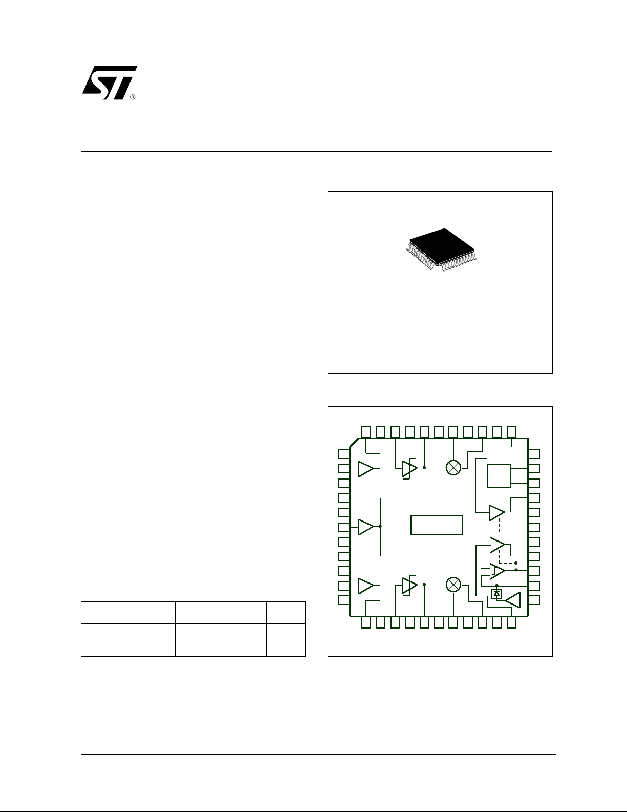
PACKAGE
F
TQFP44
10 x 10 mm
PIN CONNECTION (top view)
424344
424344
1
1
2
2
3
3
4
4
5
5
LNA
LNA
6
6
7
7
8
8
9
9
amp.
amp.
10
10
11
11
12 13 14 15 16 17 18 19 20 21 22
12 13 14 15 16 17 18 19 20 21 22
limiteramp.
limiteramp.
limiter
limiter
FM demodulator
FM demodulator
RX2
RX2
TSH511
TSH511
RX1
RX1
FM demodulator
FM demodulator
36
36
Vref
Vref
Standby
Standby
SQUELCH
SQUELCH
3435
3435
33
33
32
32
31
31
30
30
29
29
28
28
27
27
26
26
25
25
24
24
23
23
3738394041
3738394041
Audio
Audio
buffers
buffers
December 2002
1/18

TSH511
ABSOLUTE MAXIMUM RATINGS
Symbol Parameter Value Unit
Vcc
Supply voltage
Toper Operating free air temperature range -40 to +85 °C
Tstg Storage temperature -65 to +150 °C
Tj Maximum junction temperature 150 °C
Rthjc Thermal resistance juncti on to case 14 °C/W
ESD
except
for pin 6
HBM: Human Body Model
CDM: Charged Device Model
MM: Machine Model
HBM: Human Body Model
ESD
only
for pin 6
CDM: Charged Device Model
MM: Machine Model
Latch-up
1. All voltages values, except differential vol tage, are wit h respect to network gr ound terminal
2. ElectroS tatic Disch arge pulse (E SD pulse) sim ul ating a human body discharge of 10 0 pF through 1.5k
3. Discharge to Ground of a device that has been previously charged.
4. ElectroS tatic Disch arge pulse (E SD pulse) approximati ng a pulse of a ma chine or mec hanical equi pment.
5. Corporate ST Microelectr oni cs proced ure number 0018695
Class
5)
1)
2)
3)
4)
7V
2
1.5
0.2
1
1
0.1
A
Ω
kV
kV
OPERATING CONDITIONS
Symbol Parameter Value Unit
Vcc Supply voltage 2.3 to 5.5 V
f
audio
f
carrier
BLOC DIAGRAM
Audio frequency range 20 to 20,000 Hz
Carrier frequency range 0.4 to 11 MHz
BUF-IN2
MIX-OUT2
MIX-OUT2
Standby
Standby
GND
GND
3435363738
3435363738
SQUELCH
SQUELCH
BUF-IN2
GND
GND
33
33
32
32
SBY1
SBY1
SBY2
SBY2
31
31
30
30
BUF-OUT2
BUF-OUT2
29
29
VCC
VCC
28
28
DEC-OUT
DEC-OUT
27
27
GND
GND
26
26
BUF-OUT1
BUF-OUT1
25
25
MUTE-OUT
MUTE-OUT
24
24
MUTE-INT
MUTE-INT
23
23
MUTE-IN
MUTE-IN
GND
GND
AMP-I N2
AMP-I N2
VCC
VCC
LNA-OUT2
LNA-OUT2
VCC
VCC
LNA-IN
LNA-IN
GND
GND
LNA-OUT1
LNA-OUT1
VCC
VCC
AMP-I N1
AMP-I N1
DEC-LNA
DEC-LNA
DEC-LIM2B
GND
GND
LIM-IN2
LIM-IN2
424344
424344
limiteramp.
limiteramp.
limiter
limiter
DEC-LIM2B
40
40
41
41
RX2
RX2
TSH511
TSH511
RX1
RX1
AMP-OUT2
AMP-OUT2
1
1
2
2
3
3
4
4
5
5
LNA
LNA
6
6
7
7
8
8
9
9
amp.
amp.
10
10
11
11
LIM-OUT2
LIM-OUT2
DEC-LIM2A
DEC-LIM2A
39
39
FM demodulator
FM demodulator
FM demodulator
FM demodulator
MIX-IN2
MIX-IN2
VCC
VCC
Audio
Audio
buffers
buffers
Vref
Vref
2/18
12 13 14 15 16 17 18 19 20 21 22
12 13 14 15 16 17 18 19 20 21 22
MIX-IN1
MIX-IN1
DEC-LIM1B
LIM-IN1
LIM-IN1
AMP-OUT1
GND
AMP-OUT1
GND
DEC-LIM1B
VCC
VCC
MIX-OUT1
GND
MIX-OUT1
DEC-LIM1
LIM-OUT1
DEC-LIM1
LIM-OUT1
GND
BUF-IN1
BUF-IN1
PIN DESCRIPTION
TSH511
Pin Pin name related to
1 GND - - GROUND
2 AMP-IN2 RX2 I Intermediate amplifier input
3 VCC - - SUPPLY VOLTAGE
4 LNA-OUT2 RX2 O Low Noise Amplifier output
5 VCC - - SUPPLY VOLTAGE
6 LNA-IN RX1 & RX2 I Low Noise Amplifier input
7 GND - - GROUND
8 LNA-OUT1 RX1 O Low Noise Amplifier output
9 VCC - - SUPPLY VOLTAGE
10 AMP-IN1 RX1 I Intermediate amplifier input
11 DEC-LNA RX1 & RX2 - Decoupling capacitor
12 AMP-OUT1 RX1 O Intermediate amplifier input
13 GND - - GROUND
14 LIM-IN1 RX1 I Limiter input
15 DEC-LIM1A RX1 - Decoupling capacitor
16 LIM-OUT1 RX1 O Limiter output
17 DEC-LIM1B RX1 - Decoupling capacitor
18 MIX-IN1 RX1 I Mixer input
19 VCC - - SUPPLY VOLTAGE
20 MIX-OUT1 RX1 O Mixer output (demodulated audio signal)
21 GND - - GROUND
22 BUF-IN1 RX1 I Audio buffer input
23 MUTE-IN RX1 & RX2 I Noise amplifier input (Squelch circuit)
24 MUTE-INT RX1 & RX2 - Capacitor connection of the noise rectifier
25 MUTE-OUT RX1 & RX2 O Capacitor connection (ramp generator to mute the audio)
26 BUF-OUT1 RX1 O Audio buffer output
27 GND - - GROUND
28 DEC-OUT RX1 & RX2 - Decoupling capacitor of Audio buffers
29 VCC - - SUPPLY VOLTAGE
30 BUF-OUT2 RX2 O Audio buffer output
31 SBY2 RX1 & RX2 I Standby 2
32 SBY1 RX1 & RX2 I Standby 1
33 GND - - GROUND
34 BUF-IN2 RX2 I Audio buffer input
35 GND - - GROUND
36 MIX-OUT2 RX2 O Mixer output
37 VCC - - SUPPLY VOLTAGE
38 MIX-IN2 RX2 I Mixer input
39 DEC-LIM2A RX2 - Decoupling capacitor
40 LIM-OUT2 RX2 O Limiter output
41 DEC-LIM2B RX2 - Decoupling capacitor
42 LIM-IN2 RX2 I Limiter input
43 GND - - GROUND
44 AMP-OUT2 RX2 O Intermediate amplifier output
1. pin direction: I = inp ut pin, O = output pi n, - = pi n to connect to supply or deco upl i ng capacitors or external compo nents
direction
1)
Pin description
3/18
TSH511
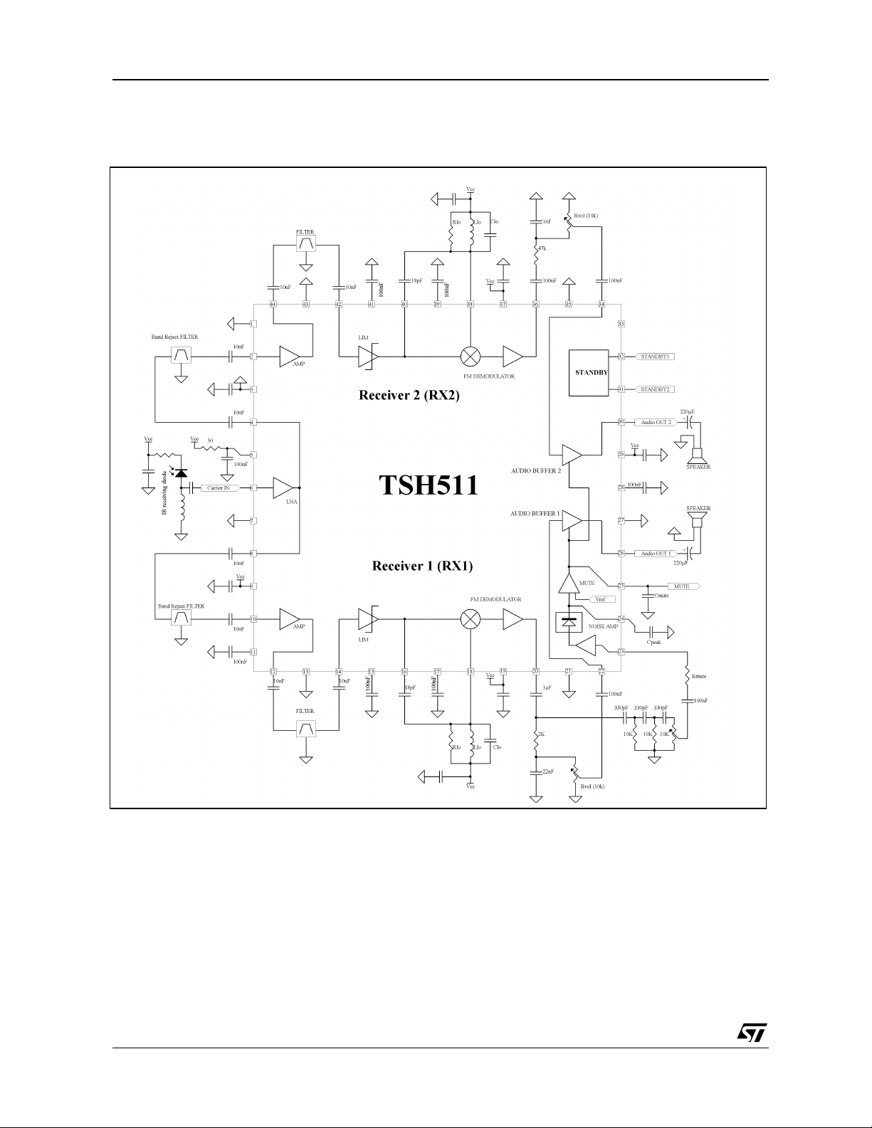
TYPICAL SCHEMATIC
Stereo infrared receiver
4/18
TSH511
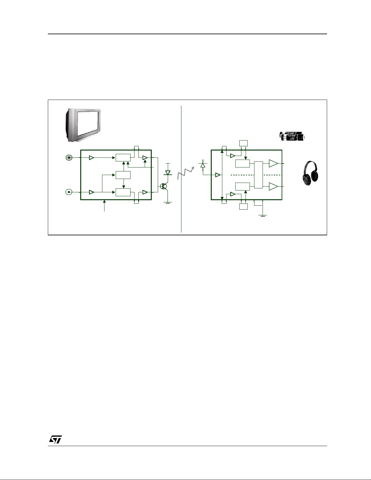
INFRARED STEREO HEADPHONE APPLICATION
The right side of the figure shows the block-diagram of an infrared stereo receiver using the TSH511. The
sensitive LNA directly connected to the photodiode does not require an external pre-amplifier. After filtering, the amplified signals are limited and demodulated with quadrature demodulators. The two integrated
audio buffers directly drive the stereo headphones. The aud io power reaches 2
The built-in squelch function fades-out the audio when the incoming infrared signal is low. The standby inputs SBY1 and SBY2 enable only one receiver for the mono applications.
x20mW in two 16Ω loads.
Right
Right
channel
channel
Line inputs
Line inputs
Left
Left
channel
channel
LNA + ALC
LNA + ALC
LNA + ALC
LNA + ALC
Power supply:
Power supply:
2.3 to 5.5V
2.3 to 5.5V
Icc < 20 mA stereo
Icc < 20 mA stereo
IR stereo HiFi transmitter
IR stereo HiFi transmitter
(Television)
(Television)
TSH512 TSH511
TSH512 TSH511
buffer2
TX2
TX2
VOX
VOX
TX1
TX1
buffer2
buffer1
buffer1
SBY
SBY
Vcc
Vcc
LED
LED
F
F
i
i
H
H
.
.
2
2
photodiode
photodiode
:
:
o
o
z
z
e
e
r
r
H
H
e
e
t
t
M
M
s
s
i
i
8
8
.
.
2
2
&
&
3
3
IR stereo HiFi receiver
IR stereo HiFi receiver
(Headphones)
(Headphones)
LNA
LNA
s
s
r
r
e
e
i
i
r
r
r
r
a
a
c
c
2.3 MHz
2.3 MHz
filter
filter
RX2
RX2
RX1
RX1
filter
filter
2.8 MHz
2.8 MHz
SQUELCH
SQUELCHSQUELCH
SBY1
SBY1
SBY2
SBY2
Vcc: 2.3 to 5.5V
Vcc: 2.3 to 5.5V
Current < 15 m A
Current < 15 m A
Audio
Audio
buffer2
buffer2
Audio
Audio
buffer1
buffer1
20 mW / 16 Ω
20 mW / 16 Ω
20 mW / 16 Ω
20 mW / 16 Ω
5/18

TSH511
MULTIMEDIA APPLICATION: HEADSET SIDE
The TSH511 recei ves the HiFi stereo sound f rom th e com pute r throu gh 2.3 and 2.8 MHz stereo infrared
carriers. The access pins to the RF amplifiers allow the use of a 1.7 M H z reject filter to c ancel the t ransmitted signal of the microphone. The wide supply range (2.3 to 5.5 V) allows battery operation.
TSH511 & 512 supply:
TSH511 & 512 supply:
TSH511 & 512 supply:
2.3 to 5.5V, 25 mA
2.3 to 5.5V, 25 mA
2.3 to 5.5V, 25 mA
Voice transmittedto the PC
Voice transmittedto the PC
Voice transmittedto the PC
TSH512
TSH512
TSH512
LNA + ALC
LNA + ALC
LNA + ALC
MIC. BIAS
MIC. BIAS
MIC. BIAS
MIC. BIAS
MIC. BIAS
MIC. BIAS
LNA + ALC
LNA + ALC
LNA + ALC
TX2
TX2
TX2
VOX
VOX
VOX
TX1
TX1
TX1
1.7 MHz
1.7 MHz
1.7 MHz
Band-pass
Band-pass
Band-pass
filter
filter
filter
buffer2
buffer2
buffer2
buffer1
buffer1
buffer1
SBY
SBY
SBY
HiFi stereofromthe PC:
HiFi stereofromthe PC:
HiFi stereofromthe PC:
2x 20 mW /16 Ω
2x 20 mW /16 Ω
2x 20 mW /16 Ω
Vcc
Vcc
Vcc
Vcc
Vcc
Vcc
LED
LED
LED
TSH511
TSH511
TSH511
Audio
Audio
Audio
buffer2
buffer2
buffer2
Audio
Audio
Audio
buffer1
buffer1
buffer1
1.7 MHz
1.7 MHz
1.7 MHz
reject
reject
reject
filter
filter
filter
RX2
RX2
RX2
SQUELCH
SQUELCH
SQUELCH
RX1
RX1
RX1
SBY1
SBY2
SBY1
SBY2
SBY1
SBY2
filter
filter
filter
1.7 MHz
1.7 MHz
1.7 MHz
reject
reject
reject
Microphone Tx:
Microphone Tx:
Microphone Tx:
1.7 MHz
1.7 MHz
1.7 MHz
carrier
carrier
carrier
2.3 MHz
2.3 MHz
2.3 MHz
Band-pass
Band-pass
Band-pass
filter
filter
filter
filter
filter
filter
2.8 MHz
2.8 MHz
2.8 MHz
Band-pass
Band-pass
Band-pass
LNA
LNA
LNA
Stereo Rx:
Stereo Rx:
Stereo Rx:
2.3 & 2.8 MHz
2.3 & 2.8 MHz
2.3 & 2.8 MHz
photodiode
photodiode
photodiode
MULTIMEDIA APPLICATION: COMPUTER SIDE
In multimedia application, the TSH511 receives the voice of the user through the 1.7 MHz infrared carrier.
The standby pins can disable the unused receiver and audio amplifier to reduce the supply current.
TSH511 & 512 supply:
TSH511 & 512 supply:
2.3 to 5.5V, 24 mA
2.3 to 5.5V, 24 mA
Voice from the headset microphoneHiFi stereo
mono Rx:
mono Rx:
1.7 MHz
1.7 MHz
HiFi stereo Tx:
HiFi stereo Tx:
2.3 & 2.8 MHz
2.3 & 2.8 MHz
LED
LED
buffer2
buffer2
SBY
SBY
buffer1
buffer1
TX2
TX2
VOX
VOX
TX1
TX1
TSH512
TSH512
LNA + ALC
LNA + ALC
LNA + ALC
LNA + ALC
photodiode
photodiode
Voice from the headset microphoneHiFi stereo
LNA
LNA
RX2
RX2
RX1
RX1
filter
filter
1.7 MHz
1.7 MHz
Band-pass
Band-pass
TSH511
TSH511
SQUELCH
SQUELCHSQUELCH
SBY2
SBY2
SBY1
SBY1
Vcc
Vcc
Audio
Audio
buffer2
buffer2
Audio
Audio
buffer 1
buffer 1
6/18
 Loading...