

SGS Thomson Microelectronics TSH151IN, TSH151ID, TSH151I, TSH151C Datasheet
TSH151
WIDE BANDWIDTHAND MOS INPUTS
SINGLE OPERATIONALAMPLIFIER
June 1998
ORDERCODES
Part
Number
Temperature
Range
Package
ND
TSH151C 0
o
C, 70oC ••
TSH151I -40
o
C, 125oC ••
151-01.TBL
1
2
3
4
8
6
5
7
Inverting Input
Non-invertingInput
Output
Offset Null 2Offset Null 1
N.C.
V
CC
V
CC
+
151-01.EPS
PINCONNECTIONS (top view)
.LOW DISTORTION
.GAIN BANDWIDTH PRODUCT : 150MHz
.UNITY GAIN STABLE
.SLEW RATE : 200V/µs
.VERY FASTSETTLING TIME : 70ns (0.1%)
.VERY HIGH INPUT IMPEDANCE
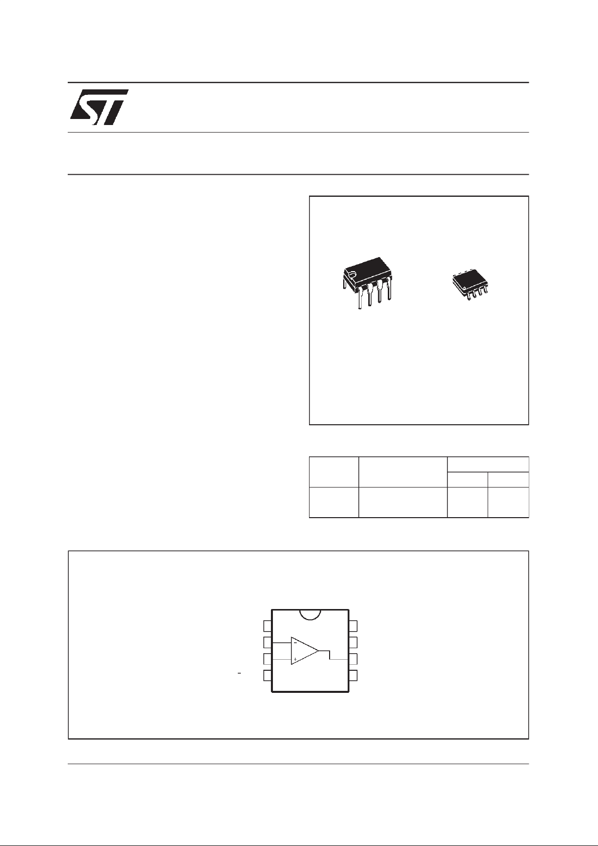
D
SO8
(Plastic Micropackage)
N
DIP8
(Plastic Package)
DESCRIPTION:
The TSH151is a widebandmonolithic operational
amplifier,internallycompensatedforunity-gainstability.
The TSH151features extremely high input impedance (typically greater than 10
12
Ω) allowing direct
interfacingwith high impedance sources.
Low distortion, wide bandwidth and high linearity
make this amplifiersuitableforRF and video applications. Short circuit protection is provided by an
internal current-limiting circuit.
The TSH151 has internal electrostatic discharge
(ESD)protection circuits andfulfillsMILSTD883CClass2.
1/7
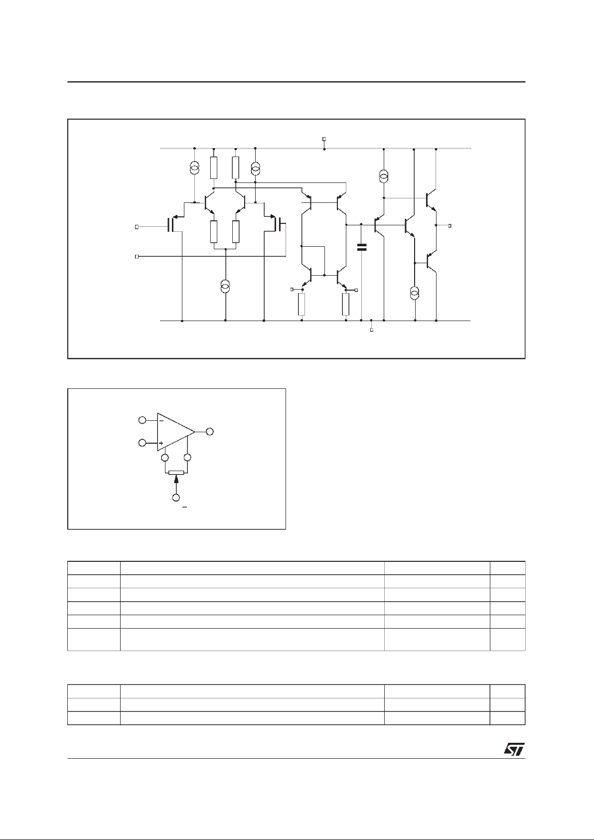
3
non inverting
input
2
inverting
input
1
8
Offset N1
Offset N2
7V
CC
+
C
c
6
output
Internal
V
CC
-
4
V
ref
151-02.EPS
SCHEMATICDIAGRAM
ABSOLUTEMAXIMUMRATINGS
Symbol Parameter Value Unit
V
CC
Supply Voltage ±7V
V
id
Differential Input Voltage ±5V
V
i
Input Voltage Range ±5V
I
in
Current On Offset Null Pins ±20 mA
T
oper
Operating Free-Air Temperature Range TSH151C
TSH151I
0oC, 70oC
-40
o
C, 15oC
o
C
151-02.TBL
N1
N2
TSH151
100k
Ω
V
CC
151-03.EPS
INPUT OFFSET VOLTAGENULL CIRCUIT
OPERATINGCONDITIONS
Symbol Parameter Value Unit
V
CC
Supply Voltage ±3to±6V
V
ic
Common Mode Input VoltageRange V
CC
-
to V
CC
+
-3 V
151-03.TBL
TSH151
2/7

ELECTRICALCHARACTERISTICS
V
CC
= ± 5V, T
amb
=25oC (unlessotherwisespecified)
Symbol Parameter
TSH151C, I
Unit
Min. Typ. Max.
V
io
Input Offset Voltage
T
min
≤ T
amb
≤ T
max.
0.5 10
12
mV
DV
io
Input Offset Voltage Drift
T
min
≤ T
amb
≤ T
max.
10
µV/
o
C
I
ib
Input Bias Current 2 300 pA
I
io
Input Offset Current 2 200 pA
I
CC
Supply Current, no load
V
CC
= ± 5V
V
CC
= ± 3V
V
CC
= ±6V
T
min
≤ T
amb
≤ T
max.
VCC= ± 5V
23
21
25
30
28
40
32
mA
A
vd
Large Signal VoltageGain
V
o
= ±2.5V
R
L
= ∞
R
L
= 100Ω
R
L
=50Ω
800
300
200
1300
850
650
V/V
V
icm
Input Common Mode Voltage Range -5 to +2 -5.5 to +2.5 V
CMR Common Mode Rejection Ratio V
ic=Vicm min.
60 100 dB
SVR Supply VoltageRejection Ratio
V
CC
= ± 5V to ± 3V 50 70
dB
V
o
Output Voltage RL= 100Ω
R
L
=50Ω
T
min
≤ T
amb
≤ T
max.
RL= 100Ω
R
L
=50Ω
±3
±2.8
± 2.9
± 2.7
+3.5
-3.7
+3.3
-3.5
V
I
o
Output Short Circuit Current
V
id
= ±1V, Vo=0V ±50 ±100
mA
GBP Gain Bandwidth Product
A
VCL
= 100, RL= 100Ω,CL= 15pF,f = 7.5MHz 150
MHz
SR Slew Rate
V
in
= ± 2V,A
VCL
=1,RL= 100Ω,CL= 15pF 100 200
V/µs
e
n
Equivalent Input VoltageNoise
R
S
=50Ω
fo = 1kHz
fo = 10kHz
fo = 100kHz
fo = 1MHz
20
18.2
18.1
18.2
nV
√Hz
K
ov
Overshoot
V
in
= ± 2V,A
VCL
=1,RL= 100Ω,CL= 15pF 10
%
t
s
Settling Time 0.1% - (note1)
V
in
= ± 1V,A
VCL
=-1 70
ns
t
r,tf
Rise and Fall Time - (note1)
V
in
= ±100mV,A
VCL
=2 5
ns
t
d
Delay Time - (note 1)
V
in
= ±100mV,A
VCL
=2 4
ns
∅m Phase Margin
A
VM
=1,RL= 100Ω, CL= 15pF 45
Degrees
THD Total Harmonic Distortion
A
VCL
= 10, f = 1KHz, Vo= ± 2.5V,no load 0.02
%
FPB Full Power Bandwidth - (note 2)
V
o
= 5Vpp, RL= 100Ω
V
o
= 2Vpp, RL= 100Ω
13
32
MHz
Note 1 : See test waveform figure
Note 2 : Full powerbandwidth =
SR
Π V
opp
151-04.TBL
TSH151
3/7
 Loading...