

SGS Thomson Microelectronics TSH113IDT, TSH113ID, TSH113, TSH112IDT, TSH112IPT Datasheet
...
TSH110-111-112-113-114
WIDE BAND, LOW NOISE OPERATIONAL AMPLIFIERS
■ LOW NOISE: 3nV/√Hz
■ LOW SUPPLY CURRENT: 3.2mA
■ 47mA OUTPUT CURRENT
■ BANDWIDTH: 100MHz
■ 5V to 12V SUPPLY VOLTAGE
■ SLEW-RAT E: 450V/µs
■ SPECIFIED F OR 100Ω Load
■ VERY LOW DISTORTION
■ TINY: SOT23-5, TSSOP and SO PACKAGES
DESCRIPTION
The singles TSH110 and TSH111, the dual
TSH112, the triple TSH113 and the quad TSH114
are current feedback operational amplifiers featur-
ing a very high slew rate of 450V /µs and a large
bandwidth of 100MHz, with only a 3.2mA quiescent supply current. The TSH111 and TSH113
feature a Standby function for each operator. This
function is a power down mode with a high outp ut
impedance.
These devices operate from
±2.5V to ±6V dual
supply voltage or from 5V to 12V single supply
voltage. They are able to drive a 100Ω load with a
swing of 9V minimum (for a 12V power supply).
The harmonic and intermodulation distortions of
these devices are very low, making this circuit a
good choice for applications requiring wide bandwidth with multiple carriers.
For board space and weight s aving, the TSH110
comes in miniature SOT23-5 package, the
TSH111 comes in SO8 and TS SOP8 packages,
the TSH112 comes in S O8 an d TSS OP 8 pack ages, the TSH113 and TSH114 comes in SO14 and
TSSOP14 packages.
APPLICATIONS
■ High End Video Drivers
■ Receiver for xDSL
■ A/D Converter Driver
■ High End Audio Applications
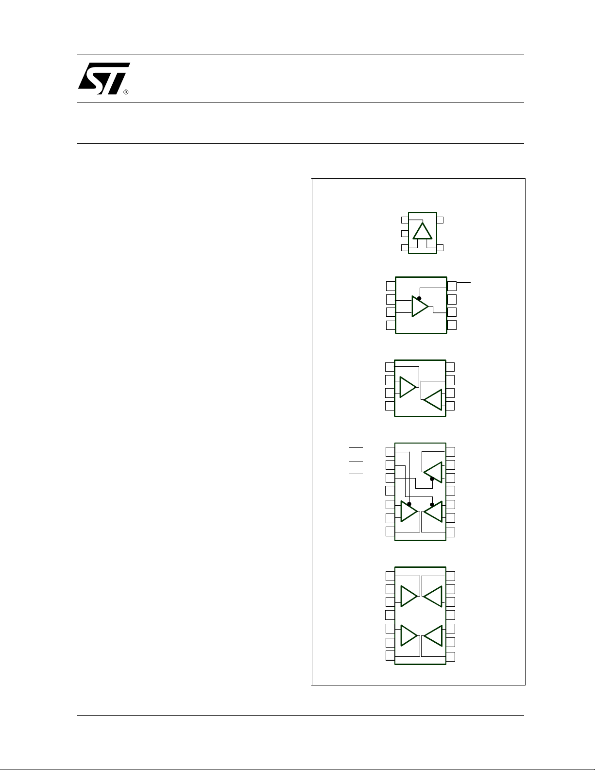
PIN CONNECTIONS (top view)
TSH110 : SOT23-5
TSH110 : SOT23-5
1
Output 1
Output
2
2
VCC -
VCC -
Non Inverting Input Inverting Input
Non Inverting Input Inverting Input
TSH111 : SO8/TSSOP8
TSH111 : SO8/TSSOP8
Inverting Input
Inverting Input
Non Inverting Input
Non Inverting Input
VCC -
VCC -
TSH112 : SO8/TSSOP8
TSH112 : SO8/TSSOP8
Output1
Output1
Inverting Input1 Output2
Inverting Input1 Output2
VCC -
VCC -
TSH113 : SO14/ TSSOP14
TSH113 : SO14/ TSSOP14
STANDBY1
STANDBY1
STANDBY2
STANDBY2
STANDBY3
STANDBY3
VCC + VCC -
VCC + VCC -
Non In v e rtin g Inpu t1
Non In v e rtin g Inpu t1
Inverting Input1
Inverting Input1
Output1
Output1
TSH114 : SO14/ TSSOP14
TSH114 : SO14/ TSSOP14
Output1
Output1
Inverting Input1
Inverting Input1
Non Inverting Input1
Non Inverting Input1
VCC +
VCC +
Non In v e rtin g Inpu t2
Non In v e rtin g Inpu t2
Inverting Input2
Inverting Input2
Output2
Output2
NC
NC
3
3
1
1
2
2
3
3
4
4
1
1
2
2
_
_
+
+
3
3
4
4
1
1
2
2
3
3
4
4
5
5
+
+
_
_
6
6
7
7
1
1
2
2
_
_
+
+
3
3
4
4
5
5
+
+
_
_
6
6
7
7
5
5
VCC +
VCC +
+ -
+ -
4
4
8
8
_
_
+
+
7
7
6
6
5
5
8
8
7
7
6Non Inverting Input1
6Non Inverting Input1
_
_
+
+
5
5
14
14
13
13
_
_
+
+
12
12
11
11
10
10
+
+
_
_
9
9
8
8
14
14
13
13
_
_
+
+
12
12
11
11
10
10
+
+
_
_
9
9
8
8
STANDBY
STANDBY
VCC +
VCC +
Output
Output
NC
NC
VCC +
VCC +
Inverting Input2
Inverting Input2
Non Inverting Input2
Non Inverting Input2
Output3
Output3
Inverting Input3
Inverting Input3
Non In v e rtin g Inpu t3
Non In v e rtin g Inpu t3
Non In v e rtin g Inpu t2
Non In v e rtin g Inpu t2
Inverting Input2
Inverting Input2
Output2
Output2
Output4
Output4
Inverting Input4
Inverting Input4
Non In v e rtin g Inpu t4
Non In v e rtin g Inpu t4
VCC -
VCC Non In v e rtin g Inpu t3
Non In v e rtin g Inpu t3
Inverting Input3
Inverting Input3
Output3
Output3
February 2002
1/19
TSH110-TSH111-TSH112-TSH113-TSH114
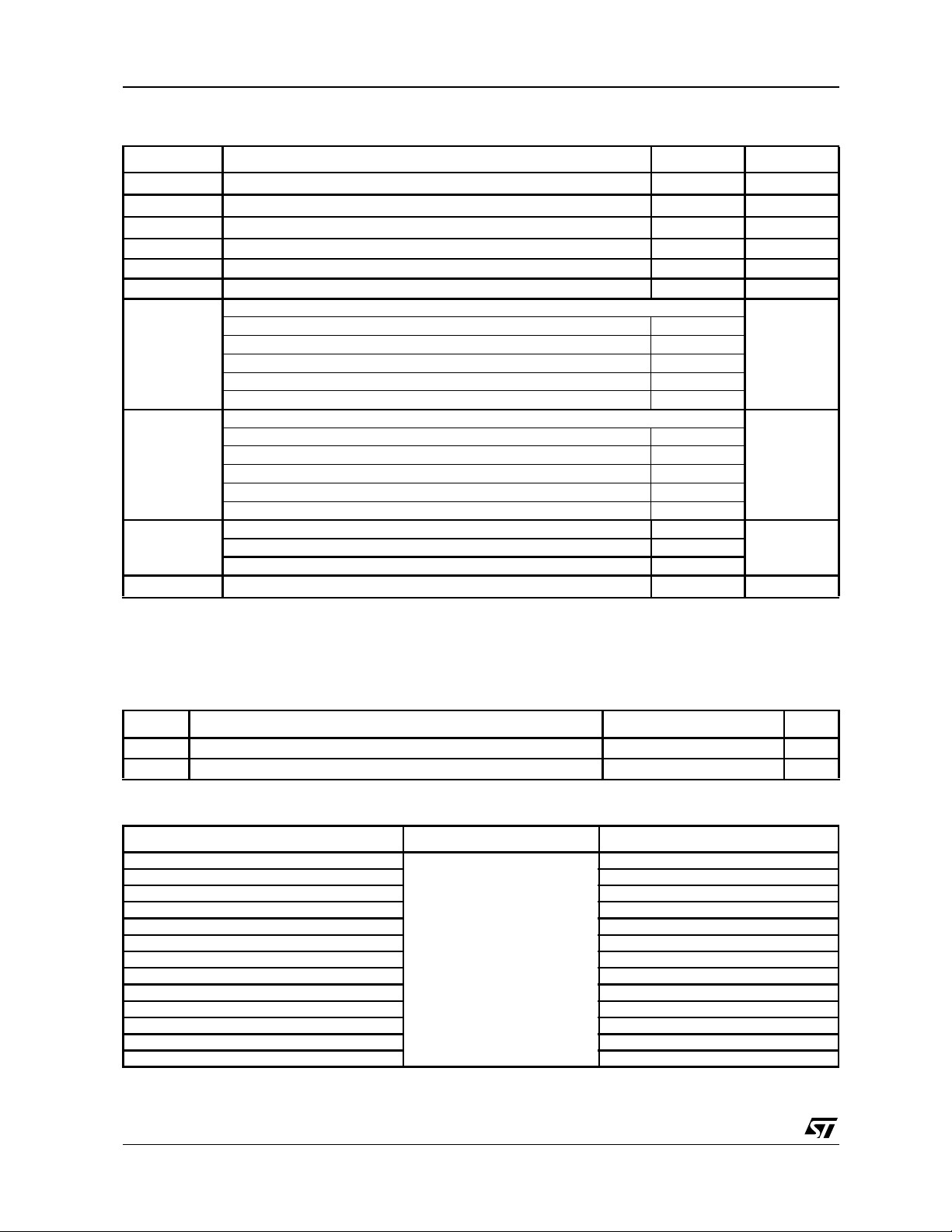
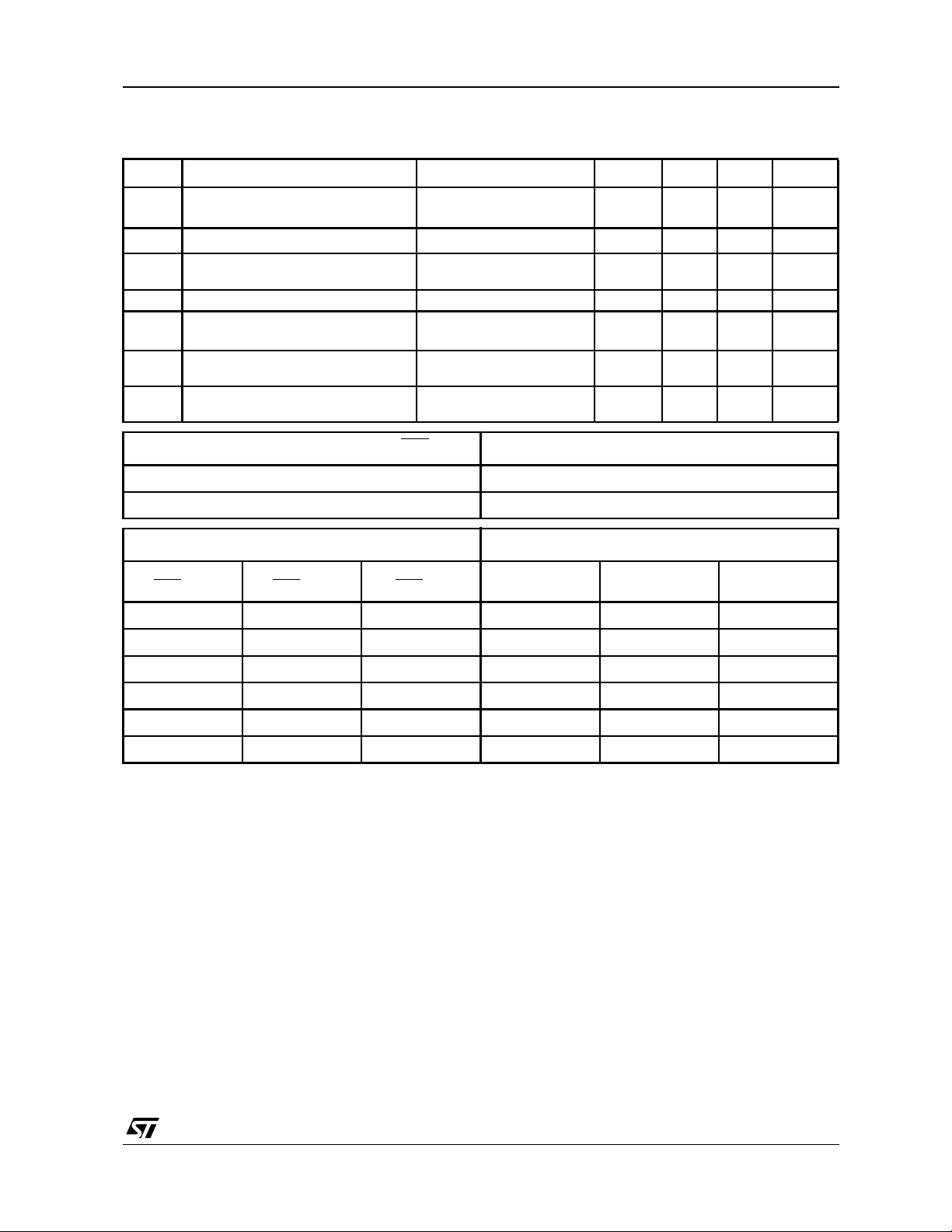
ABSOLUTE MAXIMUM RATINGS
Symbol Parameter Value Unit
V
CC
V
id
V
i
T
oper
T
stg
T
j
Supply Voltage
Differential Input Voltage
Input Voltage
Operating Free Air Temperature Range -40 to +85 °C
Storage Temperature -65 to +150 °C
Maximum Junction Temperature 150 °C
Thermal resistance junction to case
SOT23-5 80
R
thjc
SO8 28
SO14 22
TSSOP8 37
TSSOP14 32
Thermal resistance junction to ambiante area
SOT23-5 250
R
thja
SO8 157
SO14 125
TSSOP8 130
TSSOP14 110
Human Body Model 2.0
ESD
Charged Device Model 1.5
ouput short circuit duration
1. All voltages values, except differential voltage are with respect to network ground terminal
2. Differe ntial voltages are non-inverti ng input terminal wit h respect t o the inverting terminal
3. The magnit ude of input and output must never exc eed V
4. Short-circuits can cause excessive heating. Destructive dissipation can result.
1)
2)
3)
4)
+0.3 V
CC
14 V
±1 V
±6 V
°C/W
°C/W
kVMachine Model 0.2
OPERATING CONDITIONS
Symbol Parameter Value Unit
V
Vicm Common Mode Input Voltage Range
Supply Voltage 5 to 12 V
CC
V
+1.5 to V
CC-
CC+
-1.5
ORDER CODES
Type Temperature Package
TSH110ILT (code K302)
TSH111ID SO8
TSH111IDT SO8
TSH111IPT TSSOP8
TSH112ID SO8
TSH112IDT SO8
TSH112IPT TSSOP8
TSH113ID SO14
TSH113IDT SO14
TSH113IPT TSSOP14
TSH114ID SO14
TSH114IDT SO14
TSH114IPT TSSOP14
D = Small Outline Package (SO) - also available in Tape & Reel (DT)
P = Thin Shrink Small Outline Package (TSSOP) - only available in Tape & Reel (PT)
L = Tiny Package (SOT23-5) - only available in Tape & Reel (LT)
-40° to +85°C
2/19
SOT23-5
V

TSH110-TSH111-TSH112-TSH113-TSH114
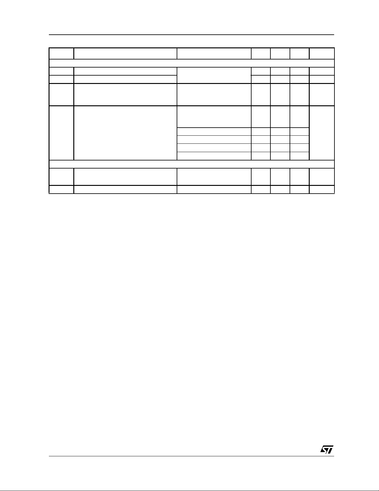
ELECTRICAL CHARACTERISTICS (pages 3 and 4)
Dual Supply Voltage, VCC= ±2.5Volts, R*fb = 680Ω, T
Symbol Parameter Test Condition Min. Typ. Max. Unit
DC PERFORMANCE
V
Input Offset Voltage
io
V
∆
CMR
SVR
PSR
Input Offset Voltage Drift vs. Temperature
io
I
Non Inverting Input Bias Current
ib+
I
Inverting Input Bias Current
ib-
R
Transimpedance
OL
I
Supply Current per Operator
CC
Common Mode Rejection Ratio
(
∆Vic/∆Vio)
Supply Voltage Rejection Ratio
∆VCC/∆Vio)
(
Power Supply Rejection Ratio
∆VCC/∆Vout)
(
DYNAMIC PERFORMANCE and OUTPUT CHARACTERISTICS
V
High Level Output Voltage
oh
V
Low Level Output Voltage
ol
| I
|
Output Sink current
sink
I
source
Output Source current
BW -3dB Bandwidth
SR Slew Rate
Tr Rise Time
Tf Fall Time 9ns
Ov Overshoot 16 %
St Settling Time @ 0.05% 60 ns
G Differential gain
∆
Differential phase 0.05 °
∆φ
T
T
T
T
T
T
T
R
T
T
Gain=1, Rload=3.9k
T
RL = 100
T
RL = 100Ω GND
T
RL = 100
T
RL = 100
T
T
Vout=1Vpk, Rfb*=820Ω//2pF
Load=100
A
A
Load=100
for 200mV step
A
Load=100
A
F=4.5MHz, V
= 25°C (unless otherwise specified)
amb
amb
min.
min.
amb
min.
amb
min.
=100
L
amb
min.
< T
< T
< T
< T
< T
Ω
amb
amb
amb
amb
amb
< T
< T
< T
< T
< T
max.
max.
max.
max.
max.
-1.5 0.3 2.0 mV
-10 1.4 13
-3 1.9 7
500 750 k
56 60 dB
70 80 dB
Ω
amb
min.
amb
< T
Ω
amb
< T
max.
1.4 2 V
Ω
< T
amb
< T
max.
min.
Ω
< T
< T
amb
amb
< T
< T
max.
max.
min.
min.
Ω
=+2
VCL
=+2, 2V step
VCL
Ω
=+2, Rfb*=820Ω//2pF
VCL
160 230 V/µs
Ω
=+2, RL=100
VCL
Ω
=1Vpeak
out
1mV
5
2.5
2.5
µ
V/°C
A
µ
A
µ
A
µ
A
µ
Ω
3.2 4 mA
3.5 mA
48 dB
1.9 V
-1.8 -1.3 V
-1.7 V
20 mA
18 mA
81 MHz
9ns
0.05 %
3/19
TSH110-TSH111-TSH112-TSH113-TSH114
Symbol Parameter Test Condition Min. Typ. Max. Unit
NOISE AND HARMONIC PERFORMANCE
en Equivalent Input Voltage Noise
in Equivalent Input Current Noise 8.5 pA/√Hz
THD Total Harmonic Distortion
Frequency : 1MHz
A
=+2, F=2MHz
VCL
R
=100
Ω
L
=2Vpeak
V
out
A
R
VCL
=100
L
=+2, V
=2Vpp
out
Ω
F1=1MHz, F2=1.1MHz
IM3 Third order inter modulation product
@900kHz 90
@1.2MHz 90
@3.1MHz 86
@3.2MHz 83
MATCHING CHARACTERISTICS
Gf Gain Flatness
F=(DC) to 6MHz
A
VCL
=+2, V
=2Vpp
out
Vo1/Vo2 Channel Separation F=1MHz to 10MHz 65 dB
(*) R
is the feedback resistance between the output and the inverting input of the amplifier.
fb
3 nV/√Hz
64.4 dB
0.1 dB
dBc
4/19
TSH110-TSH111-TSH112-TSH113-TSH114
ELECTRICAL CHARACTERISTICS (pages 5 and 6)
Dual Supply Voltage, VCC=±6Volts, R*fb = 680Ω, T
Symbol Parameter TestCondition Min. Typ. Max. Unit
DC PERFORMANCE
V
Input Offset Voltage
io
V
∆
CMR
SVR
PSR
DYNAMIC PERFORMANCE and OUTPUT CHARACTERISTICS
| I
I
source
Input Offset Voltage Drift vs Temperature
io
I
Non Inverting Input Bias Current
ib+
I
Inverting Input Bias Current
ib -
R
Transimpedance
OL
I
Supply Current per Operator
CC
Common Mode Rejection Ratio
(
∆Vic/∆Vio)
Supply Voltage Rejection Ratio
∆Vcc/∆Vio)
(
Power Supply Rejection Ratio
∆Vcc/∆Vout)
(
V
High Level Output Voltage
oh
V
Low Level Output Voltage
ol
|
Output Sink current
sink
Output Source current
Bw -3dB Bandwidth
SR Slew Rate
Tr Rise Time
Tf Fall Time 12.2 ns
Ov Overshoot 17 %
St Settling Time @ 0.05% 40 ns
G Differential gain
∆
Differential phase 0.05 °
∆φ
= 25°C (unless otherwise specified)
amb
T
amb
< T
T
min.
T
< T
min.
T
amb
< T
T
min.
T
amb
< T
T
min.
R
=100
L
T
amb
< T
T
min.
Ω
amb
amb
amb
amb
amb
< T
< T
< T
< T
< T
max.
max.
max.
max.
max.
-1.0 0.9 3.0 mV
-12 1 14
-4 3 10
600 900 k
58 63 dB
72 80 dB
Gain=1, Rload=3.9k
T
amb
RL = 100Ω
T
< T
amb
< T
min.
Ω
4.5 4.7 V
max.
RL = 100Ω
T
amb
RL = 100Ω
T
< T
amb
< T
max.
min.
RL = 100Ω
T
< T
< T
amb
amb
< T
< T
max.
max.
min.
T
min.
Vout=1Vpk, Rfb*=680Ω//2pF
Load=100
A
VCL
A
VCL
Load=100
Ω
=+2
=+2, 6V step
Ω
240 450 V/µs
for 200mV step
A
=+2, Rfb*=680Ω//2pF
VCL
Load=100
A
VCL
F=4.5MHz, V
Ω
=+2, RL=100Ω
=2Vpeak
out
1.3 mV
5
µ
1.7
3.4
45mA
4.1 mA
49 dB
4.6 V
-4.7 -4.3 V
-4.6 V
47 mA
46 mA
100 MHz
10.4 ns
0.05 %
V/°C
A
µ
A
µ
A
µ
A
µ
Ω
5/19

TSH110-TSH111-TSH112-TSH113-TSH114
Symbol Parameter TestCondition Min. Typ. Max. Unit
NOISE AND HARMONIC PERFORMANCE
en Equivalent Input Voltage Noise
in Equivalent Input Current Noise 8.6 pA/√Hz
THD Total Harmonic Distortion
Frequency : 1MHz
A
=+2, F=2MHz
VCL
R
=100Ω
L
=4Vpp
V
out
A
VCL
R
=100Ω
L
=+2, V
=4Vpp
out
F1=1MHz, F2=1.1MHz
IM3 Third order inter modulation product
@900kHz 82
@1.2MHz 84
@3.1MHz 77
@3.2MHz 73
MATCHING CHARACTERISTICS
Gf Gain Flatness
F=(DC) to 6MHz
A
VCL
=+2, V
=4Vpp
out
Vo1/Vo2 Channel Separation F=1MHz to 10MHz 65 dB
(*) R
is the feedback resistance between the output and the inverting input of the amplifier.
fb
3 nV/√Hz
67.7 dB
0.1 dB
dBc
6/19
TSH110-TSH111-TSH112-TSH113-TSH114
STANDBY MODE
T
= 25°C (unless otherwise specified), VCC=±6Volts
amb
Symbol Parameter Test Condition Min. Typ. Max. Unit
-
(V
Vl
V
high
I
CC SBY
I
sol
Z
out
T
T
Standby Low Level
ow
Standby High Level
Current Consumption per Operator in
Standby mode
-
V
CC
-
(V
+2) (V
CC
26 40
Input/Output Isolation F=1MHz -90 dB
Output Impedance (Rout // Cout)
Time from Standby Mode to Active
on
Mode
Time from Active Mode to Standby
off
Mode
R
out
C
out
Down to I
CC SBY
= 40µA
31
25
2
13
CC
+0.8)
CC
+
)
M
µ
pF
µ
µ
V
V
A
Ω
s
s
TSH111 STANDBY CONTROL pin 8 (SBY
V
low
V
high
TSH113 STANDBY CONTROL OPERATOR STATUS
pin 1
(SBY
V
V
high
x
x
OP1)
low
pin 2
(SBY OP2)
x x Standby x x
x x Active x x
V
low
V
high
xx
xx
) OPERATOR STATUS
Standby
Active
pin 3
(SBY OP)
OP1 OP1 OP3
x x Standby x
x Active x
V
low
V
high
x x Standby
x x Active
7/19

TSH110-TSH111-TSH112-TSH113-TSH114
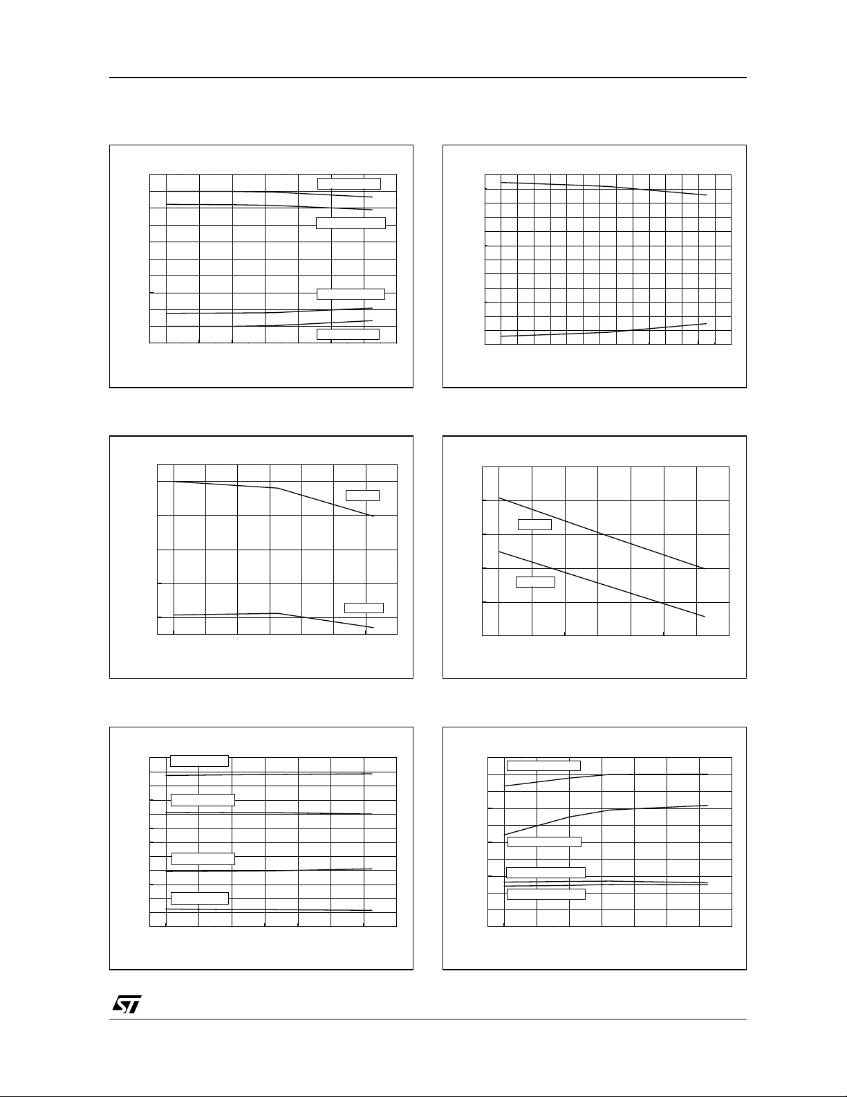
(fig.1) Closed Loop Gain vs. Frequency
AV=+1, Rfb=2.2kΩ, Cfb=2pF, RL=100Ω, Vin=100mVp
2
0
-2
V
-4
gain(dB)- A
-6
-8
-10
1 10 100
gain
phase
Vcc=±2.5V
Vcc=±6V
Frequency (MHz)
Vcc=±6V
Vcc=±2.5V
40
20
0
-20
-40
-60
-80
-100
-120
(fig.3) Closed Loop Gain vs. Frequency
AV=+2, Rfb=680Ω, Cfb=2pF, RL=100Ω, Vin=100mVp
40
6
4
V
2
0
gain(dB)- A
-2
-4
110100
gain
Vcc=±2.5V
phase
Vcc=±2.5V
Vcc=±6V
Freque nc y (MHz)
Vcc=±6V
20
0
-20
-40
-60
-80
-100
-120
(fig.2) Closed Loop Gain vs. Frequency
AV=-1, Rfb=2.2kΩ, Cfb=2pF, RL=100Ω, Vin=100mVp
2
0
-2
-4
Phase (°)
gain(dB)
-6
-8
-10
1 10 100
Vcc=±2.5V
Vcc=±6V
Frequency (MHz)
Vcc=±2.5V
Vcc=±6V
-140
-160
-180
-200
-220
-240
-260
-280
-300
Phase (°)
(fig.4) Closed Loop Gain vs. Frequency
AV=-2, Rfb=680kΩ, Cfb=2pF, RL=100Ω, Vin=100mVp
6
4
V
2
Phase (°)
0
gain(dB)- A
-2
-4
110100
gain
Vcc=±6V
phase
Vcc=±2.5V
Vcc=±6V
Freque nc y (M Hz)
Vcc=±2.5V
-140
-160
-180
-200
-220
-240
-260
-280
-300
Phase (°)
(fig.5) Closed Loop Gain vs. Frequency
AV=+10, Rfb=510Ω, RL=100Ω, Vin=30mVp
22
20
18
V
16
gain(dB)- A
14
12
10
1 10 100
8/19
gain
phase
Vcc=±2.5V
Vcc=±6V
Frequency (MHz)
Vcc=±6V
Vcc=±2.5V
40
20
0
-20
-40
-60
-80
-100
-120
(fig.6) Closed Loop Gain vs. Frequency
AV=-10, Rfb=510Ω, RL=100Ω, Vin=30mVp
22
20
18
V
16
Phase (°)
gain(dB)- A
14
12
10
110100
gain
phase
Vcc=±2.5V
Vcc=±6V
Frequency (MHz)
Vcc=±2.5V
Vcc=±6V
-140
-160
-180
-200
-220
-240
-260
-280
-300
Phase (°)

TSH110-TSH111-TSH112-TSH113-TSH114
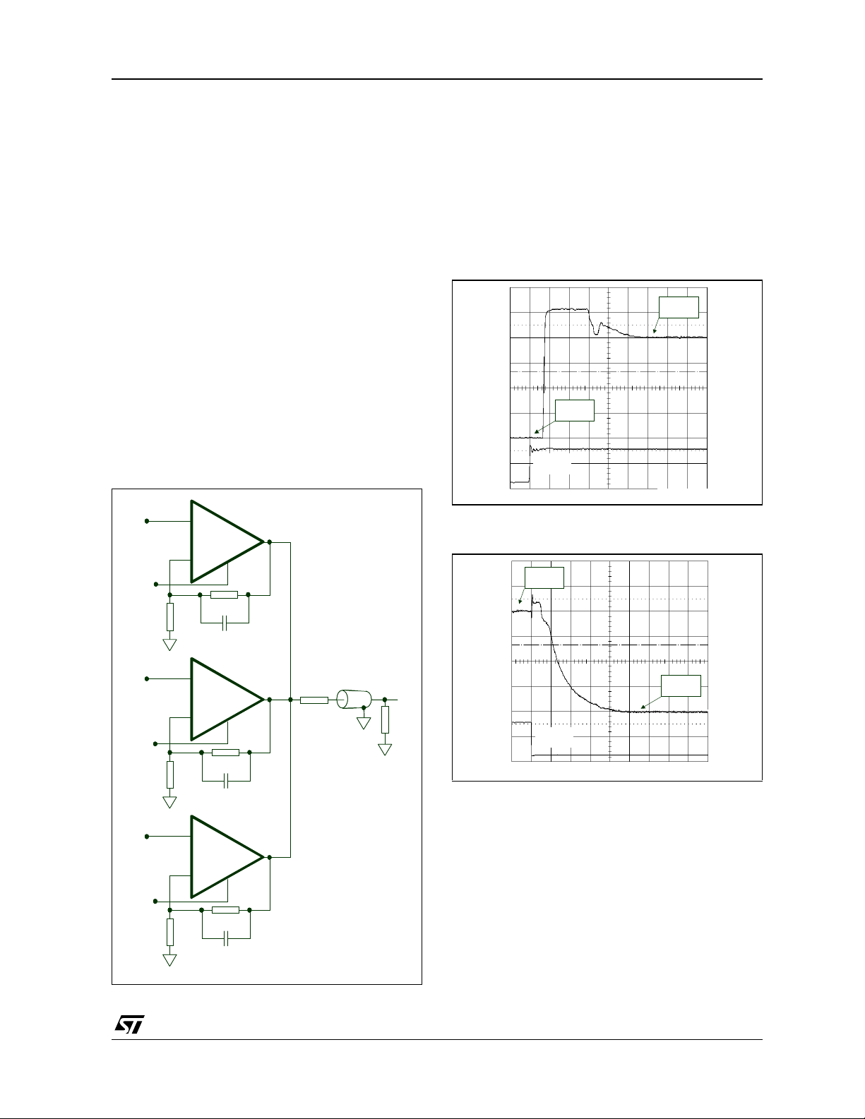
(fig.7): Positive Slew Rate
AV=+2, Rfb=680Ω, Cfb=2pF, RL=100Ω, Vcc=±6V
1V /div.
1V /div.
0V
0V
5ns /div.
5ns /div.
(fig.9): Positive Slew Rate
AV=+2, Rfb=680Ω, Cfb=2pF, RL=100Ω, Vcc=±2.5V
0.4V /div.
0.4V /div.
(fig.8): Negative Slew Rate
AV=+2, Rfb=680Ω, Cfb=2pF, RL=100Ω, Vcc=±6V
1V /div.
1V /div.
0V
0V
5ns /div.
5ns /div.
(fig.10): Negative Slew Rate
AV=+2, Rfb=680Ω, Cfb=2pF, RL=100Ω, Vcc=±2.5V
0.4V /div.
0.4V /div.
0V
0V
5ns /div.
5ns /div.
(fig.11): Input Voltage Noise Level
AV=+100, Rfb=1kΩ, Input+ connected to Gnd via 10
10
9
8
Hz)
√
7
6
5
4
3
Voltage Noise (nV/
2
1
0
100 1k 10k 100k 1M
Frequency (Hz)
Ω
0V
0V
5ns /div.
5ns /div.
(fig.12): V
Open loop, no load
(µV)
io
V
io vs. Power Supply
1000
900
800
700
600
500
400
300
200
56789101112
Vcc (V)
9/19

TSH110-TSH111-TSH112-TSH113-TSH114
(fig.13): Icc(-) vs. Power Supply
Open loop, no load
-3.3
-3.4
-3.5
-3.6
(mA)
cc(-)
I
-3.7
-3.8
-3.9
56789101112
Vcc (V)
(fig.15): I
Open loop, no load
ib(-) vs. Power Supply
3.2
3.0
2.8
2.6
(mA)
2.4
ib(-)
I
2.2
2.0
1.8
56789101112
Vcc (V)
(fig.14): I
cc(+) vs. Power Supply
Open loop, no load
3.9
3.8
3.7
3.6
(mA)
cc(+)
I
3.5
3.4
3.3
56789101112
(fig.16): I
ib(+) vs. Power Supply
Open loop, no load
1.0
0.8
0.6
(mA)
ib(+)
I
0.4
0.2
0.0
56789101112
Vcc (V)
Vcc (V)
(fig.17): V
ol vs. Po wer Supply
Open loop, RL=100
-2.0
-2.5
-3.0
-3.5
(V)
ol
V
-4.0
-4.5
-5.0
56789101112
10/19
Ω
(fig.18): V
Vcc (V)
Open loop, RL=100
(V)
oh
V
oh vs. Power Supply
Ω
5.0
4.5
4.0
3.5
3.0
2.5
2.0
56789101112
Vcc (V)
TSH110-TSH111-TSH112-TSH113-TSH114
(fig.19): Icc vs. Temperature
Open loop, no load
5
4
3
2
1
0
(mA)
cc
I
-1
-2
-3
-4
-5
-40 -20 0 20 40 60 80 100
(fig.21): R
OL vs. Temperature
Open loop, no load
1000
950
)
Ω
900
(k
OL
R
850
800
-40-20 0 20406080100
Temperature ( °C)
Temperature (°C)
Icc(+) for Vcc=±6V
Icc(+) for Vcc=±2.5V
Icc(-) for Vcc=±2.5V
Icc(-) for Vcc=±6V
Vcc=±6V
Vcc=±2.5V
(fig.20): I
cc (Standby) vs. Temperaure
Open loop, no load
30
20
10
A)
µ
0
Stand-By (
-10
cc
I
-20
-30
-40-200 20406080100
(fig.22): CMR
vs. Temperature
Open loop, no load
68
66
64
CMR (dB)
62
60
58
Vcc=±6V
Vcc=±2.5V
-40 -20 0 20 40 60 80 100
Temperature (°C)
Temperature (°C)
(fig.23): V
OH & VOL vs. Temperature
Open loop, RL=100
6
VOH for Vcc=±6V
5
4
VOH for Vcc=±2.5V
3
2
(V)
OL
1
0
and V
-1
OH
V
VOL for Vcc=±2.5V
-2
-3
VOL for Vcc=±6V
-4
-5
-6
-40 -20 0 20 40 60 80 100
Ω
Temperature ( °C)
(fig.24): Slew Rate vs. Temperature
AV=+2, RL=100
600
550
500
450
s)
µ
400
350
300
Slew Rate (V/
250
200
150
100
Ω
pos. SR for Vcc=±6V
neg. SR for Vcc=±6V
pos. SR for Vcc=±2.5V
neg. SR for Vcc=±2.5V
-40-200 20406080100
Temperature (°C)
11/19

TSH110-TSH111-TSH112-TSH113-TSH114
(fig.25): Group Delay
AV=+2, Rfb=680Ω, Cfb=2pF, RL=100Ω
8
7
6
5
4
Del ay Time (ns)
3
2
0.1 1 10 100
Frequency (MHz)
Vcc=±2.5V
Vcc=±6V
(fig.27): Frequency Response vs. Load
AV=+2, Rfb=680Ω, Cfb=2pF, VCC=±2.5V, (fig.2 9)
7
6
5
V
4
3
C=100pF Rs=12
Gain(dB) - A
2
1
0
1 10 100
C=1nF Rs=5
Frequency (MHz)
C=30pF Rs= 39
(fig.26): Gain Flatness
AV=+2, Rfb=680Ω, Cfb=2pF, RL=100Ω
6.30
6.25
6.20
6.15
6.10
6.05
Gain Flatness (dB)
6.00
5.95
5.90
1k 10k 100k 1M 10M 100M
Vcc=±2.5V
Vcc=±6V
Frequency (Hz)
(fig.28): Frequency Response vs. Load
AV=+2, Rfb=680Ω, Cfb=2pF, VCC=±6V, (fig.29)
7
6
5
V
4
3
C=100pF Rs=12
C=1nF Rs=6
Gain(dB) - A
2
1
0
110100
Frequency (MHz)
C=30pF Rs=30
(fig.29):
Capacitive Load Schematic.
measurements on (fig.27) and (fig.28)
+
+
TSH11x
TSH11x
Rs(Ω)
Rs(Ω)
RG
RG
680Ω
680Ω
_
_
R
R
fb, 680Ω
fb, 680Ω
Cfb 2pF
Cfb 2pF
12/19
1kΩ
1kΩ
OUT
OUT
C
C

TSH110-TSH111-TSH112-TSH113-TSH114
Interm od ul a tio n D ist o rt io n
A non-ideal output of the amplifier can be described by the following development :
V
=C0+C1(Vin)+C2(Vin)2+C3(Vin)3+...+Cn(Vin)
out
n
due to a non-linearity in the input-output amplitude
transfert. In the case of V
component, C
) is the fundamental, CnAn is
1(Vin
=Asinωt, CO is the DC
in
the amplitude of the harmonics.
A one-frequency or one-tone input signal contrib-
utes to a harmonic distortion. A two-tones input
signal contributes to a harmonic distortion and intermodulation product.
This intermodulation product or intermodulation
distortion of a two-tones input signal is the first
step of the amplifier stu dy for driving capab ility in
the case of a multitone signal.
In this case V
V
=
out
C
(Asinω1t+Bsinω2t)
O+C1
=Asinω1t+Bsinω2t, and :
in
+
(Asinω1t+Bsinω2t)2+C3(Asinω1t+Bsinω2t)
C
2
3
+
...C
V
out
C
n
)
n(Vin
=
(Asinω1t+Bsinω2t)
O+C1
+
(A2+B2)/2-(C2/2)(A2cos2ω1t+B2cos2ω2t)
C
2
+
2C
AB(cos(ω1-ω2)t-cos(ω1+ω2)t)
2
+
(3C
/4)
3
3
(A
sinω1t+B3sinω2t+2A2Bsinω2t+2B2Asinω1t)
+
(C
A3sin3ω1t+B3sin3ω2t)
3
+
(3C
A2B/2)(sin(2ω1-ω2)t-1/2sin(2ω1+ω2)t)
3
+
B2A/2)(sin(−ω1+2ω2)t-1/2sin(ω1+2ω2)t)
(3C
3
+
n(Vin
n
)
...C
In this expression, we can recognize the second
order intermodulation IM2 by the frequencies
(ω
) and (ω1+ω2) and the third order intermod-
1-ω2
ulation IM3 by the frequencies (2ω
+2ω2) and (ω1+2ω2).
(−ω
1
), (2ω1+ω2),
1-ω2
The following graphs show the IM3 of the amplifier
in two cases as a function of the output amplitude.
The two-tones input signal is achieved by the multisource generator Marconi 2026. E ach tone has
the same amplitude. The measurement is
achieved by the spectrum analyser HP 3585A.
Both instruments are phase locked to enhance
measurement precision.
(fig.30): 3
280kHz)
A
=+4, Rfb=680Ω, no Cfb, RL=100Ω, Vcc=±6V
V
IM3 (dBc)
-100
(fig.31): 3
1.1MHz)
=+2, Rfb=680Ω, Cfb=2pF, RL=100Ω, Vcc=±2.5V
A
V
IM3 (dBc)
rd
Order Intermodulation (180kHz &
-60
-65
-70
-75
-80
740kHz
380kHz
-85
-90
80kHz
-95
640kHz
012345
Outp ut Amplitu de ( V
rd
Order Intermodulation (1MHz &
-60
-65
-70
-75
3.2MHz
-80
3.1MHz
-85
1.2MHz
-90
900kHz
-95
-100
0.0 0.5 1.0 1.5 2.0
Output Amplitude (V
)
peak
)
peak
13/19

TSH110-TSH111-TSH112-TSH113-TSH114
+
_
-VCC
0.1µF
1µF
+VCC
1µF
0.1µF
TSH11x
+
_
-VCC
0.1µF
1µF
+VCC
1µF
0.1µF
TSH11x
Printed Circuit Board Layout Considerations
In this range of frequency, printed circuit board
parasitics can affect the closed-loop performance.
The implementation of a proper ground plane in
both sides of the PCB is mandatory to provide low
inductance and low resistance common return.
Most important for controlling the gain flatness
and the bandwidth are stray capac itances at the
output and inverting input. For minimizing the coupling, the space between signal lines and ground
plane will be increased. Connec tions of the feedback components must be as short as possible on
order to decrease the associated inductance
which affect high frequen cy gain errors. It is very
important to choose external components as small
as possible such as surface mounted devices,
SMD, in order to minimize the size of all the dc and
ac connections.
Power Supply Bypassing
A proper power suppl y bypass ing com es very im portant for optimizing the pe rformanc e in high frequency range. Bypass capac itors must be pl aced
as close as possible to the IC pins to improve high
frequency bypassing. A capacitor greater than
1µF is necessary to minim ize the distortion. For a
better quality bypas sing a capacitor of 0.1µF wil l
be added following the same condition of implementation. These bypass capacitors must be incorporated for the negative and the positive supplies.
(fig.32):
Circuit for power supply bypassing.
Nevertheless, the PCB layout has also an effect
on the crosstalk level. Capacitive coupling between signal wires, distance between critical signal nodes, power supply bypassing, are the most
significant points.
(fig.33):
AV=+2, Rfb=680Ω, Cfb=2pF, RL=100Ω, Vcc=±6V, ±2.5V
Crosstalk vs. Frequency.
0
-20
-40
-60
X-Talk (dB)
-80
-100
10k 100k 1M 10M 100M
Frequency (Hz)
Single Power Supply
The TSH11x operates from 12V down to 5V power
supplies. This is achieved with a d ual power sup-
ply of ±6V an d ±2.5V or a s ingle power s upply of
12V and 5V referenced to the grou nd. In t he cas e
of this asymmetrical supplying, a biasing is necessary to assume a positive output dynamic ran ge
between 0V and +Vcc supply rails. Considering
the values of V
OH and VOL, the am plifier will pro -
vide an ouput dynamic from +1.35V to 10.7 5V for
a 12V supplying, from 0.6V to 4.5V for a 5V supplying.
The following figure show the case of a 5V single
power supply configurati on.
Channel Separation or Crosstalk
The following figure show the crosstalk from an
amplifier to a second amplifier. This phenomenon,
accented in high frequ encies, is unavoidable and
intrinsic of the circuit.
14/19
(fig.34):
10µF
10µF
IN
IN
+5V
+5V
R1
R1
5kΩ
5kΩ
R1
R1
5kΩ
5kΩ
Circuit for +5V single supply.
+5V
+5V
+
+
Rin
Rin
1kΩ
1kΩ
+ 1µF
+ 1µF
10nF
10nF
+
+
G
G
R
R
680Ω
680Ω
CG
CG
_
_
TSH11x
TSH11x
R
R
fb, 680Ω
fb, 680Ω
Cfb
Cfb
2pF
2pF
100µF
100µF
50Ω
50Ω
OUT
OUT
50Ω
50Ω
TSH110-TSH111-TSH112-TSH113-TSH114
The amplifier must be biased with a mid supply
(nominaly +Vcc/2), in order to maintain the DC
component of the signa l at this val ue. Several options are possible to provide this bias supply (such
as a virtual ground using an operational amplifier),
or a two-resistance di vider which is the cheapest
solution. A high resistance value is required to limit the current consumption. On the other hand, the
current must be high enough to bias the non-inverting input of the amplifier. If we conside r this
bias current (5µA) as the 1% of the current
through the resistance divider (500µ A) to keep a
stable mid supply, two 5kΩ resistances can be
used.
The input provides a high pass filter with a break
frequency below 10Hz which is necessary to remove the original 0 volt DC component of the input
signal, and to hold it at 2.5V.
Video Multiplexing using the TSH113
(fig.35):
ple TSH113.
Circuit for switching 3 video signals with the tri-
+
IN1
IN1
ENABLE1
ENABLE1
RG
RG
680Ω
680Ω
+
_
_
TSH113
TSH113
R
R
fb, 680Ω
fb, 680Ω
Cfb, 2pF
Cfb, 2pF
Assuming a low l evel active onto the d isable p ins
(1,2,3) as described on pa ge 7 of the datasheet,
any operator can be disable/enable independent ly. The two disab led operators will be in sta ndby
mode featuring a high ouput impedance with a
high input/output isolation and a low quiescent
current.
(fig.36):
(fig.37):
Typical output response in standby mode on/off
Enabled
Enabled
Output
Output
0.4V /div.
0.4V /div.
Disabled
Disabled
Output
Output
+2.4V
+2.4V
Standby
Standby
Signal
Signal
-2.4V
-2.4V
100ns /div.
100ns /div.
Typical output response in standby mode off/on
Enabled
Enabled
Output
Output
0.4V /div.
0.4V /div.
IN2
IN2
ENABLE2
ENABLE2
RG
RG
680Ω
680Ω
IN3
IN3
ENABLE3
ENABLE3
RG
RG
680Ω
680Ω
+
+
_
_
+
+
_
_
TSH113
TSH113
fb, 680Ω
fb, 680Ω
R
R
Cfb, 2pF
Cfb, 2pF
TSH113
TSH113
fb, 680Ω
fb, 680Ω
R
R
Cfb, 2pF
Cfb, 2pF
75Ω
75Ω
cable
cable
75Ω
75Ω
Common
Common
OUT
OUT
75Ω
75Ω
+2.4V
+2.4V
Standby
Standby
Signal
Signal
-2.4V
-2.4V
Disabled
Disabled
Output
Output
10µs /div.
10µs /div.
15/19
TSH110-TSH111-TSH112-TSH113-TSH114
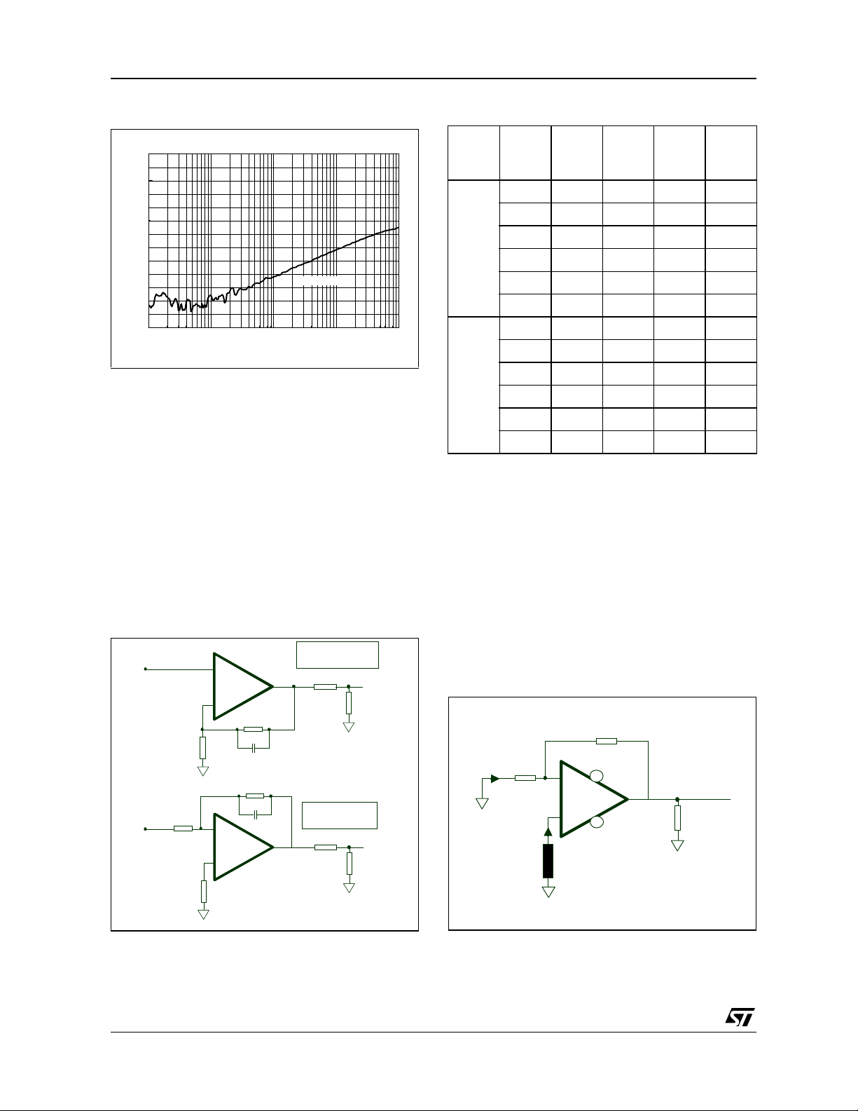
(fig.38):
Input / Output Isolation vs. Frequency..
0
-20
-40
-60
-80
-100
Input/output Iso lat ion (dB)
-120
0.01 0.1 1 10 100
Frequency (MHz)
Standby mode
Choice of the Feedback C ircuit
The TSH11x is a serie of current feedback
amplifiers. For a current feedback structure the
bandwidth depends on the value of the feedback
components and the value of supply voltage.
A good choice of thes e components is necessary
to achieve the gain flatness and the stability.
The following table shows the typical -3dB
bandwidth and 0.1dB bandwidth assuming
different gains and power supply on 100Ω load.
Please see also the Closed Loop Gain vs.
Frequency curves on page 8 of the datasheet.
(fig.39):
Non-inverting and Inverting Implementation.
Non- Inverting
Non-Inverting
Gain = 1+ R
Input
Input
Input
Input
Rin
Rin
RG
RG
+
+
_
_
Rfb
Rfb
Cfb
Cfb
Rfb
Rfb
Cfb
Cfb
_
_
+
+
Gain = 1+ R
Inverting
Inverting
Gain = -R
Gain = -R
49.9Ω
49.9Ω
49.9Ω
49.9Ω
fb / RG
fb / RG
Output
Output
fb / Rin
fb / Rin
Output
Output
50Ω
50Ω
50Ω
50Ω
.
(tab.1):
Closed-loop Gain and Feedback Components.
V
(V)
CC
Gain
R
(Ω)
Cfb
fb
(pF)
-3dB
Bw
(MHz)
0.1dB
Bw
(MHz)
+10 510 - 46 14
-10 510 - 42 13
+2 680 2 105 50
±6
-2 680 2 90 40
+1 2.2k 2 170 30
-1 2.2k 2 110 20
+10 510 - 37 13
-10 510 - 36 12
+2 680 2 93 25
±2.5
-2 680 2 86 30
+1 2.2k 2 130 50
-1 2.2k 2 100 18
Inverting Amplifier Biasin g
In this case a resistance (R on fig.40) is necessary
to achieve a good input biasing.
This resistance is calculated by assuming the
negative and posit ive input bias current . The aim
is to make the compensation of the offset bias
current which could affect the input offset voltage
and the output DC component.
Ass um ing Ib -, Ib + , R
the resistance R comes : R = R
(fig.40):
Compensation of the Input Bias Current.
Ib-
Ib-
Rin
Rin
Ib+
Ib+
in, Rfb and a zero volt o utp ut,
in // Rfb .
Rfb
Rfb
Vcc+
Vcc+
_
_
+
+
Vcc-
Vcc-
R
R
Output
Output
Load
Load
.
16/19
R
R
TSH110-TSH111-TSH112-TSH113-TSH114
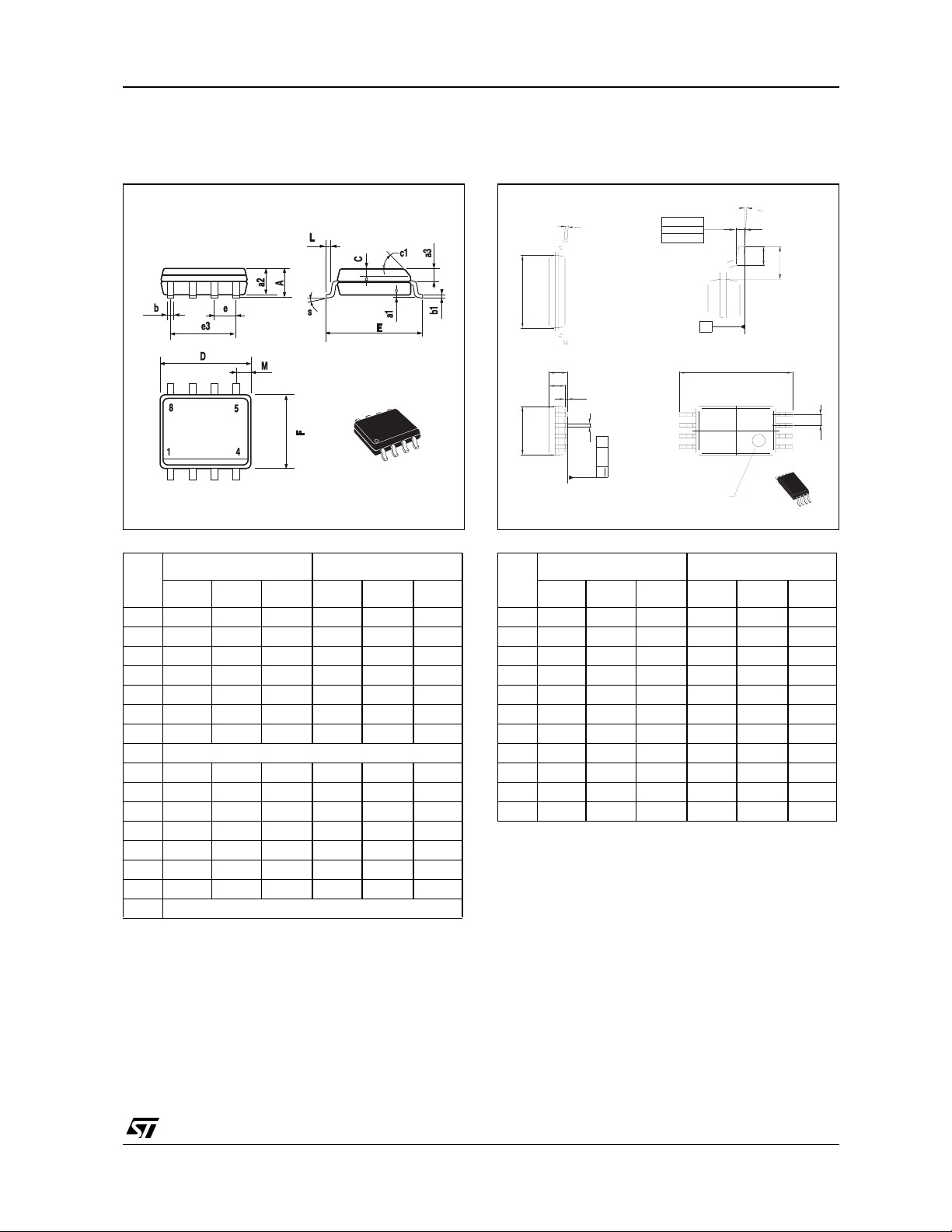
PACKAGE MECHANICAL DATA
8 PINS - PLASTIC MICROPACKAGE (SO)
Millimeters Inches
Dim.
Min. Typ. Max. Min. Typ. Max.
A 1.75 0.069
a1 0.1 0.25 0.004 0.010
a2 1.65 0.065
a3 0.65 0.85 0.026 0.033
b 0.35 0.48 0.014 0.019
b1 0.19 0.25 0.007 0.010
C 0.25 0.5 0.010 0.020
c1 45° (typ.)
D 4.8 5.0 0.189 0.197
E 5.8 6.2 0.228 0.244
e 1.27 0.050
e3 3.81 0.150
F 3.8 4.0 0.150 0.157
L 0.4 1.27 0.016 0.050
M 0.6 0.024
S 8° (max.)
PACKAGE MECHANICAL DATA
8 PINS - THIN SHRINK SMALL OUTL INE
PACKAGE (TSSOP)
c
E1
A2
A1
D
b
C
aaa
0,25 mm
.010 inch
GAGE PLANE
C
PLANE
SEATING
5
8
PIN 1 IDENTIFICATION
Millimeters Inches
Dim.
Min. Typ. Max. Min. Typ. Max.
A 1.20 0. 05
A1 0 .05 0.15 0.01 0.006
A2 0 .80 1.00 1.05 0.031 0.039 0.041
b 0.19 0.30 0.007 0.15
c 0.09 0.20 0.003 0.012
D 2.90 3.00 3.10 0 .114 0.118 0.122
E 6.40 0. 252
E1 4 .30 4.40 4.5 0 0.169 0. 173 0.177
e 0.65 0.025
k0° 8° 0° 8°
l 0.50 0.60 0.75 0.09 0.0236 0.030
k
L
L1
EA
14
e
17/19
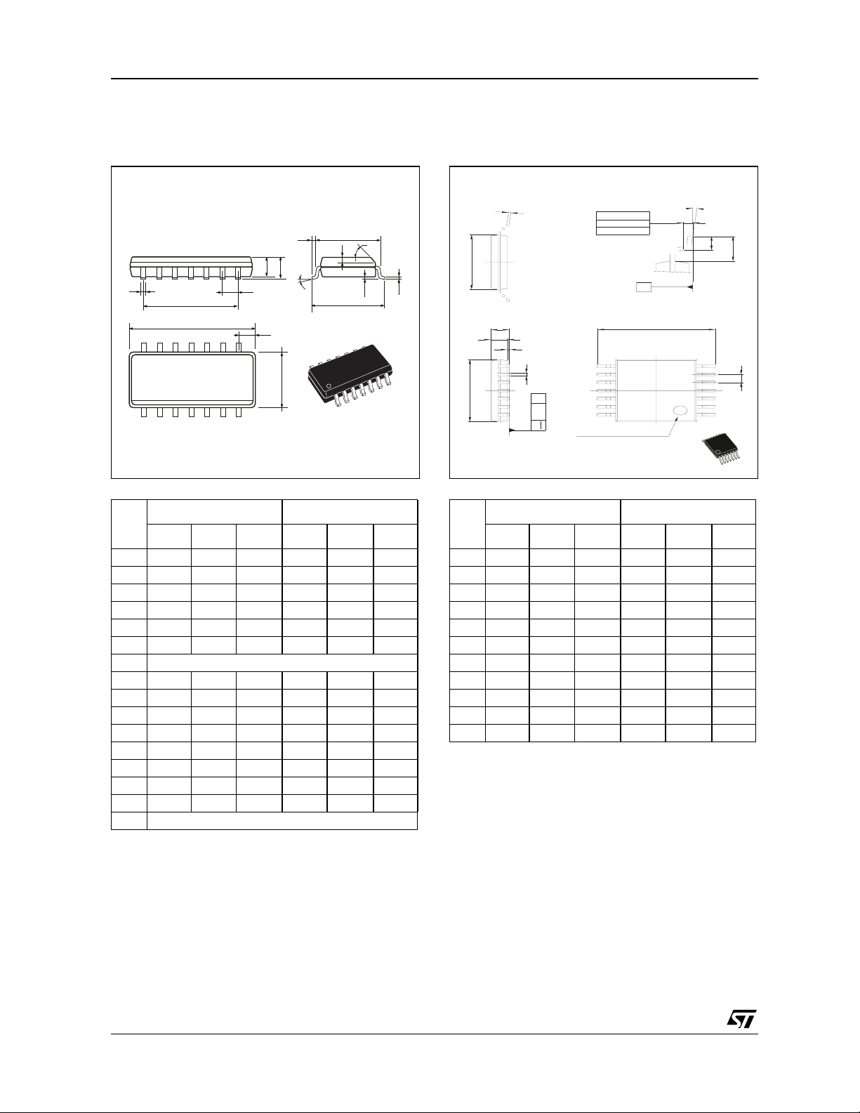
TSH110-TSH111-TSH112-TSH113-TSH114
PACKAGE MECHANICAL DATA
14 PINS - PLASTIC MICROPACKAGE (SO)
LG
A
a2
b
e3
14
1
e
D
M
8
7
s
F
Millimeters Inches
Dim.
Min. Typ. Max. Min. Typ. Max.
A 1.75 0.069
a1 0.1 0.2 0.004 0.008
a2 1.6 0.063
b 0.35 0.46 0.014 0.018
b1 0.19 0.25 0.007 0.010
C 0.5 0.020
c1 45° (typ.)
D (1) 8.55 8.75 0.336 0.344
E 5.8 6.2 0.228 0.244
e 1.27 0.050
e3 7.62 0.300
F (1) 3.8 4.0 0.150 0.157
G 4.6 5.3 0.181 0.208
L 0.5 1.27 0.020 0.050
M 0.68 0.027
S 8° (max.)
Note : (1) D and F do not include mold flash or protr usions - Mold f lash
or protrusions shall not exceed 0.15mm (.066 inc) ONLY FOR DATA
BOOK.
C
a1
E
c1
b1
PACKAGE MECHANICAL DATA
14 PINS - THIN SHRINK SMALL OUTLINE
PACKAGE (TSSOP)
c
E1
A
A2
A1
b
D
C
aaa
0,25 mm
.010 inch
GAGE PLANE
C
PLANE
SEATING
14
PIN 1 IDENTIFICATION
Millimeters Inches
Dim.
Min. Typ. Max. Min. Typ. Max.
A 1.20 0.05
A1 0.05 0.15 0.01 0.006
A2 0.80 1.00 1.05 0.031 0.039 0.041
b 0.19 0.30 0.007 0.15
c 0.09 0.20 0.003 0.012
D 4.90 5.00 5.10 0.192 0.196 0.20
E 6.40 0.252
E1 4.30 4.40 4.50 0.169 0.173 0.177
e 0.65 0.025
k0° 8° 0° 8°
l 0.50 0.60 0.75 0.09 0.0236 0.030
k
L
E
78
1
L1
e
18/19

TSH110-TSH111-TSH112-TSH113-TSH114
PACKAGE MECHANICAL DATA
2
5 PINS - TINY PACKAGE (SOT23)
A
E
D
E1
b
L
C
Millimeters Inches
Dim.
Min. Typ. Max. Min. Typ. Max.
A 0.90 1.20 1.45 0.035 0.047 0.057
A1 0 0.15 0.006
A2 0.90 1.05 1.30 0.035 0.041 0.051
B 0.35 0.40 0.50 0.014 0.016 0.020
C 0.09 0.15 0.20 0.004 0.006 0.008
D 2.80 2.90 3.00 0.110 0.114 0.118
D1 1.90 0.075
e 0.95 0.037
E 2.60 2.80 3.00 0.102 0.110 0.0118
F 1.50 1.60 1.75 0.059 0.063 0.069
L 0.10 0.5 0.60 0.004 0.014 0.024
K 0d 10d 0d 10d
A2
A1
Information furnished is bel ieved to be accurate and reliable. However, STMicroe lectronics assumes no responsibility for the
consequences of use of such information nor for any infringement of patents or other rights of third parties which may result from
its use. No li cense is granted by i mp lica tion or otherwise under a n y patent or patent rig hts of STMicroelectronics. Spec ific at ions
mentioned in this publication ar e subject to change without notice. This publication supersedes and replaces all information
previously supplied. S TMicroelectronics products are not authorized for use as critica l components in life suppo rt devices or
systems without express written approval of STMicroelectronics.
Australi a - Brazil - Canada - Chin a - F i nland - France - Germany - Hong Ko ng - India - Israel - Italy - Japan - Malaysia
Malta - Mor occo - Singapore - Spai n - Sweden - S wi t zerland - U n i t ed Kingdom - United Sta tes
© The ST logo is a registered trademark of STMicroelectronics
© 2002 STM icroelectronics - Printed in Italy - All Ri g h ts Reserv ed
STMicr o el ectronics G ROU P OF COMPANI E S
© http://www.st.com
19/19
 Loading...