

SGS Thomson Microelectronics TSH113IDT, TSH113ID, TSH113, TSH112IDT, TSH112IPT Datasheet
...
TSH110-111-112-113-114
WIDE BAND, LOW NOISE OPERATIONAL AMPLIFIERS
■ LOW NOISE: 3nV/√Hz
■ LOW SUPPLY CURRENT: 3.2mA
■ 47mA OUTPUT CURRENT
■ BANDWIDTH: 100MHz
■ 5V to 12V SUPPLY VOLTAGE
■ SLEW-RAT E: 450V/µs
■ SPECIFIED F OR 100Ω Load
■ VERY LOW DISTORTION
■ TINY: SOT23-5, TSSOP and SO PACKAGES
DESCRIPTION
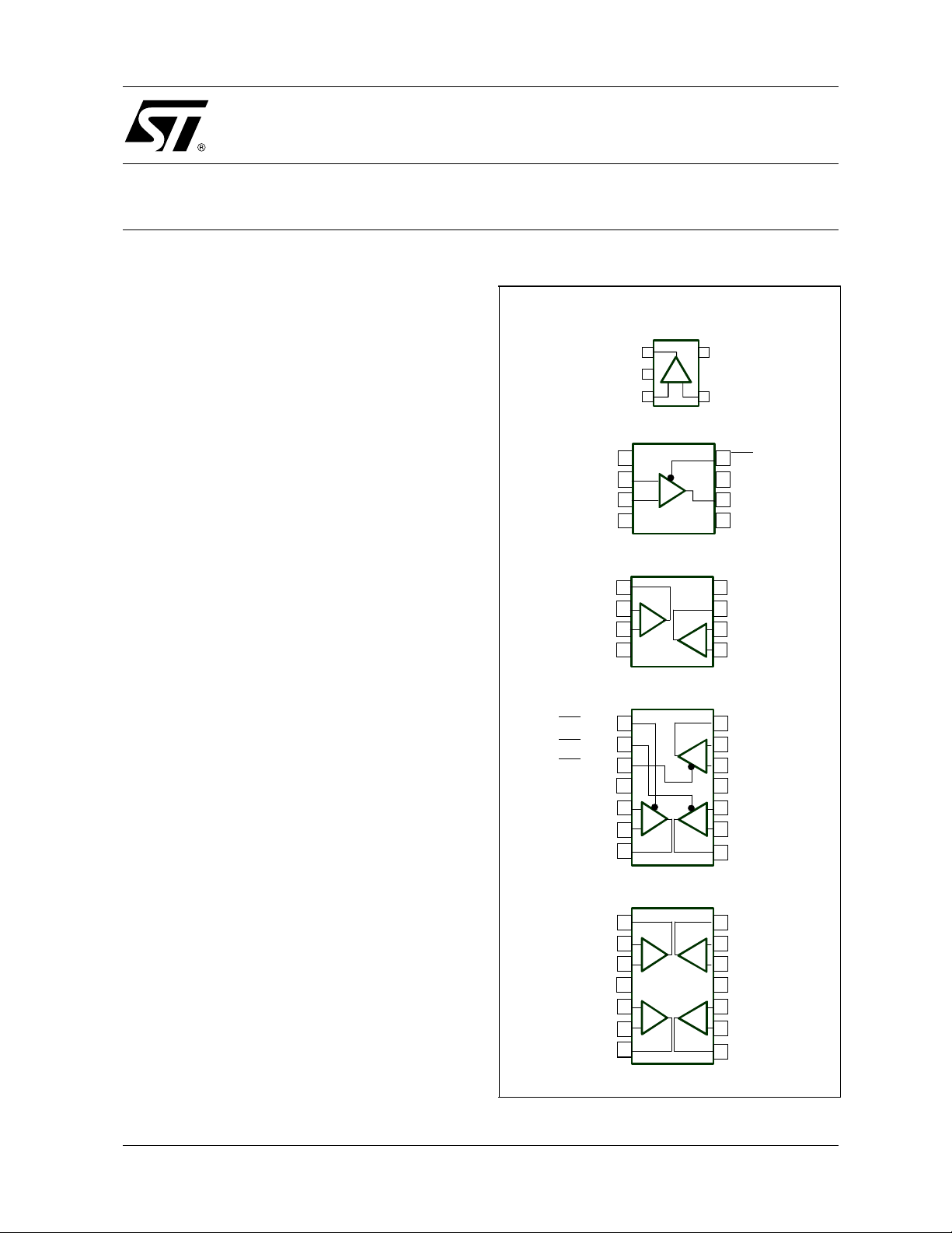
The singles TSH110 and TSH111, the dual
TSH112, the triple TSH113 and the quad TSH114
are current feedback operational amplifiers featur-
ing a very high slew rate of 450V /µs and a large
bandwidth of 100MHz, with only a 3.2mA quiescent supply current. The TSH111 and TSH113
feature a Standby function for each operator. This
function is a power down mode with a high outp ut
impedance.
These devices operate from
±2.5V to ±6V dual
supply voltage or from 5V to 12V single supply
voltage. They are able to drive a 100Ω load with a
swing of 9V minimum (for a 12V power supply).
The harmonic and intermodulation distortions of
these devices are very low, making this circuit a
good choice for applications requiring wide bandwidth with multiple carriers.
For board space and weight s aving, the TSH110
comes in miniature SOT23-5 package, the
TSH111 comes in SO8 and TS SOP8 packages,
the TSH112 comes in S O8 an d TSS OP 8 pack ages, the TSH113 and TSH114 comes in SO14 and
TSSOP14 packages.
APPLICATIONS
■ High End Video Drivers
■ Receiver for xDSL
■ A/D Converter Driver
■ High End Audio Applications
PIN CONNECTIONS (top view)
TSH110 : SOT23-5
TSH110 : SOT23-5
1
Output 1
Output
2
2
VCC -
VCC -
Non Inverting Input Inverting Input
Non Inverting Input Inverting Input
TSH111 : SO8/TSSOP8
TSH111 : SO8/TSSOP8
Inverting Input
Inverting Input
Non Inverting Input
Non Inverting Input
VCC -
VCC -
TSH112 : SO8/TSSOP8
TSH112 : SO8/TSSOP8
Output1
Output1
Inverting Input1 Output2
Inverting Input1 Output2
VCC -
VCC -
TSH113 : SO14/ TSSOP14
TSH113 : SO14/ TSSOP14
STANDBY1
STANDBY1
STANDBY2
STANDBY2
STANDBY3
STANDBY3
VCC + VCC -
VCC + VCC -
Non In v e rtin g Inpu t1
Non In v e rtin g Inpu t1
Inverting Input1
Inverting Input1
Output1
Output1
TSH114 : SO14/ TSSOP14
TSH114 : SO14/ TSSOP14
Output1
Output1
Inverting Input1
Inverting Input1
Non Inverting Input1
Non Inverting Input1
VCC +
VCC +
Non In v e rtin g Inpu t2
Non In v e rtin g Inpu t2
Inverting Input2
Inverting Input2
Output2
Output2
NC
NC
3
3
1
1
2
2
3
3
4
4
1
1
2
2
_
_
+
+
3
3
4
4
1
1
2
2
3
3
4
4
5
5
+
+
_
_
6
6
7
7
1
1
2
2
_
_
+
+
3
3
4
4
5
5
+
+
_
_
6
6
7
7
5
5
VCC +
VCC +
+ -
+ -
4
4
8
8
_
_
+
+
7
7
6
6
5
5
8
8
7
7
6Non Inverting Input1
6Non Inverting Input1
_
_
+
+
5
5
14
14
13
13
_
_
+
+
12
12
11
11
10
10
+
+
_
_
9
9
8
8
14
14
13
13
_
_
+
+
12
12
11
11
10
10
+
+
_
_
9
9
8
8
STANDBY
STANDBY
VCC +
VCC +
Output
Output
NC
NC
VCC +
VCC +
Inverting Input2
Inverting Input2
Non Inverting Input2
Non Inverting Input2
Output3
Output3
Inverting Input3
Inverting Input3
Non In v e rtin g Inpu t3
Non In v e rtin g Inpu t3
Non In v e rtin g Inpu t2
Non In v e rtin g Inpu t2
Inverting Input2
Inverting Input2
Output2
Output2
Output4
Output4
Inverting Input4
Inverting Input4
Non In v e rtin g Inpu t4
Non In v e rtin g Inpu t4
VCC -
VCC Non In v e rtin g Inpu t3
Non In v e rtin g Inpu t3
Inverting Input3
Inverting Input3
Output3
Output3
February 2002
1/19
TSH110-TSH111-TSH112-TSH113-TSH114
ABSOLUTE MAXIMUM RATINGS
Symbol Parameter Value Unit
V
CC
V
id
V
i
T
oper
T
stg
T
j
Supply Voltage
Differential Input Voltage
Input Voltage
Operating Free Air Temperature Range -40 to +85 °C
Storage Temperature -65 to +150 °C
Maximum Junction Temperature 150 °C
Thermal resistance junction to case
SOT23-5 80
R
thjc
SO8 28
SO14 22
TSSOP8 37
TSSOP14 32
Thermal resistance junction to ambiante area
SOT23-5 250
R
thja
SO8 157
SO14 125
TSSOP8 130
TSSOP14 110
Human Body Model 2.0
ESD
Charged Device Model 1.5
ouput short circuit duration
1. All voltages values, except differential voltage are with respect to network ground terminal
2. Differe ntial voltages are non-inverti ng input terminal wit h respect t o the inverting terminal
3. The magnit ude of input and output must never exc eed V
4. Short-circuits can cause excessive heating. Destructive dissipation can result.
1)
2)
3)
4)
+0.3 V
CC
14 V
±1 V
±6 V
°C/W
°C/W
kVMachine Model 0.2
OPERATING CONDITIONS
Symbol Parameter Value Unit
V
Vicm Common Mode Input Voltage Range
Supply Voltage 5 to 12 V
CC
V
+1.5 to V
CC-
CC+
-1.5
ORDER CODES
Type Temperature Package
TSH110ILT (code K302)
TSH111ID SO8
TSH111IDT SO8
TSH111IPT TSSOP8
TSH112ID SO8
TSH112IDT SO8
TSH112IPT TSSOP8
TSH113ID SO14
TSH113IDT SO14
TSH113IPT TSSOP14
TSH114ID SO14
TSH114IDT SO14
TSH114IPT TSSOP14
D = Small Outline Package (SO) - also available in Tape & Reel (DT)
P = Thin Shrink Small Outline Package (TSSOP) - only available in Tape & Reel (PT)
L = Tiny Package (SOT23-5) - only available in Tape & Reel (LT)
-40° to +85°C
2/19
SOT23-5
V

TSH110-TSH111-TSH112-TSH113-TSH114
ELECTRICAL CHARACTERISTICS (pages 3 and 4)
Dual Supply Voltage, VCC= ±2.5Volts, R*fb = 680Ω, T
Symbol Parameter Test Condition Min. Typ. Max. Unit
DC PERFORMANCE
V
Input Offset Voltage
io
V
∆
CMR
SVR
PSR
Input Offset Voltage Drift vs. Temperature
io
I
Non Inverting Input Bias Current
ib+
I
Inverting Input Bias Current
ib-
R
Transimpedance
OL
I
Supply Current per Operator
CC
Common Mode Rejection Ratio
(
∆Vic/∆Vio)
Supply Voltage Rejection Ratio
∆VCC/∆Vio)
(
Power Supply Rejection Ratio
∆VCC/∆Vout)
(
DYNAMIC PERFORMANCE and OUTPUT CHARACTERISTICS
V
High Level Output Voltage
oh
V
Low Level Output Voltage
ol
| I
|
Output Sink current
sink
I
source
Output Source current
BW -3dB Bandwidth
SR Slew Rate
Tr Rise Time
Tf Fall Time 9ns
Ov Overshoot 16 %
St Settling Time @ 0.05% 60 ns
G Differential gain
∆
Differential phase 0.05 °
∆φ
T
T
T
T
T
T
T
R
T
T
Gain=1, Rload=3.9k
T
RL = 100
T
RL = 100Ω GND
T
RL = 100
T
RL = 100
T
T
Vout=1Vpk, Rfb*=820Ω//2pF
Load=100
A
A
Load=100
for 200mV step
A
Load=100
A
F=4.5MHz, V
= 25°C (unless otherwise specified)
amb
amb
min.
min.
amb
min.
amb
min.
=100
L
amb
min.
< T
< T
< T
< T
< T
Ω
amb
amb
amb
amb
amb
< T
< T
< T
< T
< T
max.
max.
max.
max.
max.
-1.5 0.3 2.0 mV
-10 1.4 13
-3 1.9 7
500 750 k
56 60 dB
70 80 dB
Ω
amb
min.
amb
< T
Ω
amb
< T
max.
1.4 2 V
Ω
< T
amb
< T
max.
min.
Ω
< T
< T
amb
amb
< T
< T
max.
max.
min.
min.
Ω
=+2
VCL
=+2, 2V step
VCL
Ω
=+2, Rfb*=820Ω//2pF
VCL
160 230 V/µs
Ω
=+2, RL=100
VCL
Ω
=1Vpeak
out
1mV
5
2.5
2.5
µ
V/°C
A
µ
A
µ
A
µ
A
µ
Ω
3.2 4 mA
3.5 mA
48 dB
1.9 V
-1.8 -1.3 V
-1.7 V
20 mA
18 mA
81 MHz
9ns
0.05 %
3/19
TSH110-TSH111-TSH112-TSH113-TSH114
Symbol Parameter Test Condition Min. Typ. Max. Unit
NOISE AND HARMONIC PERFORMANCE
en Equivalent Input Voltage Noise
in Equivalent Input Current Noise 8.5 pA/√Hz
THD Total Harmonic Distortion
Frequency : 1MHz
A
=+2, F=2MHz
VCL
R
=100
Ω
L
=2Vpeak
V
out
A
R
VCL
=100
L
=+2, V
=2Vpp
out
Ω
F1=1MHz, F2=1.1MHz
IM3 Third order inter modulation product
@900kHz 90
@1.2MHz 90
@3.1MHz 86
@3.2MHz 83
MATCHING CHARACTERISTICS
Gf Gain Flatness
F=(DC) to 6MHz
A
VCL
=+2, V
=2Vpp
out
Vo1/Vo2 Channel Separation F=1MHz to 10MHz 65 dB
(*) R
is the feedback resistance between the output and the inverting input of the amplifier.
fb
3 nV/√Hz
64.4 dB
0.1 dB
dBc
4/19
TSH110-TSH111-TSH112-TSH113-TSH114
ELECTRICAL CHARACTERISTICS (pages 5 and 6)
Dual Supply Voltage, VCC=±6Volts, R*fb = 680Ω, T
Symbol Parameter TestCondition Min. Typ. Max. Unit
DC PERFORMANCE
V
Input Offset Voltage
io
V
∆
CMR
SVR
PSR
DYNAMIC PERFORMANCE and OUTPUT CHARACTERISTICS
| I
I
source
Input Offset Voltage Drift vs Temperature
io
I
Non Inverting Input Bias Current
ib+
I
Inverting Input Bias Current
ib -
R
Transimpedance
OL
I
Supply Current per Operator
CC
Common Mode Rejection Ratio
(
∆Vic/∆Vio)
Supply Voltage Rejection Ratio
∆Vcc/∆Vio)
(
Power Supply Rejection Ratio
∆Vcc/∆Vout)
(
V
High Level Output Voltage
oh
V
Low Level Output Voltage
ol
|
Output Sink current
sink
Output Source current
Bw -3dB Bandwidth
SR Slew Rate
Tr Rise Time
Tf Fall Time 12.2 ns
Ov Overshoot 17 %
St Settling Time @ 0.05% 40 ns
G Differential gain
∆
Differential phase 0.05 °
∆φ
= 25°C (unless otherwise specified)
amb
T
amb
< T
T
min.
T
< T
min.
T
amb
< T
T
min.
T
amb
< T
T
min.
R
=100
L
T
amb
< T
T
min.
Ω
amb
amb
amb
amb
amb
< T
< T
< T
< T
< T
max.
max.
max.
max.
max.
-1.0 0.9 3.0 mV
-12 1 14
-4 3 10
600 900 k
58 63 dB
72 80 dB
Gain=1, Rload=3.9k
T
amb
RL = 100Ω
T
< T
amb
< T
min.
Ω
4.5 4.7 V
max.
RL = 100Ω
T
amb
RL = 100Ω
T
< T
amb
< T
max.
min.
RL = 100Ω
T
< T
< T
amb
amb
< T
< T
max.
max.
min.
T
min.
Vout=1Vpk, Rfb*=680Ω//2pF
Load=100
A
VCL
A
VCL
Load=100
Ω
=+2
=+2, 6V step
Ω
240 450 V/µs
for 200mV step
A
=+2, Rfb*=680Ω//2pF
VCL
Load=100
A
VCL
F=4.5MHz, V
Ω
=+2, RL=100Ω
=2Vpeak
out
1.3 mV
5
µ
1.7
3.4
45mA
4.1 mA
49 dB
4.6 V
-4.7 -4.3 V
-4.6 V
47 mA
46 mA
100 MHz
10.4 ns
0.05 %
V/°C
A
µ
A
µ
A
µ
A
µ
Ω
5/19

TSH110-TSH111-TSH112-TSH113-TSH114
Symbol Parameter TestCondition Min. Typ. Max. Unit
NOISE AND HARMONIC PERFORMANCE
en Equivalent Input Voltage Noise
in Equivalent Input Current Noise 8.6 pA/√Hz
THD Total Harmonic Distortion
Frequency : 1MHz
A
=+2, F=2MHz
VCL
R
=100Ω
L
=4Vpp
V
out
A
VCL
R
=100Ω
L
=+2, V
=4Vpp
out
F1=1MHz, F2=1.1MHz
IM3 Third order inter modulation product
@900kHz 82
@1.2MHz 84
@3.1MHz 77
@3.2MHz 73
MATCHING CHARACTERISTICS
Gf Gain Flatness
F=(DC) to 6MHz
A
VCL
=+2, V
=4Vpp
out
Vo1/Vo2 Channel Separation F=1MHz to 10MHz 65 dB
(*) R
is the feedback resistance between the output and the inverting input of the amplifier.
fb
3 nV/√Hz
67.7 dB
0.1 dB
dBc
6/19
 Loading...