

TSH11
120MHz BANDWIDTH MOSINPUT
SINGLE OPERATIONAL AMPLIFIER
June 1998
ORDERCODES
Part
Number
Temperature
Range
Package
ND
TSH11I -40
o
C, 125oC ••
1
2
3
4
8
6
5
7
Inverting Input
Non-inverting Input
Output
Offset Null2Offset Null1
N.C.
V
CC
V
CC
+
PINCONNECTIONS (topview)
.VERY LOW INPUT CURRENT : 2pA typ
.GAIN BANDWIDTH PRODUCT : 120MHz
.UNITY GAIN STABLE
.SLEW RATE : 150V/µs
.STANDARDPIN OUT
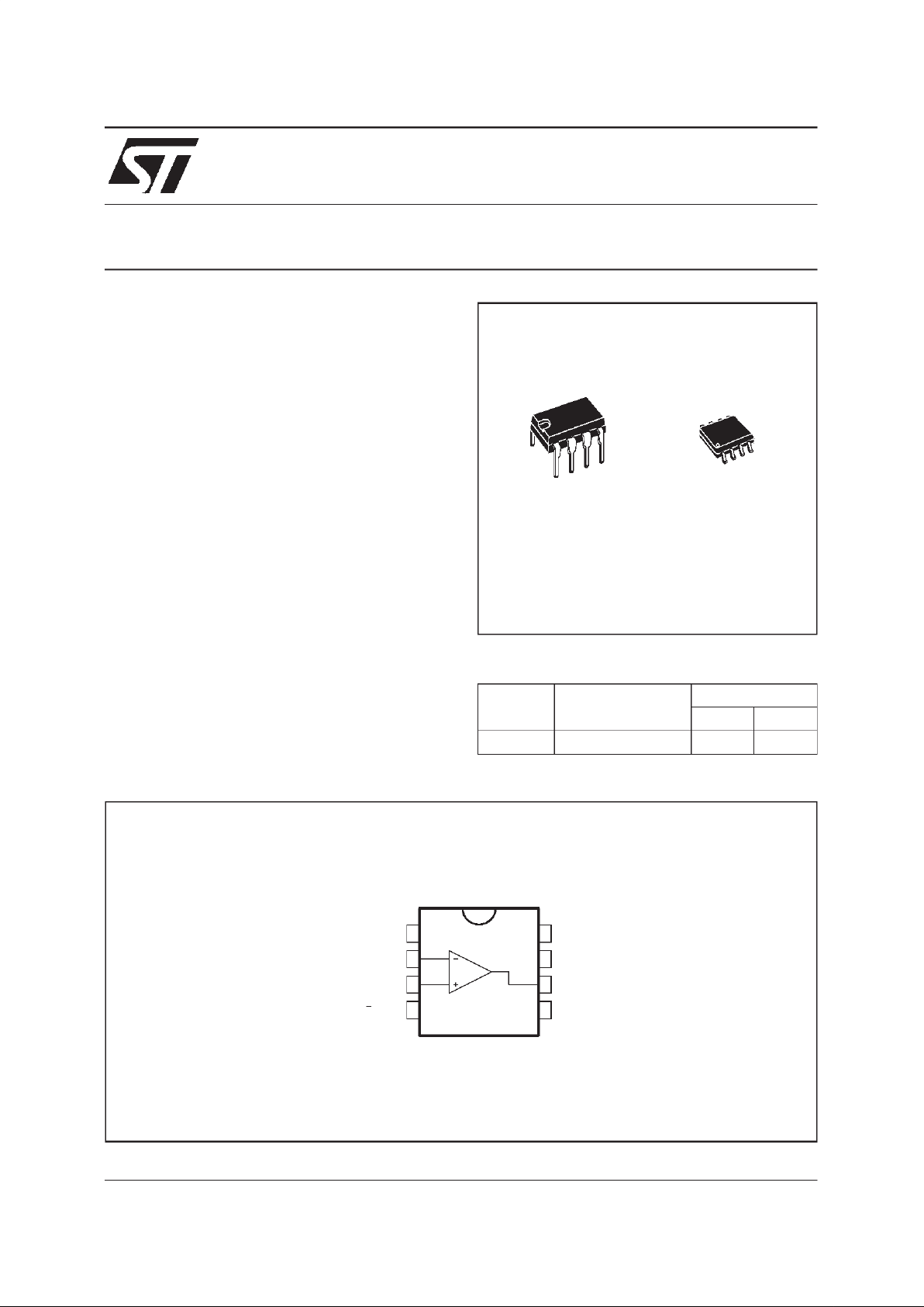
D
SO8
(Plastic Micropackage)
N
DIP8
(Plastic Package)
DESCRIPTION
The TSH11 is a low cost wide bandwidth single
operationalamplifier featuring extremely lowinput
current of 2pA typ. Other features as unity gain
stability,fast settlingtime and highlinearity make it
suitable formanyapplicationsrequiringspeedand
very high input impedance as photo cell amplifier,
high inputimpedancebuffer,Fetprobe, highspeed
precisionintegrator,sample andhold circuit...
1/6
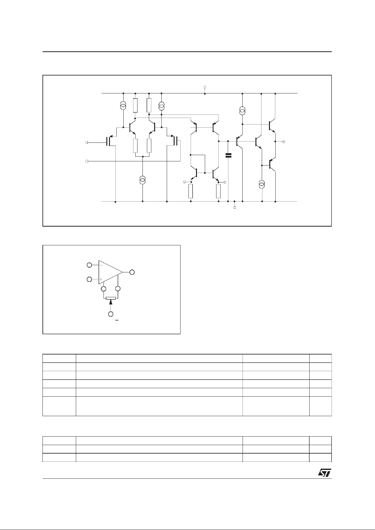
3
non inverting
input
2
inverting
input
1
8
Offset N1
Offse t N2
7V
CC
+
C
c
6
output
Internal
V
CC
-
4
V
ref
SCHEMATICDIAGRAM
ABSOLUTEMAXIMUMRATINGS
Symbol Parameter Value Unit
V
CC
Supply Voltage ±7V
V
id
Differential Input Voltage ±5V
V
i
Input VoltageRange ±5V
I
in
Current On Offset Null Pins ±20 mA
T
oper
Operating Free-Air Temperature Range TSH11C
TSH11I
TSH11M
0
o
C +70
-40
o
C +105
-55
o
C +125
o
C
N1
N2
TSH11
100kΩ
V
CC
INPUT OFFSET VOLTAGENULL CIRCUIT
OPERATINGCONDITIONS
Symbol Parameter Value Unit
V
CC
Supply Voltage ±3to±6V
V
ic
Common Mode Input VoltageRange V
CC
-
to V
CC
+
-3 V
TSH11
2/6

ELECTRICALCHARACTERISTICS
V
CC
= ± 5V, T
amb
=25oC (unless otherwise specified)
Symbol Parameter Min. Typ. Max. Unit
V
io
Input Offset Voltage 3 15 mV
DV
io
Input Offset Voltage Drift
T
min
≤ T
amb
≤ T
max
20
µV/
o
C
I
ib
Input Bias Current 2 300 pA
I
io
Input Offset Current 2 200 pA
I
CC
Supply Current, no load VCC= ± 5V 20 40 mA
A
vd
Large Signal Voltage Gain
V
o
= ±2.5V RL= 100Ω 200 800
V/V
V
icm
Input Common Mode VoltageRange -5 to +2 -5.5 to +2.5 V
CMR Common Mode Rejection Ratio V
ic=Vicm min.
55 95 dB
SVR Supply VoltageRejection Ratio
V
CC
= ± 5V to ± 3V 45 65
dB
V
o
Output Voltage RL= 100Ω ± 2.5 +3.5
-3.7
V
I
o
Output Short Circuit Current
V
id
= ±1V,Vo=0V ±70
mA
GBP Gain Bandwidth Product
A
VCL
= 100, RL= 100Ω, f = 7.5MHz 120
MHz
SR Slew Rate
V
in
= ± 2V,A
VCL
=1,RL= 100Ω 150
V/µs
e
n
Equivalent Input Voltage Noise f = 1MHz 20
nV
√Hz
∅m Phase Margin
A
VM
=1,RL= 100Ω,CL= 15pF 40
Degrees
TSH11
3/6

Input
50
Ω
1k
Ω
10nF
10µF
C
F
-5V
+5V
10nF
Output
50
Ω
10µF
1k
Ω
EVALUATION CIRCUIT
As for any high frequencydevice, a fewrules must
be observedwhendesigningthe PCBtoget the best
performancesfrom your this speed op amp.
From the most to the least important points :
• Each power supply lead has to be bypassed
to ground witha 10nF ceramic capacitor very
close to the device and a 10µF tantalum ca-
pacitor.
• To provide low inductance and low resistance
common return, use a ground plane or common point return for power and signal.
• Allleads must be wide and as short as possible especially for op amp inputs. This is in
order to decrease parasitic capacitance and
inductance.
• Use small resistor values to decrease time
constantwith parasiticcapacitance.
• Choosecomponentsizesassmall aspossible
(SMD).
• On output, decrease capacitor load so as to
avoid circuit stability being degraded which
may cause oscillation. One can also add a
serial resistor in order to minimise its influence.
• One canadd in parallelwith feedbackresistor
a few pF ceramic capacitor C
F
adjusted to
optimizethe settling time.
PRINTEDCIRCUIT LAYOUT
TSH11
4/6

PACKAGEMECHANICAL DATA
8 PINS- PLASTICDIP
Dimensions
Millimeters Inches
Min. Typ. Max. Min. Typ. Max.
A 3.32 0.131
a1 0.51 0.020
B 1.15 1.65 0.045 0.065
b 0.356 0.55 0.014 0.022
b1 0.204 0.304 0.008 0.012
D 10.92 0.430
E 7.95 9.75 0.313 0.384
e 2.54 0.100
e3 7.62 0.300
e4 7.62 0.300
F 6.6 0260
i 5.08 0.200
L 3.18 3.81 0.125 0.150
Z 1.52 0.060
TSH11
5/6

PACKAGEMECHANICAL DATA
8 PINS- PLASTICMICROPACKAGE (SO)
Dimensions
Millimeters Inches
Min. Typ. Max. Min. Typ. Max.
A 1.75 0.069
a1 0.1 0.25 0.004 0.010
a2 1.65 0.065
a3 0.65 0.85 0.026 0.033
b 0.35 0.48 0.014 0.019
b1 0.19 0.25 0.007 0.010
C 0.25 0.5 0.010 0.020
c1 45
o
(typ.)
D 4.8 5.0 0.189 0.197
E 5.8 6.2 0.228 0.244
e 1.27 0.050
e3 3.81 0.150
F 3.8 4.0 0.150 0.157
L 0.4 1.27 0.016 0.050
M 0.6 0.024
S8
o
(max.)
Information furnished is believed to be accurate and reliable. However, STMicroelectronics assumes no responsibility for the
consequences of use of such information nor for any infringement of patents or other rights of third parties which may result from
its use. No license is granted by implication or otherwise under any patent or patent rights of STMicroelectronics. Specifications
mentioned in this publication are subject to change without notice. This publication supersedes and replaces all information
previously supplied. STMicroelectronics products are not authorizedfor useas criticalcomponents inlife supportdevices or systems
without express written approval of STMicroelectronics.
The ST logo is a trademark of STMicroelectronics
1998 STMicroelectronics – Printed in Italy – All Rights Reserved
STMicroelectronics GROUP OF COMPANIES
Australia- Brazil - Canada - China - France - Germany - Italy - Japan - Korea -Malaysia - Malta - Mexico - Morocco
The Netherlands - Singapore - Spain - Sweden - Switzerland - Taiwan- Thailand - United Kingdom - U.S.A.
TSH11
6/6
 Loading...