SGS Thomson Microelectronics TSA1203IFT, TSA1203IF, TSA1203 Datasheet

TSA1203
DUAL-CHANNEL, 12-BIT, 40MSPS, 230mW A/D CONVERTER
■ Low power consumption: 230mW@40Msps
■ Single supply voltage: 2.5V
Independent supply for CMOS output stage
with 2.5V/3.3V capability
■ SFDR= -68.3 dBc @ Fin=10MHz
■ 1GHz analog bandwidth Track-and-Hold
■ Common clocking between channels
■ Dual simultaneous Sample and Hold inputs
■ Multiplexed outputs
■ Built-in reference voltage with external bias
capability
DESCRIPTION
The TSA1203 is a new generati on of high speed,
dual-channel Analog to Digital converter pro-
cessed in a mainstream 0.25µm CMOS techno logy yielding high performances and very low power
consumption.
The TSA1203 is specifically designed for applications requiring very low noise floor, high SFDR
and good isolation b etween channels. It is based
on a pipeline structure and digital error correction
to provide high sta tic linearity at Fs=40M sps, and
Fin=10MHz.
For each channel, a voltage reference is integrated to simplify the design and minimize external
components. It is nevertheless possible to use the
circuit with external references.
Each ADC outputs are multiplexed in a common
bus with small number of pins. A tri-state capability is available for the outputs, allowing chip s election. The inputs of t he ADC must be differentially
driven.
The TSA1203 is available in extended (0 to
+85°C) temperature range, in a small 48 pins
TQFP package.
APPLICATIONS
■ Medical imaging and ultrasound
■ 3G basestation
■ I/Q signal processing applications
■ High speed data acquisition system
■ Portable in st ru me nta t ion
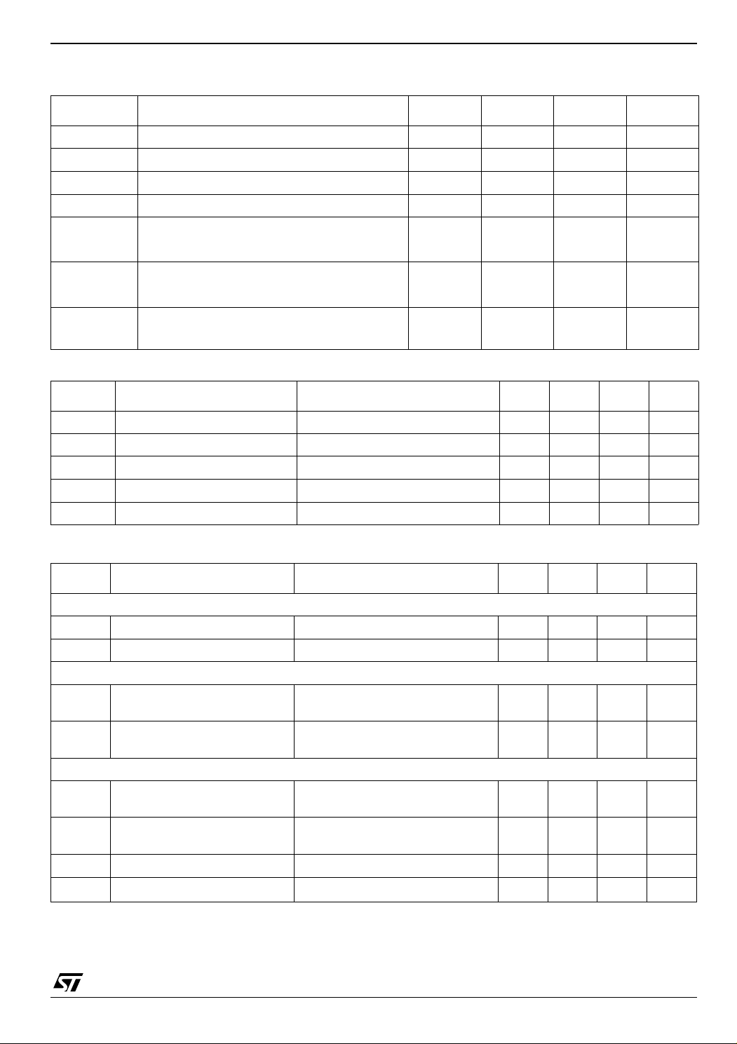
PIN CONNECTIONS (top view)
REFPI
REFMI
INCMI
index
corner
AVCCB
48 44 43 42 41 40 39 38
46 45
47
1
AGND
2
INI
3
AGND
4
INIB
5
AGND
6
IPOL
7
8
AGND
INQ
9
10
AGND
11
INBQ
AGND
12
13 14 15 16 17 18 19 20 21 22
REFPQ
INCMQ
REFMQ
AVCC
AVCC
TSA1203
AGND
AVCC
DVCC
GNDBE
VCCBI
VCCBI
OEB
SELECT
CLK
DGND
BLOCK DIAGRAM
SELECT
CLK
Timing
12
12
GND
M
U
X
VINI
VINBI
VINCMI
VREFMI
IPOL
VINQ
VINBQ
common mode
Polar.
common mode
VREFPI
VREFPQ
VREFMQ
VINCMQ
PACKAGE
+2.5V/3.3V
AD 12
I channel
AD 12
Q channel
REF I
REF Q
DGND
VCCBE
12
D0(LSB)
23 24
DVCC
OEB
D1
37
36
34
33
27
26
25
GNDBI
Buffers
GNDBE
35
32
31
30
29
28
D2
D3
D4
D5
D6
D7
D8
D9
D10
D11(MSB)
VCCBE
GNDBE
VCCBE
12
D0
TO
D11
ORDER CODE
Part Number
TSA1203IF 0°C to +85°C TQFP48 Tray SA120 3I
TSA1203IFT 0°C to +85°C TQFP48 Tape & Reel SA1203I
EVAL1203/BA Evaluation board
February 2003
Temperature
Range
Package Conditioning Marking
7 × 7 mm TQFP48
1/20

TSA1203
CONDITIONS
AVCC = DVCC = VCCB = 2.5V, Fs= 40Msps, Fin=10.13MHz, Vin@ -1dBFS, VREFP=0.8V , VREFM =0V
Tamb = 25°C (unless otherwise specified)
DYNAMIC CHARACTERISTICS
Symbol Parameter Test conditions Min Typ Max Unit
SFDR Spurious Free Dynamic Range -68.3 -59.5 dBc
SNR Signal to Noise Ratio 60.7 66.1 dB
THD Total Harmonics Distortion -66.6 -58 dBc
SINAD Signal to Noise and Distortion Ratio 56.5 62.8 dB
ENOB Effective Number of Bits 9.1 10.3 bits
TIMING CHARACTERISTICS
Symbol Parameter Test conditions Min Typ Max Unit
FS Sampling Frequency 0.5 40 MHz
DC Clock Duty Cycle 45 50 55 %
TC1 Clock pulse width (high) 22.5 25 ns
TC2 Clock pulse width (low) 22.5 25 ns
Tod Data Output Delay (Clock edge to Data Valid) 10pF load capacitance 9 ns
Tpd I Data Pipeline delay for I channel 7 cycles
Tpd Q Data Pipeline delay for Q channel 7.5 cycles
Ton Falling edge of OEB to digital output valid data 1 ns
Toff Rising edge of OEB to digital output tri-state 1 ns
2/20

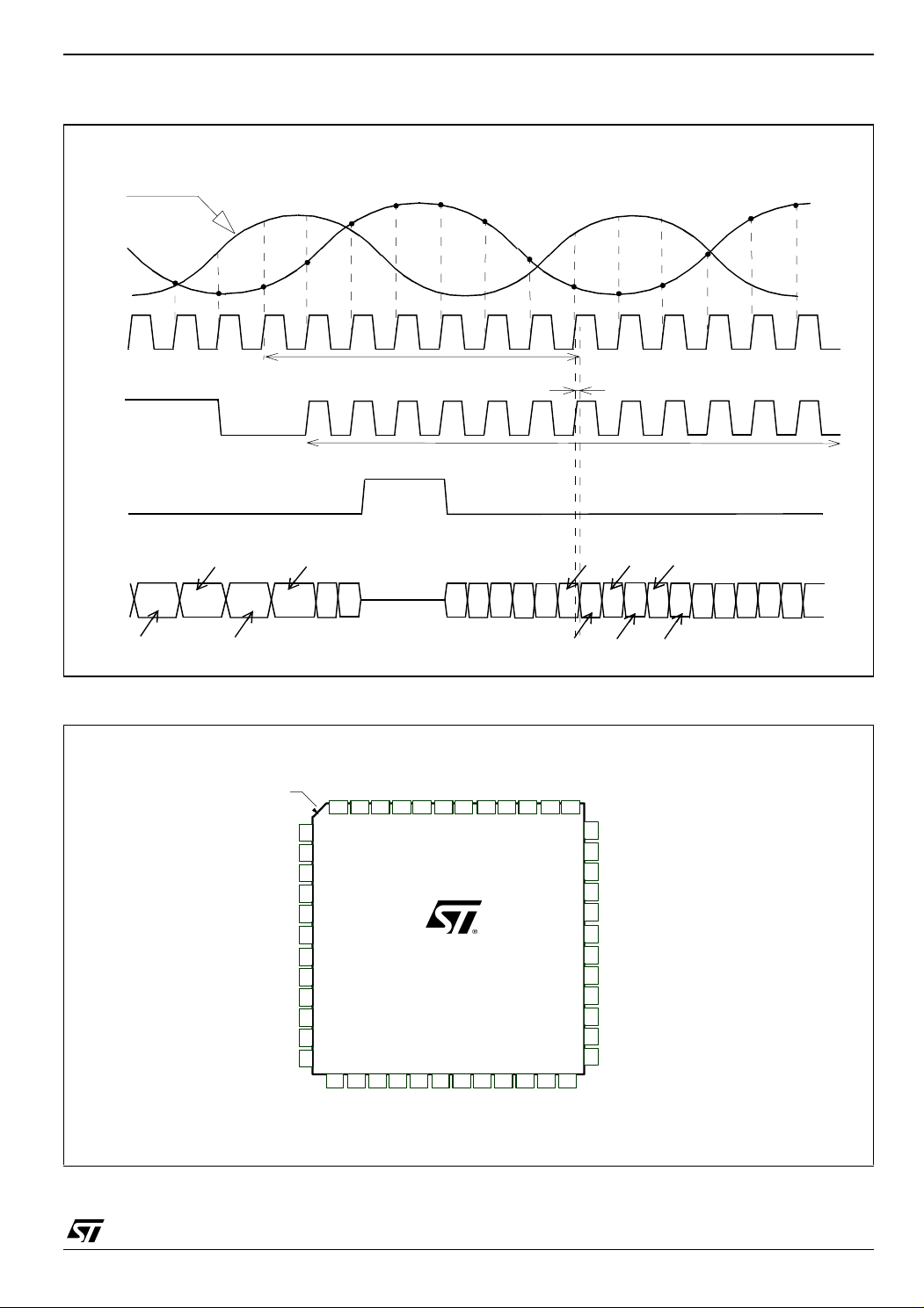
TIMING DIAGRAM
Simultaneous sampling
on I/Q channels
N+3
N+4
N+5
N+6
N+12
TSA1203
N+13
I
Q
CLK
SELECT
OEB
DATA
OUTPUT
sample N-9
I channel
N-1
N
sample N-8
I channel
samp le N-7
Q channel
N+1
N+2
sample N-6
Q channel
PIN CONNECTIONS (top view)
index
corner
1
AGND
2
INI
3
AGND
4
INIB
5
AGND
6
IPOL
7
AVCCB
8
AGND
INQ
9
10
AGND
INBQ
11
AGND
12
N+7
Tpd I + Tod
CLOCK AND SELECT CONNECTED TOGETHER
sample N+1
I channel
GNDBE
REFPI
REFMI
INCMI
AVCC
47
48 44 43 42 41 40 39 38
46 45
VCCBI
AVCC
OEB
VCCBE
VCCBI
TSA1203
13 14 15 16 17 18 19 20 21 22
REFPQ
AGND
AVCC
INCMQ
REFMQ
DVCC
SELECT
CLK
DGND
DGND
sample N
Q channe l
D0(LSB)
37
23 24
DVCC
GNDBI
N+8
D1
N+9
Tod
sample N+1
Q channel
sample N+2
I channel
D2
36
D3
35
D4
34
D5
33
32
D6
31
D7
D8
30
D9
29
D10
28
D11(MSB)
27
26
VCCBE
GNDBE
25
N+10
sample N+2
Q channel
sample N+3
I chan n el
N+11
3/20

TSA1203
PIN DESCRIPTION
Pin No Name Description Observation Pin No Name Description Observatio n
1 AGND Analog ground 0V 25 GNDBE Digital buff er ground 0V
2 INI I channel analog input 26 VCCBE Digital Buffer power supply 2.5V/3.3V
3 AGND Analog ground 0V 27 D11(MSB) Most Significant Bit output CMOS output (2.5V/3.3V)
4 INBI I channel inverted analog input 28 D10 Digital output CMOS output (2.5V/3.3V)
5 AGND Analog ground 0V 29 D9 Digital output C MOS output (2.5V/3.3V)
6 IPOL A nalog bias current input 30 D8 Digit al output CMOS output (2.5V/3.3V)
7 AVCC Analog power supply 2.5V 31 D7 Digital output CMOS output (2.5V/3.3V)
8 AGND Analog ground 0V 32 D6 Digital output C MOS output (2.5V/3.3V)
9 INQ Q channel analog input 33 D5 Digital output CMOS output (2.5V/3.3V)
10 AGND Analog grou nd 0V 3 4 D4 Digital ou tput CMOS output (2. 5V/3.3V)
11 INBQ Q channel inverted analog input 35 D3 Digital output CMOS output (2.5V/3.3V)
12 AGND Analog grou nd 0V 3 6 D2 Digital ou tput CMOS output (2. 5V/3.3V)
13 REFPQ Q channel top reference voltage 37 D1 Digital output CMOS output (2.5V/3.3V)
14 REFMQ Q channel bottom reference
15 INCMQ Q channel input common mode 39 VCCBE Digital Buffer power supply 2.5V/3.3V - See Application
16 AGND Analog grou nd 0V 4 0 GNDBE Digital buffer ground 0V
17 AVCC Analog power supply 2.5V 41 VCCBI Digital Buffer power supply 2.5V
18 DVCC Digital power supply 2.5V 42 VCCBI Digital Buffer powe r s upply 2.5V
19 DGND Digital ground 0V 43 OEB Output Enable input 2.5V/3.3V CMOS input
20 CLK Clock input 2.5V CMOS input 44 AVCC Analog power supply 2.5V
21 SELECT Channel selection 2.5V CMOS input 45 AVCC Analog power supply 2.5V
22 DGND Digital ground 0V 46 INCMI I channel input common mode
23 DVCC Digital power supply 2.5V 47 REFMI I channel bottom reference voltage 0V
24 GNDBI Digital buffer ground 0V 48 REFPI I channel top reference voltage
voltage
0V 38 D0(LSB) Least Significant Bit output CMOS output (2.5V/3.3V)
Note
ELECTRICAL CHARACTERISTICS
ABSOLUTE MAXIMUM RATINGS
Symbol Parameter Values Unit
AVCC
DVCC
VCCBE
VCCBI
Analog Supply voltage
Digital Supply voltage
Digital buffer Supply voltage
Digital buffer Supply voltage
IDout Digital output current -100 to 100 mA
Tstg Storage temperature +150 °C
ESD
HBM: Human Body Model
CDM: Charged Device Model
Latch-up
1). All voltages values, except differential voltage, are with respect to network ground terminal. The magnitude of input and output voltages must not exceed -0.3V or VCC
2). ElectroStatic Discharge pulse (ESD pulse) simulating a human body discharge of 100 pF through 1.5kΩ
3). Discharge to Ground of a device that has been previously charged.
4). Corporate ST Microelectronics procedure number 0018695
Class
4)
1)
1)
1)
1)
2)
3)
0 to 3.3 V
0 to 3.3 V
0 to 3.6 V
0 to 3.3 V
2
1.5
kV
A
4/20

OPERATING CONDITIONS
Symbol Parameter Min Typ Max Unit
AVCC Analog Supply voltage 2.25 2.5 2.7 V
DVCC Digital Supply voltage 2.25 2.5 2.7 V
VCCBE External Digital buffer Supply voltage 2.25 2.5 3.5 V
VCCBI Internal Digital buffer Supply voltage 2.25 2.5 2.7 V
TSA1203
VREFPI
VREFPQ
VREFMI
VREFMQ
INCMI
INCMQ
Forced top voltage reference 0.94 1.4 V
Forced bottom reference voltage 0 0.4 V
Forced input common mode voltage 0.2 1 V
ANALOG INPUTS
Symbol Parameter Test conditions Min Typ Max Unit
VIN-VINB Full scale refere nce voltag e Differential inputs mandatory 1.1 2.0 2 .8 Vpp
Cin Input capacitance 7.0 pF
Req Equivalent input resistor 10 K
BW Analog Input Bandwidth Vin@Full Scale, Fs=40Msps 1000 MHz
ERB Effective Resolution Bandwidth 70 MHz
DIGITAL INPUTS AND OUTPUTS
Symbol Parameter Test conditions Min Typ Max Unit
Clock and Select inputs
VIL Logic "0" voltage 0 0.8 V
VIH Logic "1" voltage 2.0 2.5 V
OEB input
VIL Logic "0" voltage 0
VIH Logic "1" voltage
Digital Outputs
VOL
VOH
IOZ High Impedance leakage current OEB set to VIH -1.67 0 1.67 µA
Logic "0" voltage
Logic "1" voltage
C
Output Load Capacitance 15 pF
L
Iol=10µA
Ioh=10µA 0.9 x
0.75 x
VCCBE
VCCBE
VCCBE V
VCCBE V
0.25 x
VCCBE
0.1 x
0
VCCBE
Ω
V
V
5/20

TSA1203
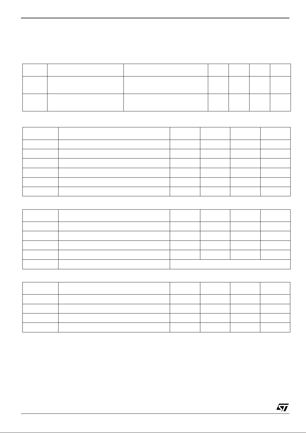
CONDITIONS
AVCC = DVCC = VCCB = 2.5V, Fs= 40Msps, Fin=2MHz, Vin@ -1dBFS, VREFP=0.8V, VREFM=0V
Tamb = 25°C (unless otherwise specified)
REFERENCE VOLTAGE
Symbol Parameter Test conditions Min Typ Max Unit
VREFPI
VREFPQ
VINCMI
VINCMQ
POWER CONSUMPTION
Top internal reference voltage 0.81 0.88 0.94 V
Input common mode voltage 0.41 0.46 0.50 V
Symbol Parameter Min Typ Max Unit
ICCA Analog Supply current 82 96.5 mA
ICCD Digital Supply Current 4.4 4.9 mA
ICCBE Digital Buffer Supply Current (10pF load) 6.6 9.4 mA
ICCBI Digital Buffer Supply Current 274 440
Pd Power consumption in normal operation mode 230 271 mW
Rthja Thermal resistance (TQFP 48) 80 °C/W
ACCURACY
Symbol Parameter Min Typ M ax Unit
OE Offset Error 2.97 LSB
GE Gain Error 0.1 %
DNL Differential Non Linearity ±0.52 LSB
INL Integral Non Linearity ±3 LSB
- Monotonicity and no missing codes Guaranteed
A
µ
MATCHING BETWEEN CHANNELS
Symbol Parameter Min Typ Max Unit
GM Gain match 0.04 1 %
OM Offset match 0.88 LSB
PHM Phase match 1 dg
XTLK Crosstalk rejection 85 dB
6/20
 Loading...