

SGS Thomson Microelectronics TSA1005-40IF, TSA1005-20IFT, TSA1005-20IF, TSA1005, TSA1005-40IFT Datasheet
1/22
■ 10-bit, dual-channel A/D converter in deep
submicron CMOS technology, 20/40Msps
■ Single supply voltage: 2.5V
Independent supply for CMOS output stage
with 2.5V/3.3V capability
■ ENOB=9.5 @ 20Msps, ENOB=9.2 @
40Msps, Fin=10MHz
■ SFDR typically up to 62.5dB @ 40Msps,
Fin=10MHz.
■ 1GHz analog bandwidth Track-and-Hold
■ Common clocking between channel s
■ Multiplexed outputs
DESCRIPTION
The TSA1005 belongs to a new generation of high
speed, dual-channel Anal og to Digital conv erters,
processed in a mainstream 0.25 µm CMOS technology and yielding high performances.
The TSA1005 is specifically designed for applications requiring a very low noise floor, high SFDR
and good isolation b etween channels. It is bas ed
on a pipeline structure and digital error correction,
providing high static linearity at 20/40 Msp, and
Fin = 10 MHz.
For each channel, a voltage reference is integrated to simplify the design and minimize external
components. It is nevertheless possible to use the
circuit with external references.
Each ADC output is multiplexed on a common bus
with small number of pins. A tri-state capability is
available for the output signals, a llowing for chip
selection. The input signals of the ADC mus t be
differentially driven.
The TSA1005 is supports an extended (0 to
+85°C) temperature range , and is available in the
small 48-pin TQFP package.
APPLICATIONS
■ Medical imaging and ultrasound
■ I/Q signal processing applications
■ High speed data acquisition system
■ Portable instrumentation
■ High resolution fax and scanners
ORDER CODE
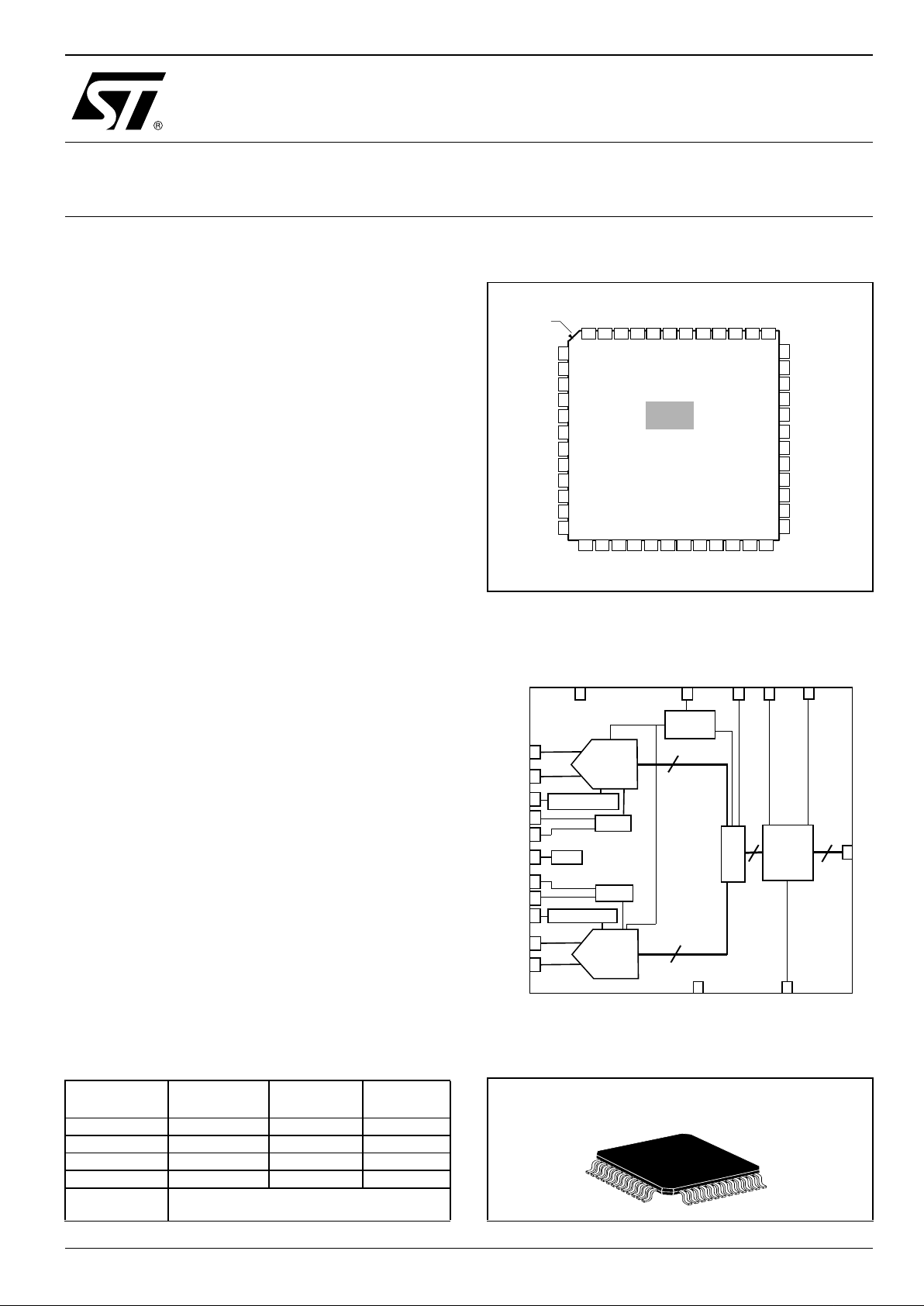
PIN CONNECTIONS (top view)
BLOCK DIAGRAM
PACKAGE
Part Number
Temperature
Range
Status Conditioning
TSA100 5-20IF -40°C to +85°C Sample Tr ay
TSA1005-20IFT -40°C to +85°C Sample Tape & Reel
TSA1005I-40IF 0°C to +85°C Production Tray
TSA1005-40IFT 0°C to +85°C Production T ape & Reel
EVAL1005-20/BA
EVAL1005-40/BA
Evaluation board
D3
D4
D5
D6
D7
D8
D9(MSB)
AVCCB
index
corner
1
2
3
4
5
6
7
8
9
10
11
32
31
30
29
28
27
26
13 14 15 16 17 18 19 20 21 22
47
25
33
12
23 24
35
34
36
48 44 43 42 41 40 39 38
37
46 45
TSA1005
VCCBE
GNDBE
AGND
INI
AGND
AGND
IPOL
AGND
AGND
INBQ
INIB
AGND
INQ
D0(LSB)
D1
REFMI
NC
OEB
AVCC
REFPI
INCMI
AVCC
VCCBI
GNDBE
VCCBI
NC
VCCBE
SELECT
CLK
DGND
REFPQ
AGND
AVCC
DGND
DVCC
DVCC
INCMQ
REFMQ
GNDBI
D2
Timing
Buffers
IPOL
CLK
+2.5V/3.3V
VINI
VINBI
OEB
VINCMI
GND
VINQ
VINBQ
VINCMQ
AD 10
I channel
AD 10
Q channel
10
10
10
10
M
U
X
REF I
REF Q
SELECT
VREFPI
VREF PQ
Polar.
VREFMI
VREFM Q
common mod e
common mode
D0
TO
D9
GNDBE
VCCBE
7 × 7 mm TQFP48
TSA1005
DUAL-CHANNEL, 10-BIT, 20/40MSPS A/D CONVERTER
June 2003
TSA1005
2/22
ABSOLUTE MAXIMUM RATINGS
OPERATING CONDITIONS
Symbol Parameter Values Unit
AVCC
Analog Supply voltage
(1)
0 to 3.3 V
DVCC
Digital Supply voltage
1)
0 to 3.3 V
VCCBE
Digital buffer Supply voltage
1)
0 to 3.6 V
VCCBI
Digital buffer Supply voltage
1)
0 to 3.3 V
IDout Digital output current -100 to 100 mA
Tstg Storage temperature +150 °C
ESD
HBM: Human Body Model
(2)
CDM: Charged Device Model
(3)
2
1.5
kV
Latch-up
Class
(4)
A
1 All voltage values, except for differential voltage, are with respect to the network ground terminal. The magnitude of input and output volt-
ages must not excee d -0.3 V or VCC
2 ElectroStatic Discharge pulse (ESD pulse) simulating a human body discharge of 100 pF through 1.5 k
Ω
3 Discha rge to Ground of a device that has been prev i ously charged.
4 Corpor ate ST Microel ectronics procedure nu mber 001869 5
Symbol Parameter
TSA1005-20
(1)
TSA1005-40
Min. Typ. Max. Min. Typ. Max. Unit
AVCC Analog Supply voltage 2.25 2.5 2.7 2.25 2.5 2.7 V
DVCC Digital Supply voltage 2.25 2.5 2.7 2.25 2.5 2.7 V
VCCBE External Digital buffer Supply voltage 2.25 2.5 3.5 2.25 2.5 3.5 V
VCCBI Internal Digital buffer Supply voltage 2.25 2.5 2.7 2.25 2.5 2.7 V
VREFPI
VREFPQ
Forced top voltage reference 0.94 1.4 0.94 1.4 V
VREFMI
VREFMQ
Forced bottom reference voltage 0 0.4 0 0.4 V
INCMI
INCMQ
Forced input common mode voltage 0.2 1 0.2 1 V
TSA1005
3/22
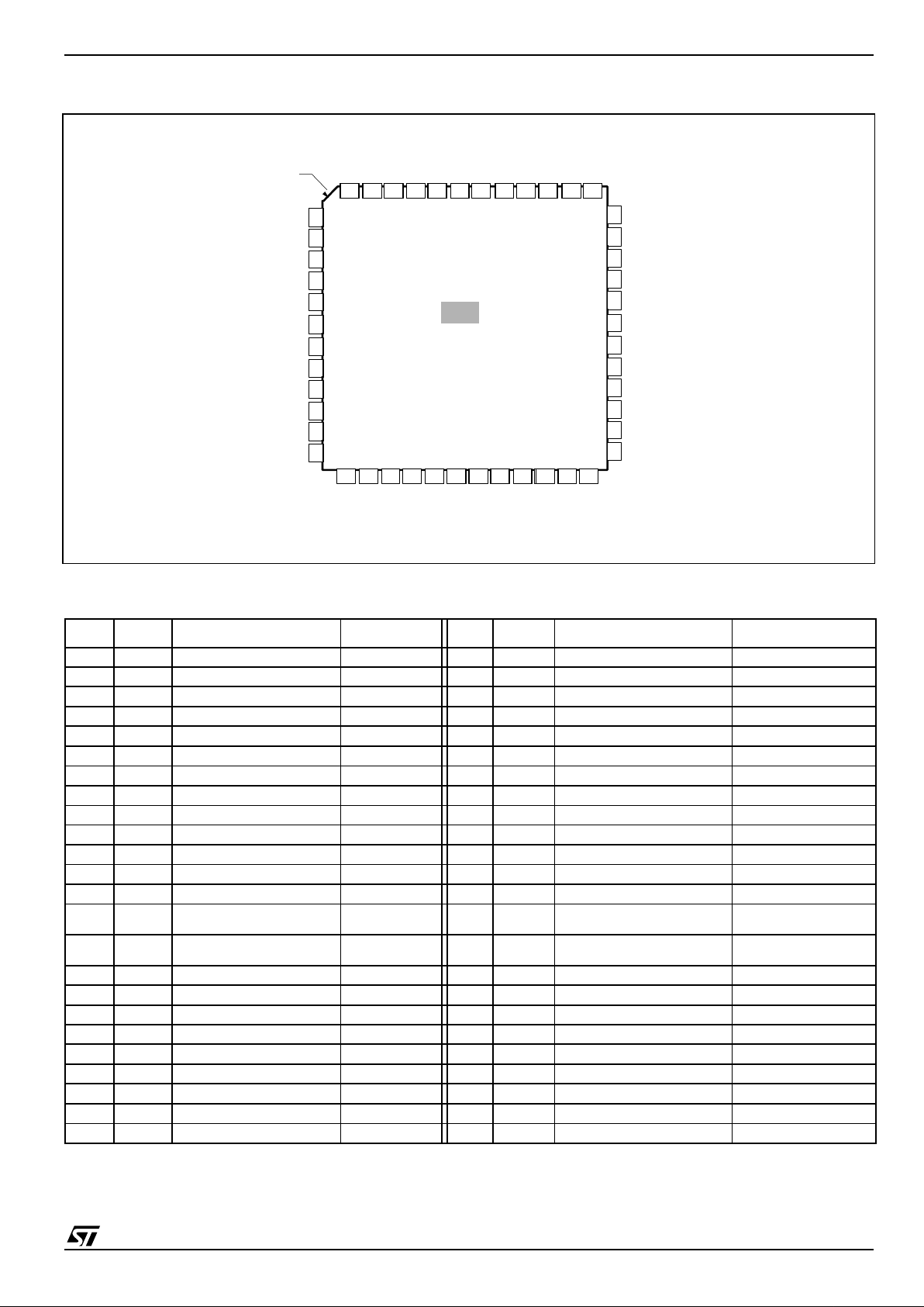
PIN CONNECTIONS (top view)
PIN DESCRIPTION
D3
D4
D5
D6
D7
D8
D9(MSB)
AVCCB
index
corner
1
2
3
4
5
6
7
8
9
10
11
32
31
30
29
28
27
26
13 14 15 16 17 18 19 20 21 22
47
25
33
12
23 24
35
34
36
48 44 43 42 41 40 39 38
37
46 45
TSA1005
VCCBE
GNDBE
AGND
INI
AGND
AGND
IPOL
AGND
AGND
INBQ
INIB
AGND
INQ
D0(LSB)
D1
REFMI
NC
OEB
AVCC
REFPI
INCMI
AVCC
VCCBI
GNDBE
VCCBI
NC
VCCBE
SELECT
CLK
DGND
REFPQ
AGND
AVCC
DGND
DVCC
DVCC
INCMQ
REFMQ
GNDBI
D2
Pin No Name Description Observation Pin No Name Description Observation
1 AGND Analog gro und 0V 25 GNDBE Digital buffer ground 0V
2 INI I channel analog input 26 VCCBE Digital Buffer power supply 2.5V/3.3V
3 AGND Analog ground 0V 27 D9(MSB) Most Significant Bit output CMOS output (2.5V/3.3V)
4 INBI I channel inverted analog input 28 D8 Digital output CMOS output (2.5V/3.3V)
5 AGND Analog ground 0V 29 D7 Digital output CMOS output (2.5V/3.3V)
6 IPOL Ana l og bias current input 30 D6 Digital output CMOS output (2.5V/3 .3V)
7 AVCC Analog power s upply 2.5V 31 D5 Digital output CMOS outp ut (2.5 V/3.3V)
8 AGND Analog ground 0V 32 D4 Digital output CMOS output (2.5V/3.3V)
9 INQ Q channel analog input 33 D3 Digital output CMOS output (2.5V/3.3V)
10 AGND Analog ground 0V 34 D2 Digital output CMOS output (2.5V/3.3V)
11 INBQ Q channel inverted analog input 35 D1 Digital output CMOS output (2.5V/3.3V)
12 AGND Analog ground 0V 36 D0(LSB) Least Significant Bit output CMOS output (2.5V/3.3V)
13 REFPQ Q channel top reference voltage 37 NC Non connected
14 REFMQ Q channel bottom reference
voltage
0V 38 NC Non connected
15 INCMQ Q channel input common mode 39 VCCBE Digital Buffer power supply 2.5V/3.3V - See Application
Note
16 AGND Analog ground 0V 40 GNDBE Digital buffer ground 0V
17 AVCC Analog power supply 2.5V 41 VCCBI Digital Buffer power supply 2.5V
18 DVCC Digital power supply 2.5V 42 VCCBI Digital Power Supply 2.5V
19 DGND Digita l ground 0V 43 OEB Output Enable input 2.5V/3.3V CMOS input
20 CLK Clock input 2.5V CMOS input 44 AVCC Analog power supply 2.5V
21 SELECT Channel selection 2.5V CMOS input 45 AVCC Analog power supply 2.5V
22 DGND Digita l ground 0V 46 INCM I I channel input common mode
23 DVCC Digital power sup ply 2.5V 47 REFMI I channel bottom ref erenc e voltage 0V
24 GNDBI Digital buffer ground 0V 48 REFPI I chan nel top refer ence voltage
TSA1005
4/22
ELECTRICAL CHARACTERISTICS
AVCC = DVCC = VCCB = 2.5 V, Fs = 20/40 Msps, Fin = 10.13 MHz, Vin@ -1 dBFS, VREFP = 0.8 V,
VREFM = 0 V
Tamb = 25°C (unless otherwise specified)
TIMING CHARACTERISTICS
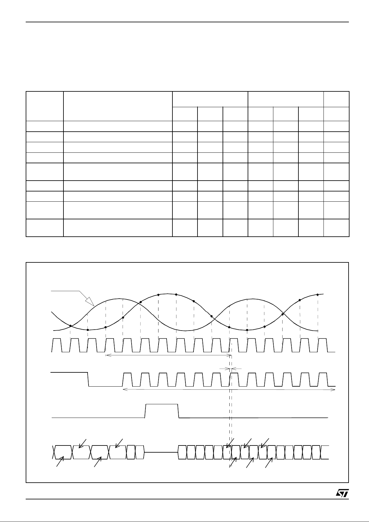
TIMING DIAGRAM
Symbol Parameter.
TSA1005-20
(1)
1 P reliminary data.
TSA1005-40
Min. Typ. Max. Min. Typ. Max. Unit
FS Sampling Frequency 0.5 20 0.5 40 MHz
DC Clock Duty Cycle 50 45 50 55 %
TC1 Clock pulse width (high) 25 12.5 ns
TC2 Clock pulse width (low) 25 12.5 ns
Tod
Data Output Delay (Clock edge to Data
Valid) - 10pF load capacitance
55ns
Tpd I Data Pipeline delay for I channel 7 7 cycles
Tpd Q Data Pipeline delay for Q channel 7.5 7.5 cycles
Ton
Falling edge of OEB to digital output
valid data
11ns
Toff
Rising edge of OEB to digital output
tri-state
11ns
N-1
N
N+1
N+6
N+7
N+2
N+5
N+3
N+4
N+8
CLK
Tpd I + Tod
N+9
N+10
N+11
N+12
N+13
DATA
OUTPUT
sample N+1
I channel
sample N
Q channel
sample N+1
Q channel
sample N+2
I channel
sample N+2
Q channel
sample N+3
I channel
OEB
Simultaneous sampling
on I/Q channels
SELECT
sample N-9
I channel
sample N-8
I channel
samp le N-7
Q channel
sample N-6
Q channel
CLOCK AND SELECT CONNECTED TOGETHER
Tod
I
Q
TSA1005
5/22
CONDITIONS
A VCC = DVCC = VCCB = 2.5V , Fs= 20/40Msps, Fin=2MHz, Vin@ -1dBFS, VREFM=0V
Tamb = 25°C (unless otherwise specified)
ANALOG INPUTS
DIGITAL INPUTS AND OUTPUTS
REFERENCE VOLTAGE
Symbol Parameter
TSA1005-20
(1)
TSA1005-40
Min. Typ. Max. Min. Typ. Max. Unit
VIN-VINB Full scale reference voltage 1.1 2.0 2.8 1.1 2.0 2.8 Vpp
Cin Input capacitance 7.0 7 pF
Req Equivalent input resistor 3.3 1.6 K
Ω
BW
Analog Input Bandwidth
Vin Full scale, Fs max
1000 1000 MHz
ERB Effective Resolution Bandwidth 70 70 MHz
1 P reliminary data
Symbol Parameter Test conditions Min Typ Max Unit
Clock and Select inputs
VIL Logic "0" voltage 0 0.8 V
VIH Logic "1" voltage 2.0 2.5 V
OEB input
VIL Logic "0" voltage 0
0.25 x
VCCBE
V
VIH Logic "1" voltage
0.75 x
VCCBE
VCCBE V
Digital Outputs
VOL
Logic "0" voltage
Iol=10µA
0
0.1 x
VCCBE
V
VOH
Logic "1" voltage
Ioh=10µA 0.9 x
VCCBE
VCCBE V
IOZ High Impedance leakage current OEB set to VIH -1.67 0 1.67 µA
C
L
Output Load Capacitance 15 pF
Symbol Parameter
TSA1005-20
(1)
TSA1005-40
Min. Typ. Max. Min. Typ. Max. Unit
VREFPI
VREFPQ
Top internal reference voltage 0.81 0.88 0.94 0.81 0.88 0.94 V
VINCMI
VINCMQ
Input common mode voltage 0.41 0.46 0.50 0.41 0.46 0.50 V
TSA1005
6/22
CONDITIONS
AVCC = DVCC = VCCB = 2.5V, Fs= 20/40Msps, Fin=2MHz, Vin@ -1dBFS, VREFP=0.8V, VREFM=0V
Tamb = 25°C (unless otherwise specified)
POWER CONSUMPTION
ACCURACY
DYNAMIC CHARACTERISTICS
MATCHING BETWEEN CHANNELS
Symbol Parameter
TSA1005-20
(1)
TSA1005-40
Min. Typ. Max. Min. Typ. Max. Unit
ICCA Analog Supply current 30 69.5 72.8 mA
ICCD Digital Supp ly Current 4 3.5 3.6 mA
ICCBE
Digital Buffer Supply Current (10pF
load)
6 6.5 6.9 mA
ICCBI Digital Buffer Supply Current 274 131 149 u A
Pd
Power consumption in normal operation mode
100 199.5 207.7 mW
Rthja Thermal resistance (TQFP48) 80 80 °C/W
Symbol Parameter
TSA1005-20
(1)
TSA1005-40
Min. Typ. Max. Min. Typ. Max. Unit
OE Offset Error 2.97 2.97 LSB
GE Gain Error 0.1 0.1 %
DNL Differential Non Linearity ±0.5 ±0.6 LSB
INL Integral Non Linearity ±0.7 ±1 LSB
- Monotonicity and no missing codes Guaranteed Guaranteed
Symbol Symbol
TSA1005-20
(1)
TSA1005-40
Min. Typ. Max. Min. Typ. Max. Unit
SFDR
Spurious Free Dynamic Range -73 -62.6 -58.1 dBc
SNR
Signal to Noise Ratio 60 57.1 59.8 dB
THD
Total Harmonics Distortion -73 -62 -57.5 dBc
SINAD
Signal to Noise and Distortion Ratio 59 54.9 57.3 dB
ENOB
Effective number of bits 9.5 8.8 9.2 bits
Symbol Parameter
TSA1005-20
(1)
TSA1005-40
Min. Typ. Max. Min. Typ. Max. Unit
GM Gain match 0.04 0.04 1 %
OM Offset match 0.5 0.5 LSB
PHM P hase match 1 1 dg
XTLK Crosstalk rejection 85 85 dB
1 Pre lim i nary data
TSA1005
7/22
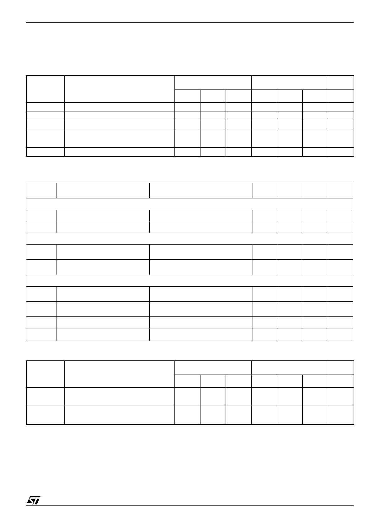
Static parameter: Integral Non Linearity
Fs=20MSPS; Icca= 30mA ; Fin=10M Hz
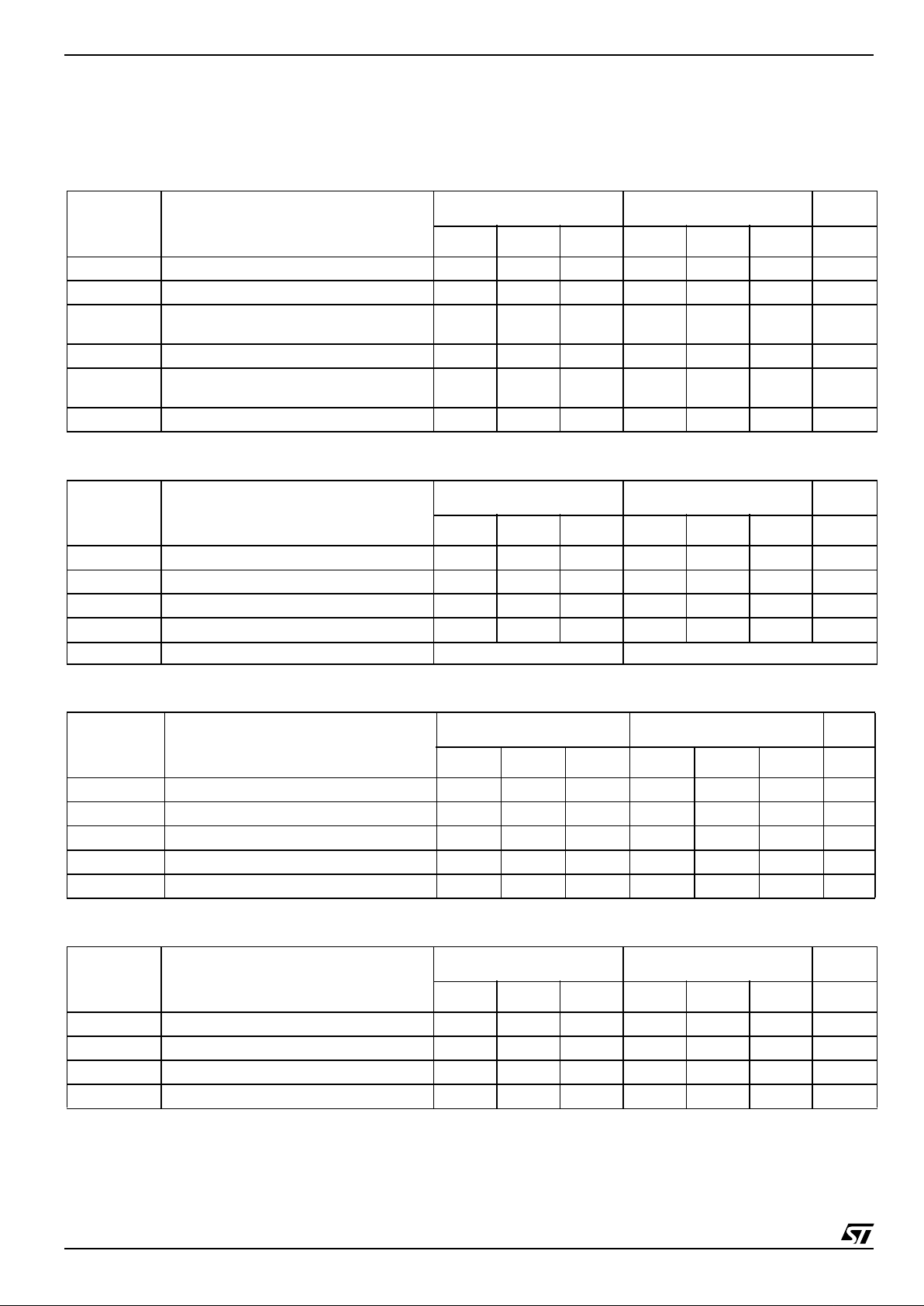
Static parameter: Integral Non Linearity
Fs=40MSPS; Icca= 45mA ; Fin=10M Hz
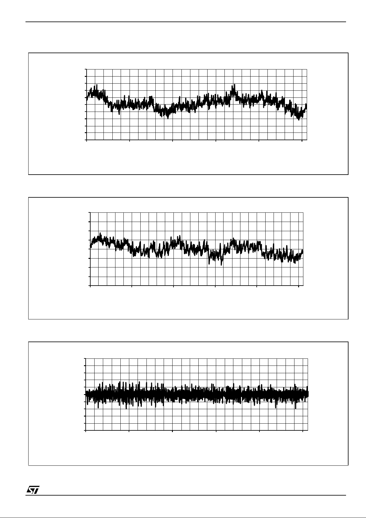
Static parameter: Differential Non Linearity
Fs=20MSPS; Icca= 30mA ; Fin=10M Hz
-1
-0.8
-0.6
-0.4
-0.2
0
0.2
0.4
0.6
0.8
1
0 200 400 600 800 1000
Ou t put Co de
INL (LSBs)
-2
-1.5
-1
-0.5
0
0.5
1
1.5
2
0 200 400 600 800 1000
Ou t put Co de
INL (LSBs)
-1
-0.8
-0.6
-0.4
-0.2
0
0.2
0.4
0.6
0.8
1
0 200 400 600 800 1000
Output Code
DNL (LSBs)
 Loading...