

SGS Thomson Microelectronics TSA0801IF Datasheet
TSA0801
8-BIT, 40MSPS, 40mW A/D CONVERTER
■ 8-bit A/D converter in deep submicron
CMOS technology
■ Single supply voltage: 2.5V
■ Input range: 2Vpp differential
■ 40Msps sampling frequency
■ Ultra low power consumption: 40mW @
40MHz (10mW @ 5Msps)
■ ENOB=7.9 @ Nyquist
■ SFDR typically up to 67dB @ Fs=40Msps,
Fin=5MHz
■ Built-in reference voltage with external bias
capability
■ STMicroelectronics 8,10, 12 and 14-bits ADC
pinout compatibility
DESCRIPTION
The TSA0801 is an 8-bit, 40MHz sampling frequency Analog to Digital converter using a deep
submicron CMOS technology combining high performances and very low power consumption.
The TSA0801 is based on apipeline structure and
digital error correction to provide excellent static
linearity and go beyond 7.9 effective bits at
Fs=40Msps, and Fin=10MHz.
A voltage reference is integrated in the circuit to
simplify the design and minimize external components. It is nevertheless possible to usethe circuit
with an external reference.
Differential or single-ended analog inputs can be
applied to the converter. A tri-state capability is
available on the outputs. The output data can be
coded into two different formats. A Data Ready
signal is raised as the data is valid on the output
and can be used for synchronization purposes.
The TSA0801 is available in commercial (0 to
+70°C) and extended (-40 to +85°C) temperature
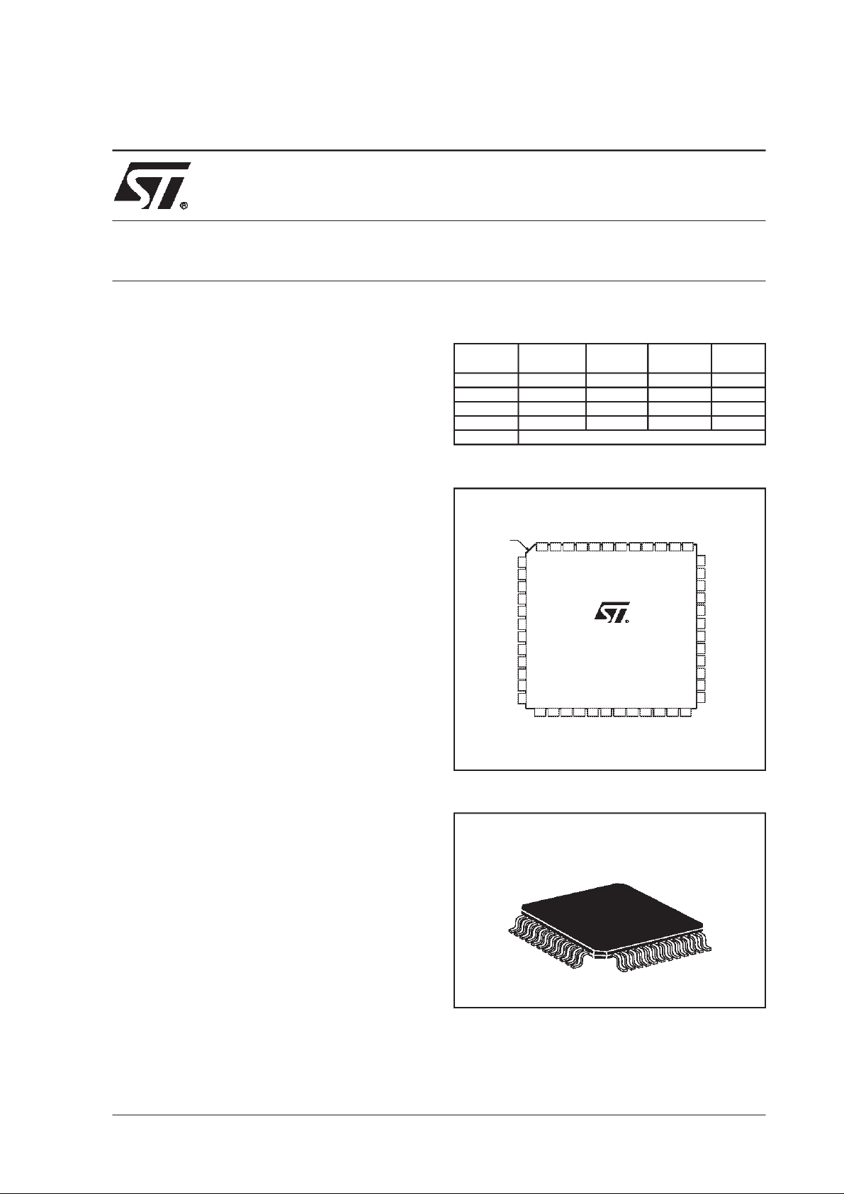
range, in a small 48 pins TQFPpackage.
ORDER CODE
Part Number
TSA0801CF 0°C to +70°C TQFP48 Tray SA0801C
TSA0801CFT 0°Cto +70°C TQFP48 Tape& Reel SA0801C
TSA0801IF -40°Cto +85°C TQFP48 Tray SA0801I
TSA0801IFT -40°C to +85°C TQFP48 Tape& Reel SA0801I
EVAL0801/AA Evaluation board
Temperature
Range
Package Conditioning Marking
PIN CONNECTIONS (top view)
AGND
index
corner
IPOL
VREFP
VREFM
AGND
VIN
AGND
VINB
AGND
INCM
AGND
AVCC
AVCC
AVCC
DFSB
48 44 43 42 41 40 39 38
46 45
47
1
2
3
4
5
6
7
8
9
10
11
12
13 14 15 16 17 18 19 2 0 21 22
DVCC
DVCC
DGND
TSA0801
CLK
OEB
DGND
VCCB
GNDB
NC
DGND
GNDB
GNDB
VCCB
23 24
VCCBNCOR
NC
DR
37
NC
36
NC
35
NC
34
33
NC
32
NC
31
D0(LSB)
30
D1
D2
29
D3
28
D4
27
26
D5
25
D6AVCC
D7 (MSB)
NC
PACKAGE
7 × 7 mm TQFP48
APPLICATIONS
■ Hand-held instrumentation
■ Camcorders
■ Computer scanners
■ Digital communication
October 2000
1/20
TSA0801
ABSOLUTE MAXIMUM RATINGS
Symbol Parameter Values Unit
AVCC
DVCC
VCCB
Analog Supply voltage
Digital Supply voltage
Digital buffer Supply voltage
1)
1)
1)
IDout Digital output current -100 to 100 mA
Tstg Storage temperature +150 °C
Electrical Static Discharge:
ESD
- HBM
- CDM-JEDEC Standard
1) All voltages values, except differential voltage, are with respect to network ground terminal. The magnitude of input and output voltages
must never exceed -0.3V or VCC+0V
OPERATING CONDITIONS
Symbol Parameter Test conditions Min Typ Max Unit
AVCC Analog Supply voltage 2.25 2.5 2.7 V
DVCC Digital Supply voltage 2.25 2.5 2.7 V
VCCB Digital buffer Supply voltage 2.25 2.5 2.7 V
VREFP Forced top voltage reference 1.16 - AVCC V
VREFM Forced bottom reference voltage 0 0 0.5 V
0 to 3.3 V
0 to 3.3 V
0 to 3.3 V
2
KV
1.5
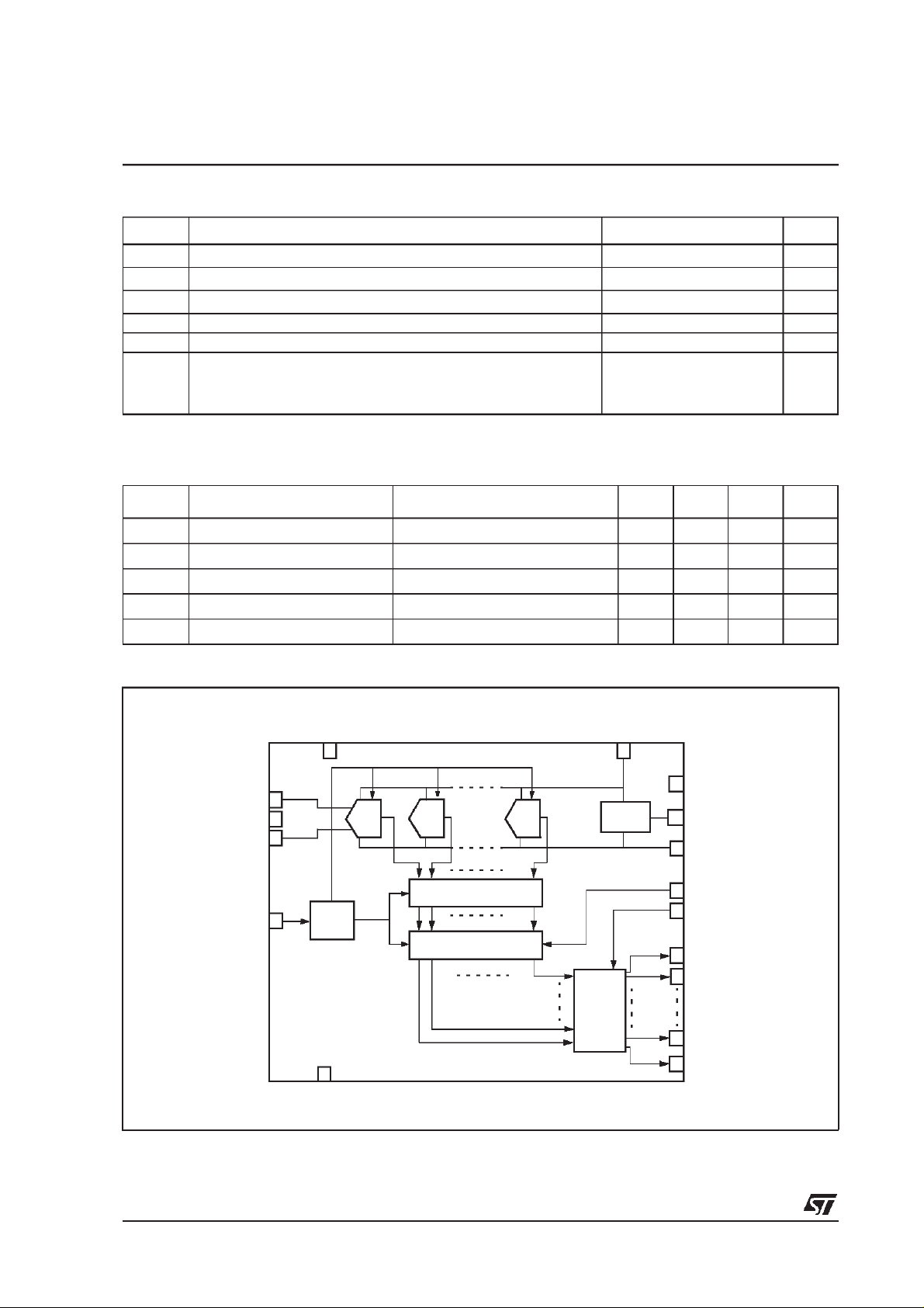
BLOCK DIAGRAM
INCM
VINB
CLK
VIN
+2.5V
stage stage stage
12 n
Sequencer-phase shifting
Timing
Digitaldata correction
GND
Buffers
VREFP
Reference
circuit
GNDA
IPOL
VREFM
DFSB
OEB
DR
DO
TO
D7
OR
2/20
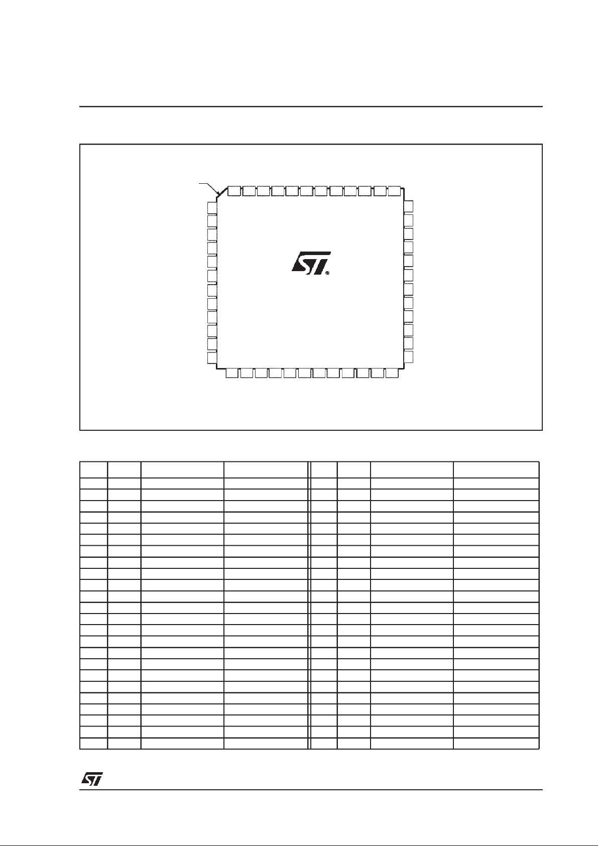
PIN CONNECTIONS (top view)
TSA0801
PIN DESCRIPTION
index
corner
IPOL
VREFP
VREFM
AGND
VIN
AGND
VINB
AGND
INCM
AGND
AVCC
AGND
AVCC
AVCC
DFSB
OEB
NC
NC
47
48 44 43 42 41 40 39 38
46 45
1
2
3
4
5
6
7
8
9
10
11
12
13 14 15 16 17 18 19 20 21 22
DVCC
DVCC
TSA0801
CLK
DGND
DGND
DGND
VCCB
GNDB
GNDB
GNDB
VCCB
DR
23 24
VCCBNCOR
NC
37
D7 (MSB)
36
35
34
33
32
31
30
29
28
27
26
25
NC
NC
NC
NC
NC
D0(LSB)
D1
D2
D3
D4
D5
D6AVCC
Pin No Name Description Observation Pin No Name Description Observation
1 IPOL Analog bias currentinput 25 D6 Digital output CMOS output (2.5V)
2 VREFP Top voltage reference 1V 26 D5 Digital output CMOS output (2.5V)
3 VREFM Bottom voltage referen ce 0V 27 D4 Digital output CMOS output (2.5V)
4 AGND Analog ground 0V 28 D3 Digital output CMOS output (2.5V)
5 VIN Analog input 1Vpp 29 D2 Digital output CMOS output (2.5V)
6 AGND Analog ground 0V 30 D1 Digital output CMOS output (2.5V)
7 VINB Inverted analog input 1Vpp 31 D0(LSB) Digital output CMOS output (2.5V)
8 AGND Analog ground 0V 32 NC Non conne cted
9 INCM Input common mode 0.5V 33 NC Non conne cted
10 AGND Analog ground 0V 34 NC Non connected
11 AVCC Analog power supply 2.5V 35 NC Non connected
12 AVCC Analog power supply 2.5V 36 NC Non conne cted
13 DVCC Digital power supply 2.5V 37 NC Non conne cted
14 DVCC Digital power supply 2.5V 38 DR Data Ready output CMOS output (2.5V)
15 DGND Digital ground 0V 39 VCCB Digital Buffer power supply 2.5V
16 CLK Clock input 2.5V compatibleCMOS input 40 GNDB Digital Buffer ground 0V
17 DGND Digital ground 0V 41 VCCB Digital Buffer power supply 2.5V
18 NC Non connected 42 NC Non conne cted
19 DGND Digital ground 0V 43 NC Non conne cted
20 GNDB Digital buffer ground 0V 44 OEB Output Enable input 2.5V compatibleCMOS input
21 GNDB Digital buffer ground 0V 45 DFSB Data Format Select input 2.5Vcompatib le CMOS input
22 VCCB Digital bufferpower supply 2.5V 46 AVCC Analog power supply 2.5V
23 OR Out Of Range output CMOS output(2.5V) 47 AVCC Analog power supply 2.5V
24 D7(MSB) Most SignificantBit output CMOS output(2.5V) 48 AGND Analog ground 0V
3/20
TSA0801
ELECTRICAL CHARACTERISTICS
AVCC= DVCC = VCCB =2.5V,Fs= 40Msps,Fin=1MHz, Vin@ -1.0dBFS, VREFM = 0V
Tamb = 25°C (unless otherwise specified)
TIMING CHARACTERISTICS
Symbol Parameter Test conditions Min Typ Max Unit
FS Sampling Frequency 0.5 40 MHz
DC Clock Duty Cycle 45 50 55 %
TC1 Clock pulse width (high) 11 12.5 ns
TC2 Clock pulse width (low) 11 12.5 ns
Tod
Data Output Delay (Fall of Clock
to Data Valid)
Tpd Data Pipeline delay 6.5 cycles
Ton
Toff
Falling edge of OEB to digital
output valid data
Rising edge of OEB to digital
output tri-state
10pF load capacitance
5ns
1ns
1ns
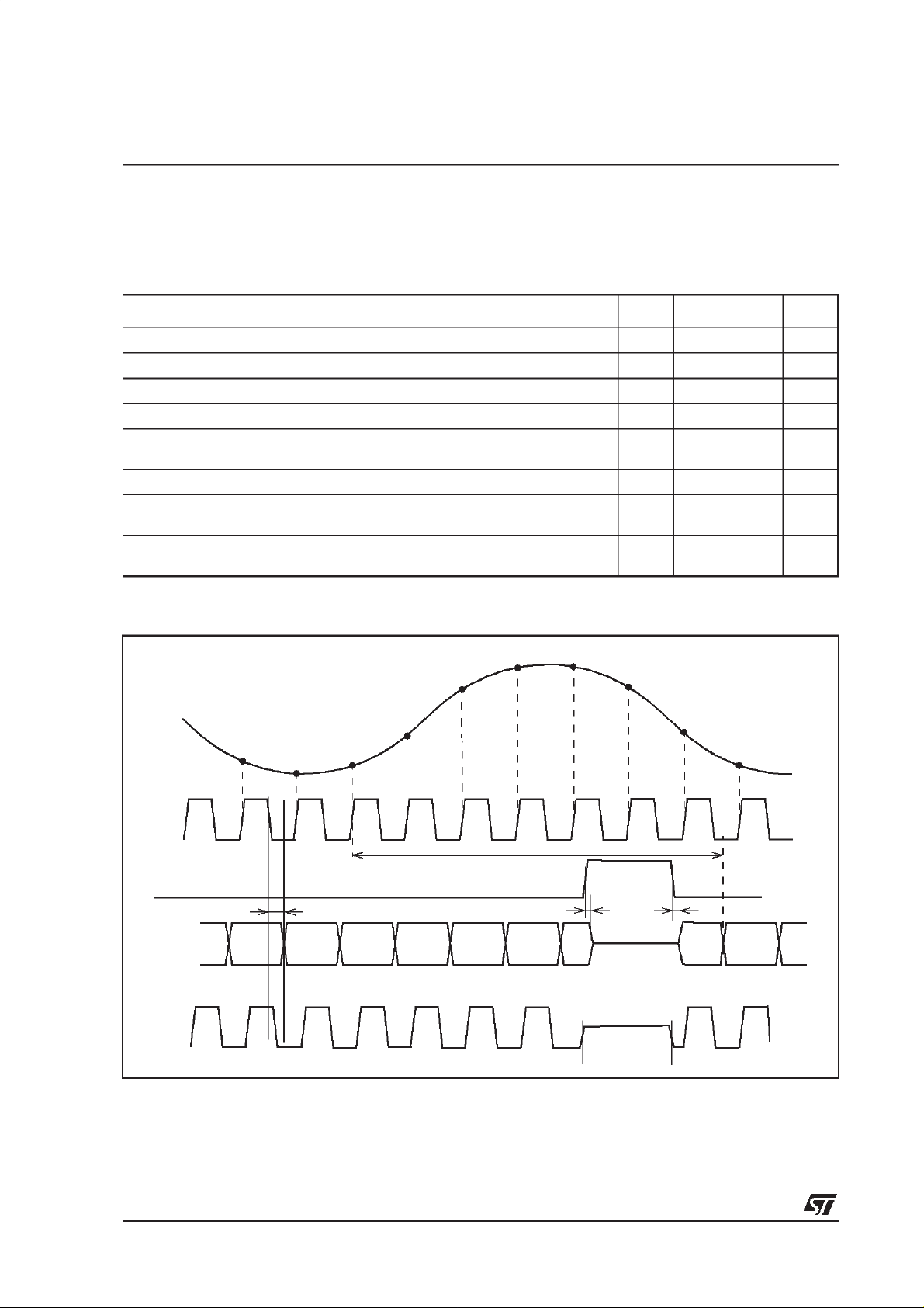
TIMING DIAGRAM
N-1
CLK
OEB
Tod
DATA
OUT
DR
N-8
N+4
N+3
N+2
N-7
N+1
6.5 clk cycles
N-5N-6
N-4
N-3
N
Toff
N+5
N-2
N+6
N+7
N+8
Ton
N
N+1
HZstate
4/20
TSA0801
CONDITIONS
AVCC = DVCC = VCCB = 2.5V, Fs= 40Msps,Fin= 1MHz, Vin@ -1.0dBFS, VREFM= 0V
Tamb = 25°C (unless otherwise specified)
ANALOG INPUTS
Symbol Parameter Test conditions Min Typ Max Unit
VIN-VINB Full scale reference voltage 2.0 Vpp
Cin Input capacitance 7.0 pF
BW Analog Input Bandwitdh Vin@-1dBFS, FS=40Msps 100 MHz
ERB
1) See parameters definition for more information
Effective Resolution Bandwidth
1)
REFERENCE VOLTAGE
Symbol Parameter Test conditions Min Typ Max Unit
60 MHz
VREFP Top internal reference voltage
Tmin= -40°C to Tmax= 85°C
Vpol Analog bias voltage
Tmin= -40°C to Tmax= 85°C
Ipol Analog bias current Normal operating mode 50 70 100 µA
Ipol Analog bias current Shutdown mode 0 µA
VINCM Input common mode voltage
Tmin= -40°C to Tmax= 85°C
1) Not fully tested over the temperature range. Guaranted by sampling.
1)
1)
1)
0.89 1.03 1.16 V
0.88 1.16 V
1.19 1.27 1.35 V
1.18 1.36 V
0.46 0.57 0.66 V
0.46 0.66 V
5/20
TSA0801
CONDITIONS
AVCC = DVCC = VCCB = 2.5V, Fs=40Msps, Fin= 1MHz, Vin@ -1.0dBFS, VREFP=1V, VREFM= 0V
Tamb = 25°C (unless otherwise specified)
POWER CONSUMPTION
Symbol Parameter Test conditions Min Typ Max Unit
1)
ICCA Analog Supply current
Tmin= -40°C to Tmax= 85°C
1)
ICCD Digital Supply Current
Tmin= -40°C to Tmax= 85°C
1)
ICCB Digital Buffer Supply Current
Tmin= -40°C to Tmax= 85°C
ICCBZ
PdZ
Rthja
Rthjc
1) Rpol= 18K
2) Not fully tested over the temperature range. Guaranted by sampling.
Digital Buffer Supply Current in
High Impedance Mode
Power consumption in normal
Pd
operation mode
Power consumption in High
Impedance mode
Junction-ambient thermal resis-
tor (TQFP48)
Junction-case thermal resistor
(TQFP48)
Ω.
Equivalent load: Rload= 470Ω and Cload= 6pF
1)
1)
Tmin= -40°C to Tmax= 85°C
1)
DIGITALINPUTS AND OUTPUTS
15.8 20 mA
2)
21 mA
1.3 2 mA
2)
2mA
2.1 5 mA
2)
5mA
50 110 µA
48 60 mW
2)
62 mW
43 55 mW
80 °C/W
18 °C/W
Symbol Parameter Test conditions Min Typ Max Unit
Digital inputs
VIL Logic ”0” voltage 0.8 V
VIH Logic ”1” voltage 2.0 V
Digital Outputs
VOL Logic ”0” voltage Iol=10µA 0.4 V
VOH Logic ”1” voltage Ioh=10µA 2.4 V
IOZ High Impedance leakage current OEB set to VIH -1.5 1.5 µA
C
Output Load Capacitance 15 pF
L
ACCURACY
Symbol Parameter Test conditions Min Typ Max Unit
OE Offset Error mV
DNL Differential Non Linearity -0.5 +0.5 LSB
INL Integral Non Linearity -1 +1 LSB
Monotonicity and no missing
6/20
codes
Guaranted
 Loading...