TS971
TS972
TS974
OUTPUT RAIL TO RAIL
VERYLOW NOISE OPERATIONAL AMPLIFIERS
.
RAILTO RAIL OUTPUT VOLTAGESWING
(±2.4V @ V
.
VERYLOW NOISE LEVEL: 4nV/√√Hz
.
ULTRALOWDISTORTION : 0.003%
.
HIGHDYNAMIC FEATURES(12MHz, 4V/µs)
.
OPERATINGRANGE : 2.7Vto 12V
.
ESD PROTECTION(2kV)
.
LATCH-UP IMMUNITY
.
AVAILABLEIN SOT23-5 MICROPACKAGE
= ±2.5V)
CC
DESCRIPTION
The TS97x family operational amplifiers is able to
operate with voltages as low as ±1.35Vandfeaturing output Rail to Rail signal swing. The TS97x
boasts characteristics that make them particularly
well suited for portableandbattery-suppliedequipment. Very low noise and low distortion characteristics make them ideal for audio
pre-amplification.
The TS971 is housed in the space-saving 5 pins
SOT23 package which simplifies theboard design
because of the ability to be placed everywhere
(outside dimensionsare 2.8mmx 2.9mm)
APPLICATIONS
.
Portableequipments(CD players, PDA)
.
Portablecommunications (cellphones, pagers)
.
Instrumentation& sensoring
.
Professionalaudio circuits
PIN CONNECTIONS (top view)
TS971ILT
Output
1
V
2
DD
Non-inverting input
Non-inve rting Input 1
Inve rting Inp ut 1
Non -inverting Input 1
3
TS971ID
1
N.C.
Inverting Inpu t1
Output1
2
-
+
3
V
4
DD
TS972IN-TS972ID-TS972IPT
1
-
2
+
3
V
45
DD
-
+
V
5
CC
Inverting input
4
N.C.
8
V
7
CC
6
Output 2
N.C.
5
V
8
CC
Output 2
7
6
Inve rting Input 2
Non-inverting Input2
ORDER CODES
Part
Number
TS971I -40, +125
TS972I -40, +125
TS974I -40, +125
N = Dual inLine Package (DIP)
D = Small Outline Package (SO) - also available in Tape & Reel
P = Thin Shrink Small Outline Package (TSSOP) - onlyavailable
in Tape & Reel (PT)
L = Tiny Package (SOT23-5) - only availablein Tape & Reel (LT)
August 1999
Temperature
Range
o
o
o
Package
NDPL
C ••K120
C •••
C •••
SOT23
Marking
TS974IN-TS974ID-TS974IPT
Output 1
1
Inverting Input 1
Non-invertingInput 1
Non-inverting Inp ut2
Inverting Input 2
V
Output 2
2
-
+
3
4
CC
5
+
-
6
7
14
13
-
+
12
11
10
+
-
9
8
Output 4
Inverting Input 4
Non-inverting Input4
V
DD
Non-inverting Input3
Inverting Input 3
Output 3
1/12

TS971-TS972-TS974
ABSOLUTEMAXIMUM RATINGS
Symbol Parameter Value Unit
V
CC
V
id
V
in
T
oper
T
stg
T
R
thjc
R
thja
ESD Human BodyModel 2 kV
Notes: 1. All voltages values, except differential voltage arewith respect to network ground terminal.
Supply Voltage - note 1 12 V
Differential Input Voltage - note2 ±V
CC
Input VoltageRange - note 3 -0.3 to12.3 V
Operating Free AirTemperature Range -40 to +125
Storage Temperature Range -65 to+150
Maximum JunctionTemperation 150
j
Thermal Resistance Junction to Case - note 4
SOT23-5
SO8
SO14
TSSOP8
TSSOP14
81
28
22
26
21
Thermal Resistance Junction to Ambient 256
Lead Temperature (soldering, 10sec) 260
2. Differential voltages are non-inverting input terminal with respect to the inverting input terminal.
3. The magniture of input and output voltages mustnever exceed V
4. Short-circuits can cause excessive heatingand destructive dissipation.
CC
+0.3V.
o
o
o
o
C/W
o
C/W
o
V
C
C
C
C
OPERATINGCONDITIONS
Symbol Parameter Value Unit
V
CC
V
icm
Supply Voltage Range 2.7 to 12 V
Common ModeInput VoltageRange VDD+ 1.15 to VCC- 1.15 V
2/12

TS971-TS972-TS974
ELECTRICAL CHARACTERISTICS
=2.5V,VDD= -2.5V, T
V
CC
Symbol Parameter Min. Typ. Max. Unit
V
DV
V
io
I
io
I
ib
icm
Input OffsetVoltage
T
min.<Tamb<Tmax.
Input OffsetVoltage Drift
io
= 0V, Vo=0V 5
V
icm
Input OffsetCurrent
= 0V, Vo= 0V 10 150
V
icm
Input BiasCurrent
= 0V, Vo=0V
V
icm
T
min.<Tamb<Tmax.
Common ModeInput VoltageRange -1.35 ±1.5 1.35 V
CMR Common Mode Rejection Ratio
= ±1.35V 60 85
V
icm
SVR Supply Voltage Rejection Ratio
V
= ±2V to ±3V 60 70
CC
A
V
V
I
source
I
sink
I
CC
vd
OH
OL
Large Signal VoltageGain RL=2kΩ 70 80 dB
High Level Output Voltage RL=2kΩ 2 2.4 V
Low Level OutputVoltage RL=2kΩ -2.4 -2 V
Output Source Current 1.5 mA
Output SinkCurrent 100 mA
Supply Current
Unity gain - no load 2 2.8
GBP Gain Bandwidth Product
f = 100kHz R
SR Slew Rate
A
=1,Vin= ±1V 2.8 4
V
∅m Phase Margin atUnity Gain R
Gm Gain Margin R
e
n
THD
Equivalent Input Noise Voltage
f = 100kHz
Total Harmonic Distortion
f = 1kHz,A
=25oC (unless otherwisespecified)
amb
=2kΩ,CL= 100pF 8.5 12
L
=2kΩ,CL= 100pF 60 Degrees
L
=2kΩ,CL= 100pF 10 dB
L
=-1 RL=10kΩ 0.003
V
15
7
200
200
750
1000
4
mV
µV/
nA
nA
dB
dB
mA
MHz
V/µs
nV
√Hz
o
C
%
3/12

TS971-TS972-TS974
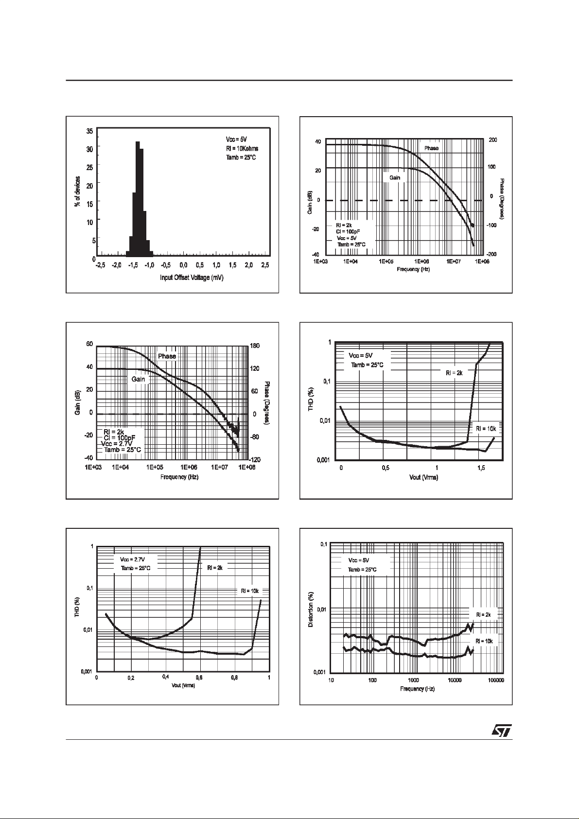
INPUT OFFSET VOLTAGEDISTRIBUTION
VOLTAGE GAIN & PHASEvs FREQUENCY
VOLTAGE GAIN& PHASE vs FREQUENCY
THDvs Vout
THD vs Vout THDvs FREQUENCY
4/12
 Loading...