


TS951
TS952
TS954
INPUT/OUTPUTRAIL TO RAIL
LOW POWER OPERATIONALAMPLIFIERS
August 1999
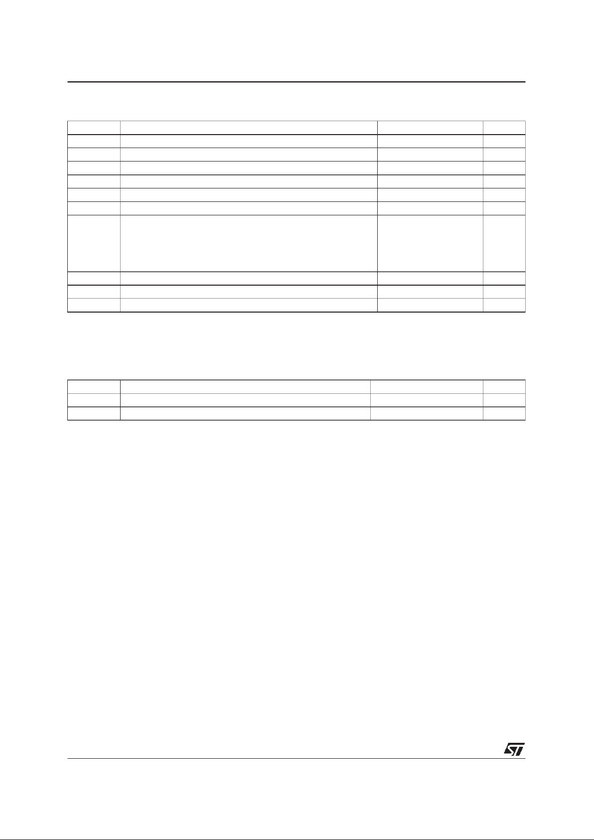
PIN CONNECTIONS (top view)
.
RAILTORAIL INPUT COMMON-MODE
VOLTAGERANGE
.
RAILTO RAIL OUTPUT VOLTAGESWING
.
OPERATINGFROM 2.7V to 12V
.
HIGHSPEED (3MHz, 1V/µs)
.
LOW CONSUMPTION (0.9mA@ 3V)
.
SUPPLYVOLTAGE REJECTIONRATIO : 80dB
.
ESD PROTECTION(2kV)
.
LATCH-UPIMMUNITY
.
AVAILABLEIN SOT23-5MICROPACKAGE
DESCRIPTION
The TS95x family are RAIL TO RAIL BiCMOS
operational amplifiersoptimizedandfully specified
for 3V and 5Voperation.
The TS951 is housed in the space-saving 5 pins
SOT23 package that makes it well suited for battery-powered systems. This micropackage simplifies the PC board design because of it’s ability to
be placed in tight spaces(outside dimensions are
: 2.8mm x 2.9mm)
APPLICATIONS
.
Set-topboxes
.
Laptop/Notebookcomputers
.
Transformer/Linedrivers
.
Personalentertainments(CD players)
.
Portablecommunication(cell phones, pagers)
.
Instrumentation& sensoring
.
Digitalto Analogconverter buffers
.
Portableheadphone speakerdrivers
ORDER CODES
Part
Number
Temperature
Range
Package
SOT23
Marking
NDPL
TS951I -40,+125
o
C ••K101
TS952I -40,+125
o
C •••
TS954I -40,+125
o
C •••
1
2
3
4
5
6
7
8
-
+
Inverting Input 1
N.C.
Non-inverting Input 1
V
DD
V
CC
Output 2
N.C.
N.C.
TS951ID
1
2
3
4
5
Inverting input
Non-inverting input
Output
V
DD
V
CC
TS951ILT
1
2
3
45
6
7
8
-
+
-
+
Inverting Input 1
Output 1
Non-inverting Input 1
V
DD
V
CC
Output 2
Inverting Input 2
Non-inverting Input 2
TS952IN-TS952ID-TS952IPT
Inverting Input 2
Non-inverting Input 2
Non-inverting Input 1
DD
V
1
2
3
4
8
5
6
7
9
10
11
12
13
14
CC
V
Output 3
Output 4
Non-inverting Input 4
Inverting Input 4
Non-inverting Input 3
Inverting Input 3
-
+
-
+
-
+
-
+
Output 1
Inverting Input 1
Output 2
TS954IN-TS954ID-TS954IPT
N = Dual inLine Package (DIP)
D = Small Outline Package (SO) - also available in Tape & Reel
P = Thin Shrink Small Outline Package (TSSOP) - only available
in Tape & Reel (PT)
L = Tiny Package (SOT23-5) - only available in Tape & Reel (LT)
1/13
ABSOLUTE MAXIMUM RATINGS
Symbol Parameter Value Unit
V
CC
Supply Voltage- note 1 12 V
V
id
Differential Input Voltage - note 2 ±1V
V
in
Input Voltage Range - note 3 -0.3 to 12.3 V
T
oper
Operating FreeAir Temperature Range -40 to +125
o
C
T
stg
Storage Temperature Range -65 to +150
o
C
T
j
Maximum Junction Temperation 150
o
C
R
thjc
Thermal Resistance Junction to Case -note 4
SOT23-5
SO8
SO14
TSSOP8
TSSOP14
81
28
22
26
21
o
C/W
R
thja
Thermal Resistance Junction to Ambient - SOT23-5 256
o
C/W
ESD Human Body Model 2 kV
Lead Temperature (soldering, 10sec) 260
o
C
Notes: 1. All voltages values, except differential voltage are with respect to network ground terminal.
2. Differential voltages are non-inverting input terminal with respect to the inverting input terminal.
3. The magnitude of input and output voltages must never exceed V
CC
+0.3V.
4. Short-circuits can cause excessive heatingand destructive dissipation.
OPERATING CONDITIONS
Symbol Parameter Value Unit
V
CC
Supply Voltage Range 2.7 to 12 V
V
icm
Common Mode Input VoltageRange VDD- 0.2 to VCC+ 0.2 V
TS951-TS952-TS954
2/13
ELECTRICAL CHARACTERISTICS
V
CC
=+3V,VDD= 0V,T
amb
=25oC (unlessotherwise specified)
Symbol Parameter Min. Typ. Max. Unit
V
io
Input Offset Voltage
T
min.
≤ T
amb
≤ T
max.
6
8
mV
DV
io
Input Offset Voltage Drift 2 µV/oC
I
io
Input Offset Current
T
min.
≤ T
amb
≤ T
max.
13080nA
I
ib
Input Bias Current
V
icm
= 1.5V
T
min.
≤ T
amb
≤ T
max.
35 100
200
nA
V
icm
Common Mode Input VoltageRange VDD- 0.2to VCC+ 0.2 V
CMR Common Mode Rejection Ratio 50 80 dB
SVR Supply Voltage Rejection Ratio
V
CC
= 2.7V to 3.3V 60 80
dB
A
vd
Large Signal Voltage Gain
V
o
= 2Vpk-pk RL= 600Ω 80
dB
V
OH
High Level Output Voltage RL= 600Ω 2.8 2.9 V
V
OL
Low Level Output Voltage RL= 600Ω 80 250 mV
I
sc
Output Short Circuit Current 10 mA
I
CC
Supply Current (peramplifier)
No load, V
o=VCC/2
0.9 1.3
mA
GBP Gain Bandwidth Product R
L
=2kΩ 3 MHz
SR Slew Rate 1 V/µs
∅m Phase Margin at Unity Gain R
L
= 600Ω,CL= 100pF 60 Degrees
G
m
Gain Margin RL= 600Ω,CL= 100pF 10 dB
e
n
Equivalent Input Noise Voltage
f = 1kHz 25
nV
√Hz
THD Total Harmonic Distortion
V
o
= 4Vpk-pk, f = 10kHz, AV=2,RL= 10kΩ 0.01
%
TS951-TS952-TS954
3/13
ELECTRICAL CHARACTERISTICS
V
CC
=+5V,VDD= 0V,T
amb
=25oC (unlessotherwise specified)
Symbol Parameter Min. Typ. Max. Unit
V
io
Input Offset Voltage
T
min.
≤ T
amb
≤ T
max.
6
8
mV
DV
io
Input Offset Voltage Drift 2 µV/oC
I
io
Input Offset Current
T
min.
≤ T
amb
≤ T
max.
13080nA
I
ib
Input Bias Current
V
icm
= 1.5V
T
min.
≤ T
amb
≤ T
max.
35 100
200
nA
V
icm
Common Mode Input VoltageRange VDD- 0.2to VCC+ 0.2 V
CMR Common Mode Rejection Ratio 50 80 dB
SVR Supply Voltage Rejection Ratio
V
CC
= 2.7V to 3.3V 60 80
dB
A
vd
Large Signal Voltage Gain
V
o
= 2Vpk-pk RL= 600Ω 86
dB
V
OH
High Level Output Voltage RL= 600Ω 4.7 4.8 V
V
OL
Low Level Output Voltage RL= 600Ω 80 300 mV
I
sc
Output Short Circuit Current 10 mA
I
CC
Supply Current (peramplifer)
No load, V
o=VCC/2
0.95 1.4
mA
GBP Gain Bandwidth Product R
L
=2kΩ 3 MHz
SR Slew Rate 1 V/µs
∅m Phase Margin at Unity Gain R
L
= 600Ω,CL= 100pF 60 Degrees
G
m
Gain Margin RL= 600Ω,CL= 100pF 10 dB
e
n
Equivalent Input Noise Voltage
f = 1kHz 25
nV
√Hz
THD Total Harmonic Distortion
V
o
= 4Vpk-pk, f = 10kHz, AV=2,RL= 10kΩ 0.01
%
TS951-TS952-TS954
4/13

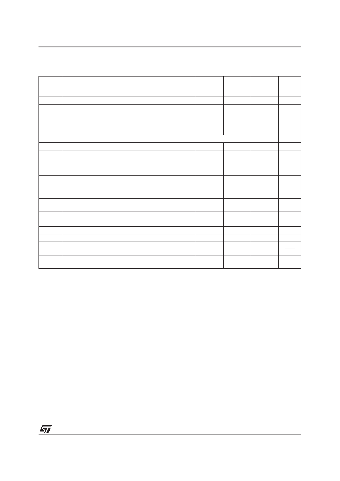
10
15
20
25
30
AmbientTemperature (°C)
Output short CircuitCurrent (mA)
-40 25 125
Vcc=0/5V
source
sink
OUTPUT SHORTCIRCUIT CURRENT VERSUS
TEMPERATURE
VOLTAGE GAIN AND PHASE VERSUS
FREQUENCY
024681012
0
0,2
0,4
0,6
0,8
1
1,2
Supply Voltage (V)
Supply Current (mA)
no load
T=25°C
SUPPLY CURRENT VERSUSSUPPLY
VOLTAGE
0,6
0,7
0,8
0,9
1
1,1
Ambient Temperature(°C)
SupplyCurrent (mA)
-40 25 125
Vcc=0/5V
SUPPLYCURRENT VERSUSTEMPERATURE
-25
-20
-15
-10
-5
0
5
10
15
20
25
30
outputvoltage (V)
output short circuit current (mA)
0 0.4 .6 1.2 1.8 2.4 2.6 2.8 3
sink
source
Vcc=3V
T=25°C
OUTPUT SHORT CIRCUITCURRENT VERSUS
OUTPUT VOLTAGE
0,7
0,8
0,9
1
1,1
1,2
1,3
AmbientT emperature (°C)
Slew Rate (V/µs)
-40 25 125
Vcc=0/3V - Rl=10k
SR+
SR-
SLEWRATE VERSUSTEMPERATURE
TS951-TS952-TS954
5/13

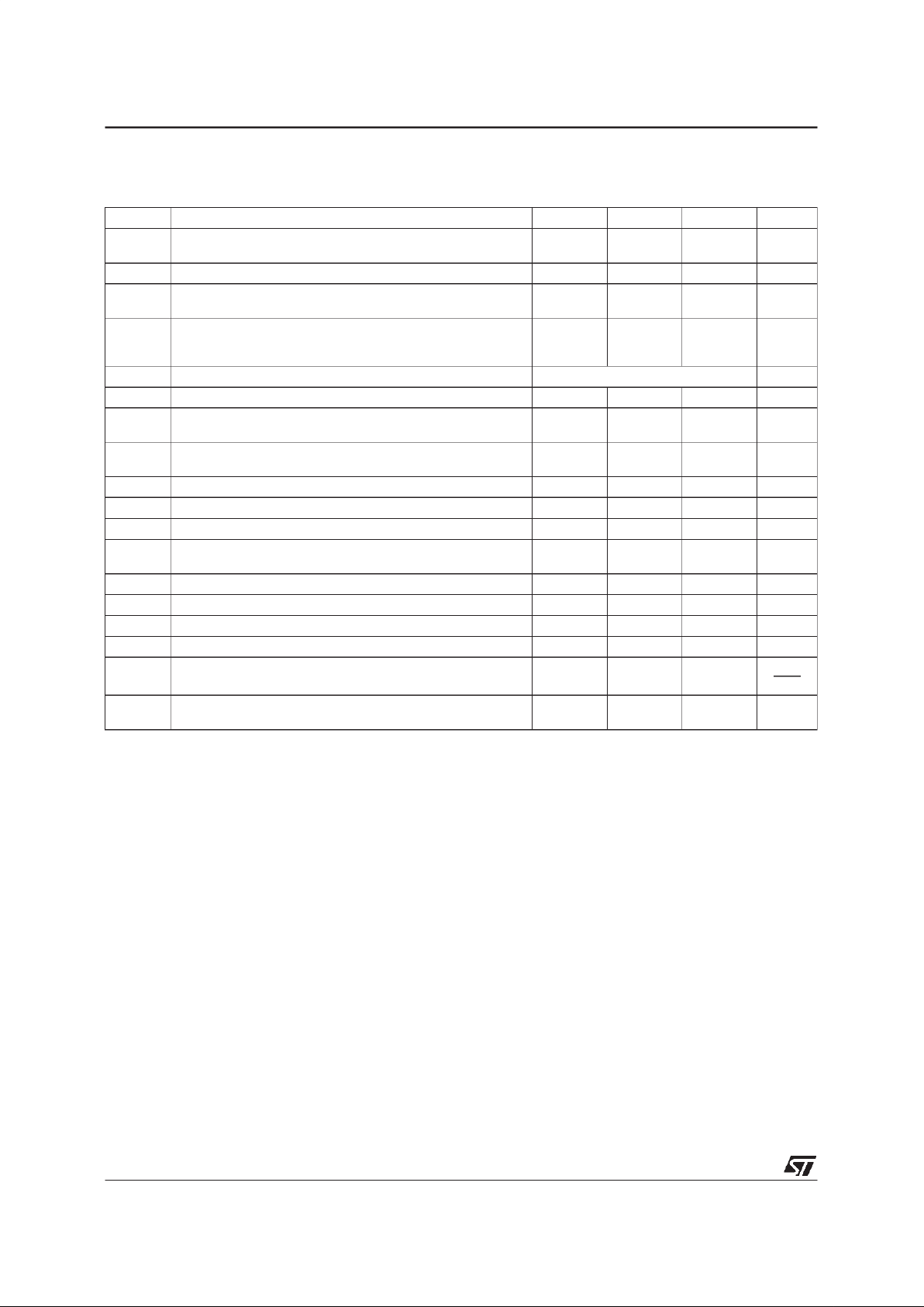
0 0,1 0,2 0,3 0,4 0,5 0,6 0,7 0,8 0,9 1 1,1
0,001
0,010
0,100
1,000
Vout(Vrms)
THD + Noise (%)
Vcc=+-1.5V
f=1kHz
G=-1
Rl=600ohms
THD + NOISE VERSUSV
out
0 0,1 0,2 0,3 0,4 0,5 0,6 0,7 0,8 0,9 1 1,1
0,001
0,010
0,100
1,000
Vout (Vrms)
THD + noise (%)
Vcc=+-1.5
f=1kHz
G=- 1
Rl=2k
THD + NOISE VERSUS V
out
10 100 1000 10000 100000
0
0,02
0,04
0,06
0,08
0,1
Frequency (Hz)
THD + Noise (%)
Vcc=+-1.5V
Rl=600ohms
Vo=2Vpp
THD + NOISE VERSUSFREQUENCY EQUIVALENTINPUT NOISE VOLTAGE
VERSUSFREQUENCY
TS951-TS952-TS954
6/13

Dimensions
Millimeters Inches
Min. Typ. Max. Min. Typ. Max.
A 3.32 0.131
a1 0.51 0.020
B 1.15 1.65 0.045 0.065
b 0.356 0.55 0.014 0.022
b1 0.204 0.304 0.008 0.012
D 10.92 0.430
E 7.95 9.75 0.313 0.384
e 2.54 0.100
e3 7.62 0.300
e4 7.62 0.300
F 6.6 0260
i 5.08 0.200
L 3.18 3.81 0.125 0.150
Z 1.52 0.060
PACKAGEMECHANICAL DATA
8 PINS- PLASTICPACKAGE
TS952IN
TS951-TS952-TS954
7/13

Dim.
Millimeters Inches
Min. Typ. Max. Min. Typ. Max.
A 1.75 0.069
a1 0.1 0.25 0.004 0.010
a2 1.65 0.065
a3 0.65 0.85 0.026 0.033
b 0.35 0.48 0.014 0.019
b1 0.19 0.25 0.007 0.010
C 0.25 0.5 0.010 0.020
c1 45
o
(typ.)
D 4.8 5.0 0.189 0.197
E 5.8 6.2 0.228 0.244
e 1.27 0.050
e3 3.81 0.150
F 3.8 4.0 0.150 0.157
L 0.4 1.27 0.016 0.050
M 0.6 0.024
S8
o
(max.)
PACKAGEMECHANICAL DATA
8 PINS- PLASTICMICROPACKAGE (SO)
TS951ID-TS952ID
TS951-TS952-TS954
8/13

PACKAGEMECHANICAL DATA
8 PINS- THINSHRINK SMALL OUTLINE PACKAGE
Dim.
Millimeters Inches
Min. Typ. Max. Min. Typ. Max.
A 1.20 0.05
A1 0.05 0.15 0.01 0.006
A2 0.80 1.00 1.05 0.031 0.039 0.041
b 0.19 0.30 0.007 0.15
c 0.09 0.20 0.003 0.012
D 2.90 3.00 3.10 0.114 0.118 0.122
E 6.40 0.252
E1 4.30 4.40 4.50 0.169 0.173 0.177
e 0.65 0.025
k0
o
8
o
0
o
8
o
l 0.50 0.60 0.75 0.09 0.0236 0.030
TS952IPT
TS951-TS952-TS954
9/13

Dim.
Millimeters Inches
Min. Typ. Max. Min. Typ. Max.
a1 0.51 0.020
B 1.39 1.65 0.055 0.065
b 0.5 0.020
b1 0.25 0.010
D 20 0.787
E 8.5 0.335
e 2.54 0.100
e3 15.24 0.600
F 7.1 0.280
i 5.1 0.201
L 3.3 0.130
Z 1.27 2.54 0.050 0.100
PACKAGEMECHANICAL DATA
14 PINS- PLASTIC PACKAGE
TS954IN
TS951-TS952-TS954
10/13

Dim.
Millimeters Inches
Min. Typ. Max. Min. Typ. Max.
A 1.75 0.069
a1 0.1 0.2 0.004 0.008
a2 1.6 0.063
b 0.35 0.46 0.014 0.018
b1 0.19 0.25 0.007 0.010
C 0.5 0.020
c1 45
o
(typ.)
D 8.55 8.75 0.336 0.334
E 5.8 6.2 0.228 0.244
e 1.27 0.050
e3 7.62 0.300
F 3.8 4.0 0.150 0.157
G 4.6 5.3 0.181 0.208
L 0.5 1.27 0.020 0.050
M 0.68 0.027
S8
o
(max.)
PACKAGEMECHANICAL DATA
14 PINS- PLASTIC MICROPACKAGE(SO)
TS954ID
TS951-TS952-TS954
11/13

PACKAGEMECHANICAL DATA
14 PINS- THIN SHRINK SMALL OUTLINEPACKAGE
Dim.
Millimeters Inches
Min. Typ. Max. Min. Typ. Max.
A 1.20 0.05
A1 0.05 0.15 0.01 0.006
A2 0.80 1.00 1.05 0.031 0.039 0.041
b 0.19 0.30 0.007 0.15
c 0.09 0.20 0.003 0.012
D 4.90 5.00 5.10 0.192 0.196 0.20
E 6.40 0.252
E1 4.30 4.40 4.50 0.169 0.173 0.177
e 0.65 0.025
k0
o
8
o
0
o
8
o
l 0.50 0.60 0.75 0.09 0.0236 0.030
TS954IPT
TS951-TS952-TS954
12/13

Information furnished is believed to be accurate and reliable. However, STMicroelectronics assumes no responsibility for the
consequences of use of such information nor for any infringement of patents orother rights of third parties which may result from
its use. No license is granted by implication or otherwiseunder any patent or patent rights of STMicroelectronics. Specifications
mentioned in this publication are subject to change without notice. This publication supersedes and replaces all information
previously supplied.STMicroelectronicsproductsarenotauthorized for use as criticalcomponentsin life support devicesor systems
without express written approval of STMicroelectronics.
The ST logo is a trademark of STMicroelectronics
1999 STMicroelectronics – Printed in Italy – All Rights Reserved
STMicroelectronics GROUP OF COMPANIES
Australia - Brazil - China - Finland - France - Germany - Hong Kong - India - Italy - Japan- Malaysia - Malta - Morocco
Singapore - Spain - Sweden - Switzerland - United Kingdom - U.S.A.
http://www.st.com
Dim.
Millimeters Inches
Min. Max. Min. Max.
A 0.90 1.45 0.034 0.057
A1 0 0.15 0.006
A2 0.90 1.30 0.034 0.051
b 0.35 0.50 0.013 0.020
C 0.09 0.20 0.003 0.008
D 2.80 3.00 0.110 0.118
E 2.60 3.00 0.102 0.118
E1 1.50 1.75 0.059 0.069
L 0.10 0.60 0.003 0.024
L
C
E1
A2
A
A1
b
E
D
PACKAGE MECHANICAL DATA
5 PINS-TINYPACKAGE(SOT23)
TS951ILT
TS951-TS952-TS954
13/13
 Loading...