

SGS Thomson Microelectronics TS954, TS952IN, TS952ID, TS952AIN, TS952AID Datasheet
...
TS951
TS952
TS954
INPUT/OUTPUTRAIL TO RAIL
LOW POWER OPERATIONALAMPLIFIERS
August 1999
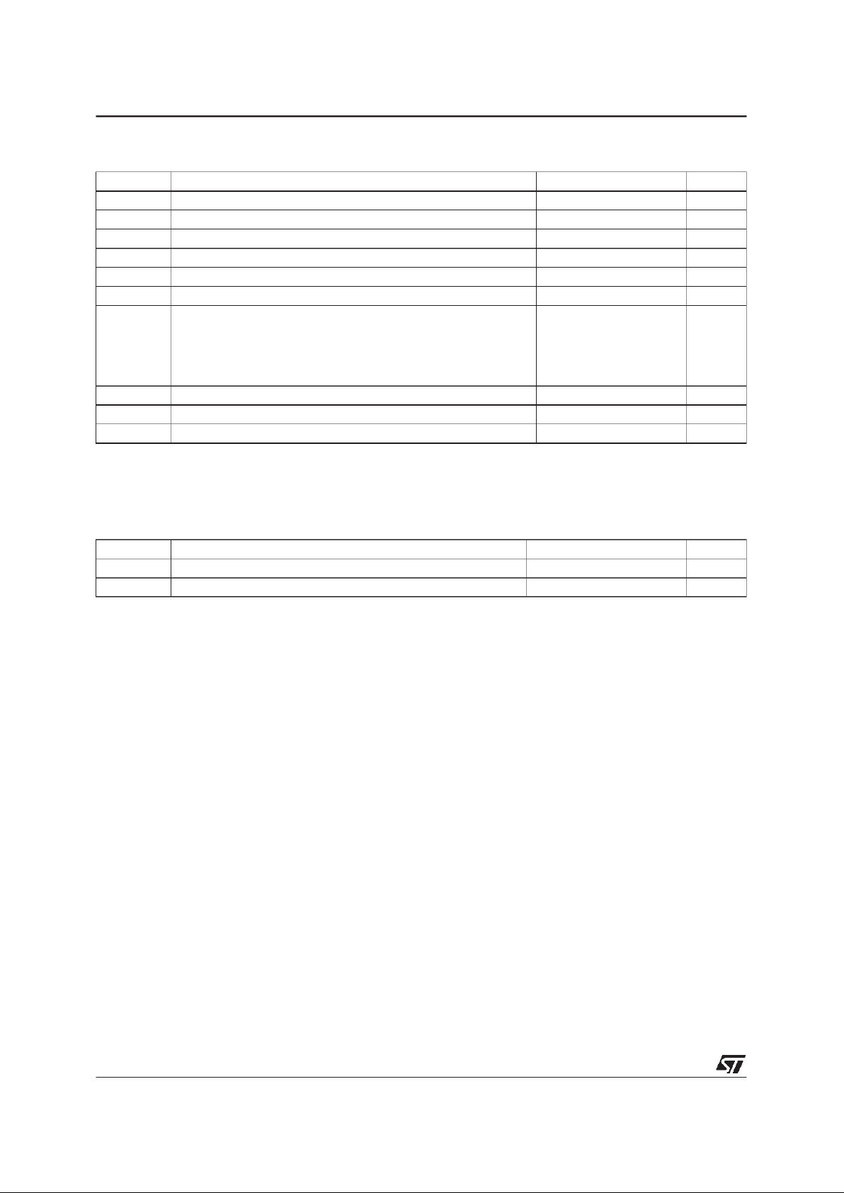
PIN CONNECTIONS (top view)
.
RAILTORAIL INPUT COMMON-MODE
VOLTAGERANGE
.
RAILTO RAIL OUTPUT VOLTAGESWING
.
OPERATINGFROM 2.7V to 12V
.
HIGHSPEED (3MHz, 1V/µs)
.
LOW CONSUMPTION (0.9mA@ 3V)
.
SUPPLYVOLTAGE REJECTIONRATIO : 80dB
.
ESD PROTECTION(2kV)
.
LATCH-UPIMMUNITY
.
AVAILABLEIN SOT23-5MICROPACKAGE
DESCRIPTION
The TS95x family are RAIL TO RAIL BiCMOS
operational amplifiersoptimizedandfully specified
for 3V and 5Voperation.
The TS951 is housed in the space-saving 5 pins
SOT23 package that makes it well suited for battery-powered systems. This micropackage simplifies the PC board design because of it’s ability to
be placed in tight spaces(outside dimensions are
: 2.8mm x 2.9mm)
APPLICATIONS
.
Set-topboxes
.
Laptop/Notebookcomputers
.
Transformer/Linedrivers
.
Personalentertainments(CD players)
.
Portablecommunication(cell phones, pagers)
.
Instrumentation& sensoring
.
Digitalto Analogconverter buffers
.
Portableheadphone speakerdrivers
ORDER CODES
Part
Number
Temperature
Range
Package
SOT23
Marking
NDPL
TS951I -40,+125
o
C ••K101
TS952I -40,+125
o
C •••
TS954I -40,+125
o
C •••
1
2
3
4
5
6
7
8
-
+
Inverting Input 1
N.C.
Non-inverting Input 1
V
DD
V
CC
Output 2
N.C.
N.C.
TS951ID
1
2
3
4
5
Inverting input
Non-inverting input
Output
V
DD
V
CC
TS951ILT
1
2
3
45
6
7
8
-
+
-
+
Inverting Input 1
Output 1
Non-inverting Input 1
V
DD
V
CC
Output 2
Inverting Input 2
Non-inverting Input 2
TS952IN-TS952ID-TS952IPT
Inverting Input 2
Non-inverting Input 2
Non-inverting Input 1
DD
V
1
2
3
4
8
5
6
7
9
10
11
12
13
14
CC
V
Output 3
Output 4
Non-inverting Input 4
Inverting Input 4
Non-inverting Input 3
Inverting Input 3
-
+
-
+
-
+
-
+
Output 1
Inverting Input 1
Output 2
TS954IN-TS954ID-TS954IPT
N = Dual inLine Package (DIP)
D = Small Outline Package (SO) - also available in Tape & Reel
P = Thin Shrink Small Outline Package (TSSOP) - only available
in Tape & Reel (PT)
L = Tiny Package (SOT23-5) - only available in Tape & Reel (LT)
1/13
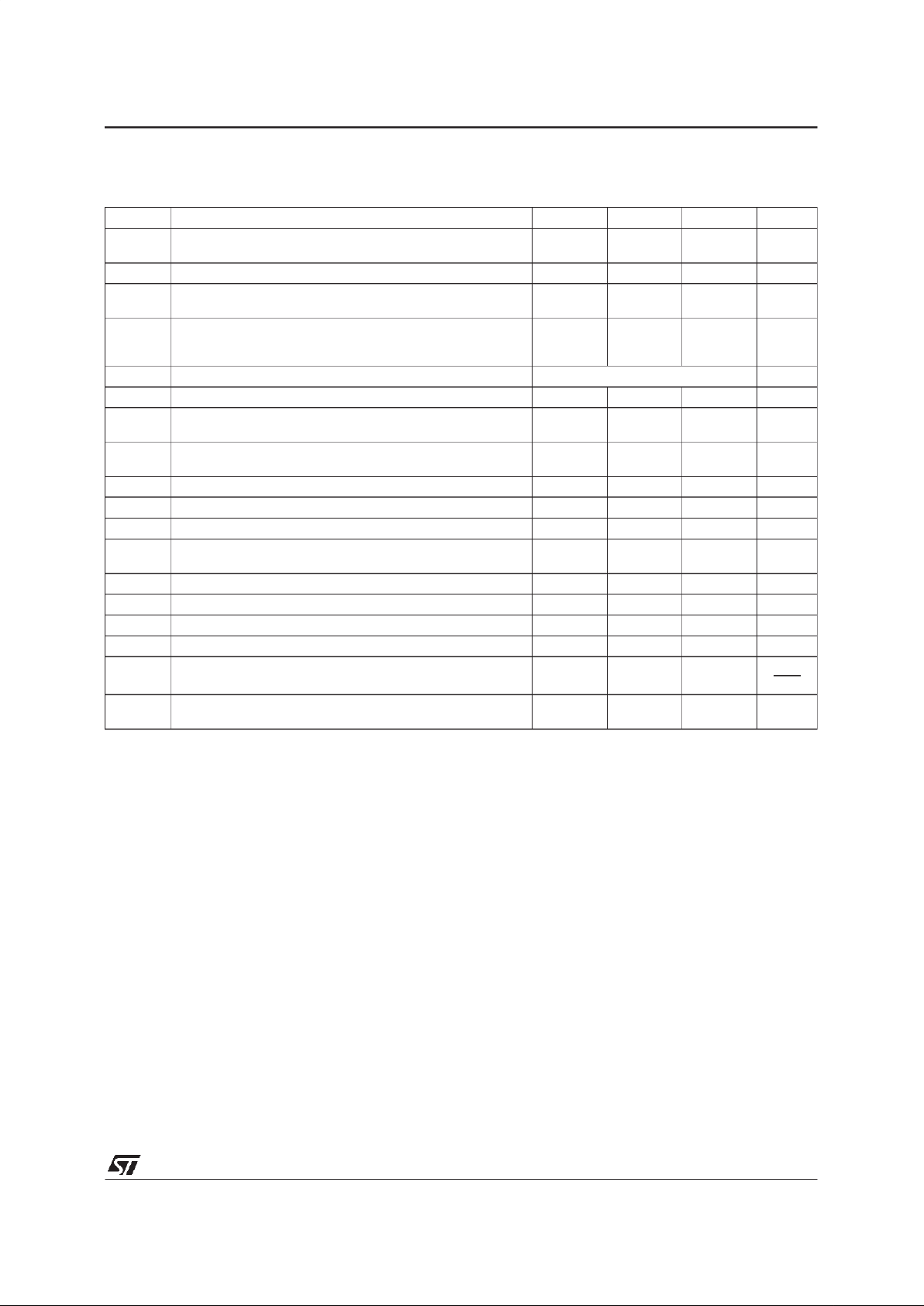
ABSOLUTE MAXIMUM RATINGS
Symbol Parameter Value Unit
V
CC
Supply Voltage- note 1 12 V
V
id
Differential Input Voltage - note 2 ±1V
V
in
Input Voltage Range - note 3 -0.3 to 12.3 V
T
oper
Operating FreeAir Temperature Range -40 to +125
o
C
T
stg
Storage Temperature Range -65 to +150
o
C
T
j
Maximum Junction Temperation 150
o
C
R
thjc
Thermal Resistance Junction to Case -note 4
SOT23-5
SO8
SO14
TSSOP8
TSSOP14
81
28
22
26
21
o
C/W
R
thja
Thermal Resistance Junction to Ambient - SOT23-5 256
o
C/W
ESD Human Body Model 2 kV
Lead Temperature (soldering, 10sec) 260
o
C
Notes: 1. All voltages values, except differential voltage are with respect to network ground terminal.
2. Differential voltages are non-inverting input terminal with respect to the inverting input terminal.
3. The magnitude of input and output voltages must never exceed V
CC
+0.3V.
4. Short-circuits can cause excessive heatingand destructive dissipation.
OPERATING CONDITIONS
Symbol Parameter Value Unit
V
CC
Supply Voltage Range 2.7 to 12 V
V
icm
Common Mode Input VoltageRange VDD- 0.2 to VCC+ 0.2 V
TS951-TS952-TS954
2/13
ELECTRICAL CHARACTERISTICS
V
CC
=+3V,VDD= 0V,T
amb
=25oC (unlessotherwise specified)
Symbol Parameter Min. Typ. Max. Unit
V
io
Input Offset Voltage
T
min.
≤ T
amb
≤ T
max.
6
8
mV
DV
io
Input Offset Voltage Drift 2 µV/oC
I
io
Input Offset Current
T
min.
≤ T
amb
≤ T
max.
13080nA
I
ib
Input Bias Current
V
icm
= 1.5V
T
min.
≤ T
amb
≤ T
max.
35 100
200
nA
V
icm
Common Mode Input VoltageRange VDD- 0.2to VCC+ 0.2 V
CMR Common Mode Rejection Ratio 50 80 dB
SVR Supply Voltage Rejection Ratio
V
CC
= 2.7V to 3.3V 60 80
dB
A
vd
Large Signal Voltage Gain
V
o
= 2Vpk-pk RL= 600Ω 80
dB
V
OH
High Level Output Voltage RL= 600Ω 2.8 2.9 V
V
OL
Low Level Output Voltage RL= 600Ω 80 250 mV
I
sc
Output Short Circuit Current 10 mA
I
CC
Supply Current (peramplifier)
No load, V
o=VCC/2
0.9 1.3
mA
GBP Gain Bandwidth Product R
L
=2kΩ 3 MHz
SR Slew Rate 1 V/µs
∅m Phase Margin at Unity Gain R
L
= 600Ω,CL= 100pF 60 Degrees
G
m
Gain Margin RL= 600Ω,CL= 100pF 10 dB
e
n
Equivalent Input Noise Voltage
f = 1kHz 25
nV
√Hz
THD Total Harmonic Distortion
V
o
= 4Vpk-pk, f = 10kHz, AV=2,RL= 10kΩ 0.01
%
TS951-TS952-TS954
3/13
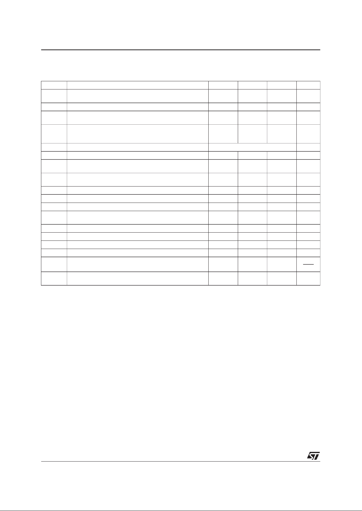
ELECTRICAL CHARACTERISTICS
V
CC
=+5V,VDD= 0V,T
amb
=25oC (unlessotherwise specified)
Symbol Parameter Min. Typ. Max. Unit
V
io
Input Offset Voltage
T
min.
≤ T
amb
≤ T
max.
6
8
mV
DV
io
Input Offset Voltage Drift 2 µV/oC
I
io
Input Offset Current
T
min.
≤ T
amb
≤ T
max.
13080nA
I
ib
Input Bias Current
V
icm
= 1.5V
T
min.
≤ T
amb
≤ T
max.
35 100
200
nA
V
icm
Common Mode Input VoltageRange VDD- 0.2to VCC+ 0.2 V
CMR Common Mode Rejection Ratio 50 80 dB
SVR Supply Voltage Rejection Ratio
V
CC
= 2.7V to 3.3V 60 80
dB
A
vd
Large Signal Voltage Gain
V
o
= 2Vpk-pk RL= 600Ω 86
dB
V
OH
High Level Output Voltage RL= 600Ω 4.7 4.8 V
V
OL
Low Level Output Voltage RL= 600Ω 80 300 mV
I
sc
Output Short Circuit Current 10 mA
I
CC
Supply Current (peramplifer)
No load, V
o=VCC/2
0.95 1.4
mA
GBP Gain Bandwidth Product R
L
=2kΩ 3 MHz
SR Slew Rate 1 V/µs
∅m Phase Margin at Unity Gain R
L
= 600Ω,CL= 100pF 60 Degrees
G
m
Gain Margin RL= 600Ω,CL= 100pF 10 dB
e
n
Equivalent Input Noise Voltage
f = 1kHz 25
nV
√Hz
THD Total Harmonic Distortion
V
o
= 4Vpk-pk, f = 10kHz, AV=2,RL= 10kΩ 0.01
%
TS951-TS952-TS954
4/13
 Loading...