

SGS Thomson Microelectronics TS944IN, TS944IDT, TS944ID, TS944BIN, TS944BID Datasheet
...
TS941
TS942
TS944
OUTPUT RAIL TO RAIL
MICROPOWER OPERATIONAL AMPLIFIERS
■ RAIL TO RAIL OUTPUT VOLTAGE SWING
■ MICROPOWER CONSUMPTION (1.2µA)
■ SINGLE SUPPLY OPERATION (2.7V to 10V)
■ CMOS INPUTS
■ ULTRA LOW INPUT BIAS CURRENT (1pA)
■ ESD PROTECTION (2kV)
■ LATCH-UP IMMUNITY (Class A)
■ AVAILABLE IN SOT23-5 MICROPACKAGE
DESCRIPTION
The TS94x (Single, Dual & Quad) is Operational
Amplifier characterized for 2.7V to 10V operation
over -40°C to +85°C temperature range.
It is exhibiting an excellent consumption - 1.2µA,
while featuring 10kHz gain bandwidth product,
1.5mA output capability and output Rail to Rail operation - 2.85V typ @ 3V with RL=10kΩ.
The TS94x Op-Amp is ideal for battery-powered
systems, where very low supply current and output Rail to Rail are required. Its very low - 1pA typ
input bias current and constant supply current
over supply voltage enhance TS94x’s performance near the end of the life battery charge.
APPLICATION
■ Battery-powered systems (Alarm)
■ Portable communication systems (Pagers)
■ Smoke/gas/fire detectors
■ Instrumentation & sensoring
■ PH Meter
ORDER CODE
PIN CONNECTIONS (top view)
TS941ILT
Output
1
V
2
DD
Non-inverting input
Inve rting Input 1
Non-inve rting Inp ut 1
TS942IN-TS942ID-TS942IDT-TS942IPT
Output 1
Inve rting Input 1
Non-inve rting Input 1
3
TS941ID-TS941IDT
1
N.C.
2
-
+
3
V
4
DD
1
-
2
+
3
V
45
DD
-
+
V
5
CC
Inverting input
4
N.C.
8
V
7
CC
6
Output 2
N.C.
5
V
8
CC
Output 2
7
Inverting Input 2
6
Non-inve rting Input 2
Part
Number
Temperature
Range
TS941I
TS941AI
-40, +85°C
TS941BI
TS942I
TS942AI
-40, +85°C••
TS942BI
TS944I
TS944AI
-40, +85°C••
TS944BI
N=Dual in Line Package (DIP)
D=Small Outline Package (SO) - also available in Tape & Reel (DT)
P=Thin Shrink Small Outline Package (TSSOP) - only available
in Tape & Reel (PT)
L=Tiny Package (SOT23-5) - only available in Tape & Reel (LT)
Package
NDPL
•
•
•
•
•
•
•
•
•
•
•
•
•
•
•
•
•
•
•
•
SOT23
Marking
K201
K202
K203
May 2000
TS944IN-TS944ID-TS944IDT-TS944IPT
14
13
+
12
11
10
+
-
9
8
Outp ut 4
Inverting Input 4
Non-inve rting Input4
V
DD
Non-inve rting Input3
Inverting Input 3
Outp ut 3
Output 1
Inve rting Input 1
Non-inve rting Input1
V
Non-inve rting Input 2
Inverting Input 2
Output 2
1
2
-
+
3
4
CC
5
+
-
6
7
1/14

TS941-TS942-TS944
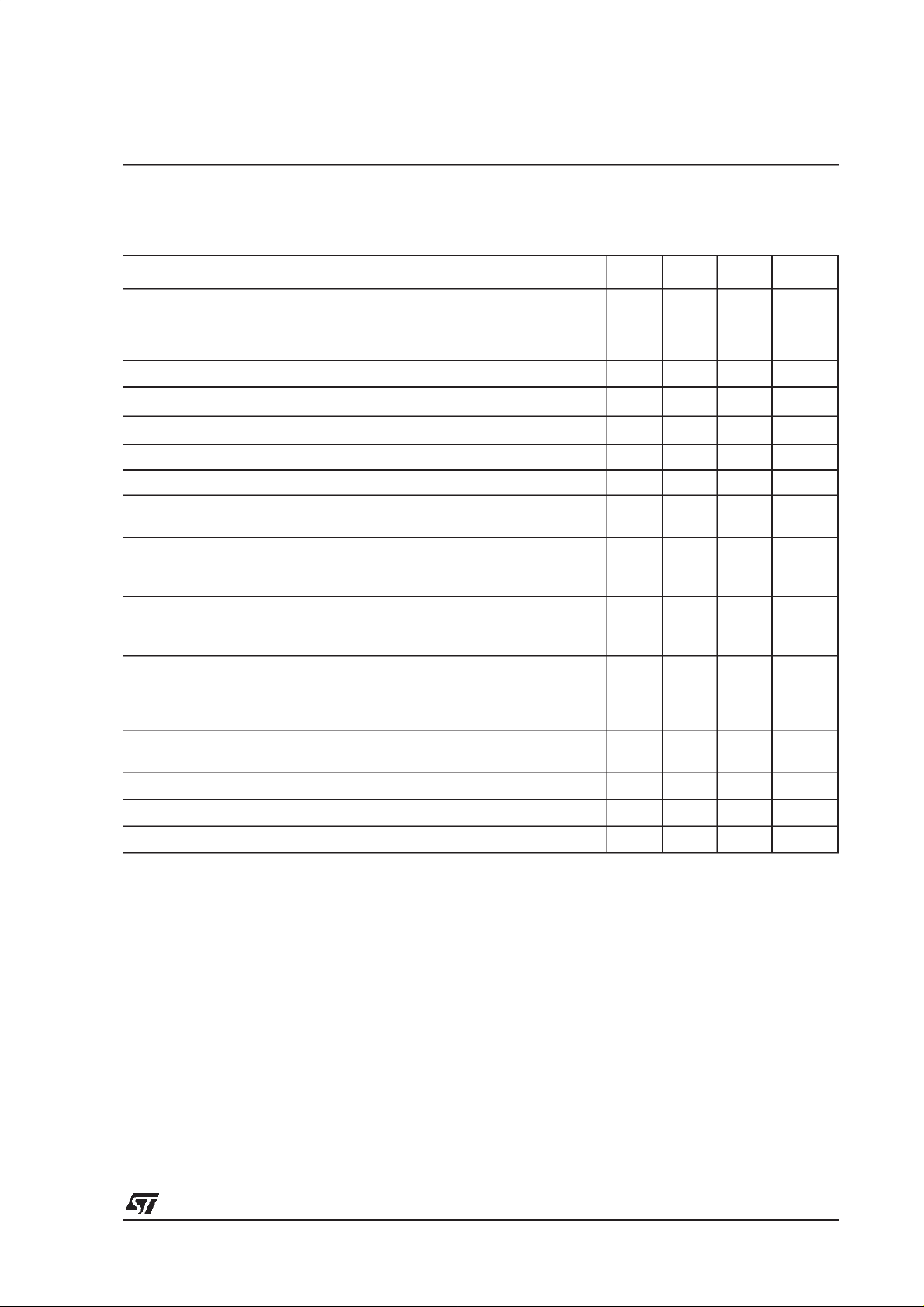
ABSOLUTE MAXIMUM RATINGS
Symbol Parameter Value Unit
V
T
T
R
Supply voltage
CC
V
Differential Input Voltage
id
V
in Input Voltage Range
Operating Free Air Temperature Range -40 to + 85 °C
oper
Storage Temperature Range -65 to +150 °C
std
T
Maximum Junction Temperature 150 °C
j
Thermal Resistance Junction to Case
thjc
SOT23-5
DIP8
DIP14
SO8
SO14
TSSOP8
TSSOP14
R
Thermal Resistance Junction to Ambient - SOT23-5 256 °C/W
thja
ESD Human Body Model 2 kV
Latch-up Immunity Class A
Lead Temperature (soldering, 10sec) 260 °C
1. All voltages values, except differential voltage are with respect to network terminal.
2. Differential voltages are non-inverting input terminal with respect to the inverting input terminal.
3. The magnitude of input and output voltages must never exceed V
4. Short-circuits can cause excessive heating and destructive dissipation.
1)
2)
3)
4)
12 V
±12 V
-0.3 to 12.3 V
81
42
32
28
22
26
21
+0.3V.
CC
°C/W
OPERATING CONDITIONS
Symbol Parameter Value Unit
V
V
Supply Voltage 2.7 to 10 V
CC
Common Mode Input Voltage Range
icm
V
CC
-
-0.2 to V
CC
+
-1.3
V
2/14
TS941-TS942-TS944
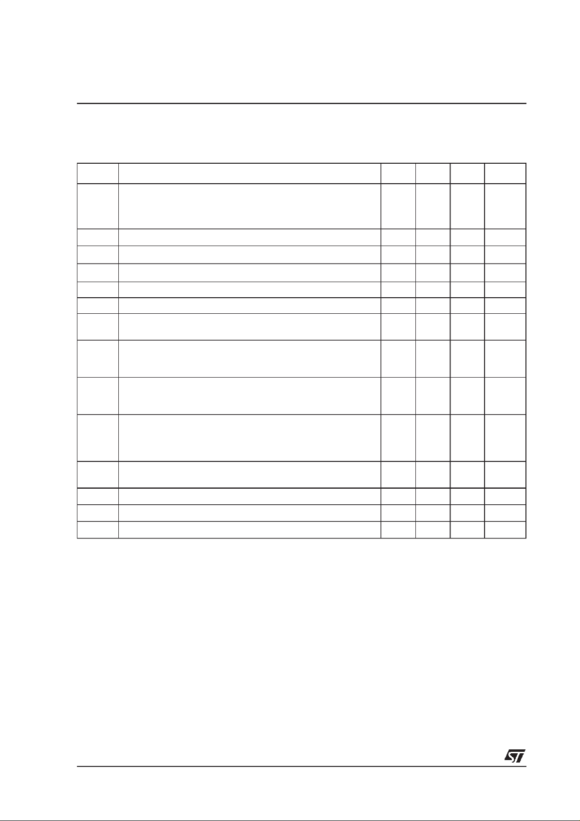
ELECTRICAL CHARACTERISTICS
VCC= +3V,Vee= 0V,RLconnected to V
T
=25°C (unless otherwise specified)
amb
Symbol Parameter Min. Typ. Max. Unit
Input Offset Voltage
V
io
∆V
CMR Common Mode Rejection Ratio 85 dB
SVR Supply Voltage Rejection Ratio 85 dB
V
V
GBP
1. Maximum values including unavoidable inaccurates of the industrial test.
Input Offset Voltage Drift 7 µV/°C
io
I
Input Offset Current
io
I
ib Input Bias Current
Large Signal Voltage Gain
A
vd
V
= 2Vpp RL=1MΩ
O
1)
1)
High Level Output Voltage
V
= 100mV RL=1MΩ
OH
ID
Low Level Output Voltage
V
= -100mV RL=1MΩ
OL
ID
Output Source Current
V
= 100mV, VO=V
I
o
Output Sink Current
Supply Current (per amplifier)
I
CC
ID
V
= -100mV,VO=V
ID
A
= 1, no load
VCL
DD
CC
Gain Bandwith Product R
Slew Rate R
SR
Phase Margin C
φm
,
CC/2
TS941/2/4
TS941/2/4A
TS941/2/4B
= 10kΩ
R
L
= 10kΩ
R
L
=1MΩ,CL= 50pF
L
=1MΩ,CL= 50pF
L
= 50pF
L
2.9
2.79
10
5
2
1 100 pA
1 150 pA
100
2.99
2.85
5
100
50
210
1.5
1.3
1.2 2
10 kHz
4 V/ms
65 Degrees
mV
dB
V
mV
mA
µA
3/14
TS941-TS942-TS944
ELECTRICAL CHARACTERISTICS
VCC= +5V,Vee= 0V,RLconnected to V
T
=25°C (unless otherwise specified)
amb
Symbol Parameter Min. Typ. Max. Unit
Input Offset Voltage
V
io
∆V
CMR Common Mode Rejection Ratio 85 dB
SVR Supply Voltage Rejection Ratio 85 dB
V
V
GBP
1. Maximum values including unavoidable inaccurates of the industrial test.
Input Offset Voltage Drift 7 µV/°C
io
I
io Input Offset Current
I
ib Input Bias Current
Large Signal Voltage Gain
A
vd
V
= 2Vpp RL=1MΩ
O
1)
1)
High Level Output Voltage
V
= 100mV RL=1MΩ
OH
ID
Low Level Output Voltage
V
= -100mV RL=1MΩ
OL
ID
Output Source Current
V
= 100mV, VO=V
I
o
Output Sink Current
Supply Current (per amplifier)
I
CC
ID
V
= -100mV,VO=V
ID
A
= 1, no load
VCL
DD
CC
Gain Bandwith Product R
Slew Rate R
SR
Phase Margin C
φm
,
CC/2
TS941/2/4
TS941/2/4A
TS941/2/4B
= 10kΩ
R
L
= 10kΩ
R
L
=1MΩ,CL= 50pF
L
=1MΩ,CL= 50pF
L
= 50pF
L
4.9
4.79
10
5
2
1 100 pA
1 150 pA
100
4.99
4.85
5
100
5
6
1.2 2
10 kHz
5 V/ms
65 Degrees
mV
dB
V
mV
mA
µA
4/14

TS941-TS942-TS944
Input Offset Voltage Drift vs Temperature
400
300
200
100
-100
-200
-300
-400
Input Offset Voltage Drift (µV)
-500
Supply Current/Amplifier vs Supply Voltage
1.5
1.0
Vcc = 3V & 5V
0
-40 -20 0 20 40 60 80
Temperature(°C)
in Overdrive
Tamb = 25°C
Vid = - 100mV
Vid= + 100mV
Supply Current/Amplifier vs Supply Voltage
2.0
Tamb = 25°C
1.5
1.0
Supply Current (µA)
0.5
0.0
0246810
Supply Voltage (V)
SupplyCurrent/Amplifiervs Temperature
1.30
1.25
Vcc from 2.6V to 10V
1.20
0.5
SupplyCurrent (µA)
0.0
0246810
Supply Voltage (V)
Output Short-Circuit Current vs Temperature
6
4
2
0
-2
-4
Output Short-circuit Current (mA)
-6
-40 -20 0 20 40 60 80
Temperature (°C)
Isink, Vcc=5V
Isink, Vcc=3V
Isource,Vcc=3V
Isource, Vcc=5V
Supply Current (µA)
1.15
1.10
-40 -20 0 20 40 60 80
Temperature(°C)
Output Short-Circuit Current vs
30
Tamb = 25°C
20
10
0
-10
-20
OutputShort-Circuit Current (mA)
-30
24 6810
SupplyVoltage
Sink
Source
Supply Voltage (V)
5/14
 Loading...