

SGS Thomson Microelectronics TS921IN, TS921ID, TS921 Datasheet
TS921
RAIL TO RAIL HIGH OUTPUT CURRENT
SINGLE OPERATIONALAMPLIFIER
March 1999
.
RAILTO RAIL INPUT AND OUTPUT
.
LOW NOISE : 9nV/√√((Hz))
.
LOW DISTORTION
.
HIGHOUTPUT CURRENT : 80mA
(able todrive 32Ω loads)
.
HIGHSPEED : 4MHz,1.3V/µs
.
OPERATINGFROM 2.7V to 12V
.
ESD INTERNALPROTECTION: 1.5KV
.
LATCH-UP IMMUNITY
.
MACROMODELINCLUDED IN THIS
SPECIFICATION
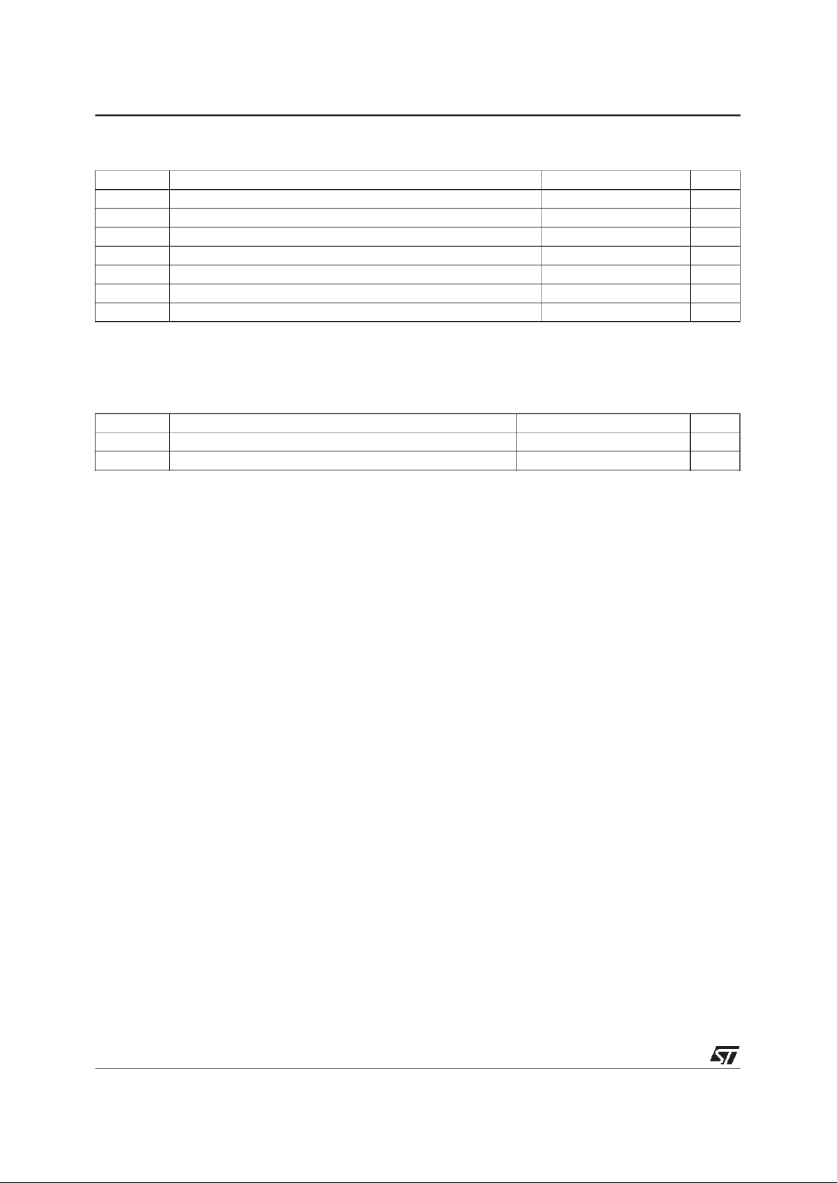
1
2
3
45
6
7
8
-
+
Inverting Input
N.C.
Non-inverting Input
V
CC
V
CC
+
Output
N.C.
N.C.
PIN CONNECTIONS (top view)
DESCRIPTION
The TS921is a RAILTO RAILsingle BiCMOS
operational amplifier optimized and fully specified
for 3V and 5V operation.
High outputcurrent allowslowload impedancesto
be driven.
The TS921exhibitsa verylownoise,lowdistortion,
low offsetand high ouput currentcapabilitymaking
this devicean excellent choicefor high quality,low
voltage or battery operated audio systems.
The device is stable for capacitive loads up to
500pF.
APPLICATIONS
.
headphoneamplifier
.
piezoelectricspeakerdriver
.
soundcards, multimedia systems
.
line driver, actuatordriver
.
servo amplifier
.
mobile phone and portablecommunication
sets
.
instrumentationwith low noise as a key factor
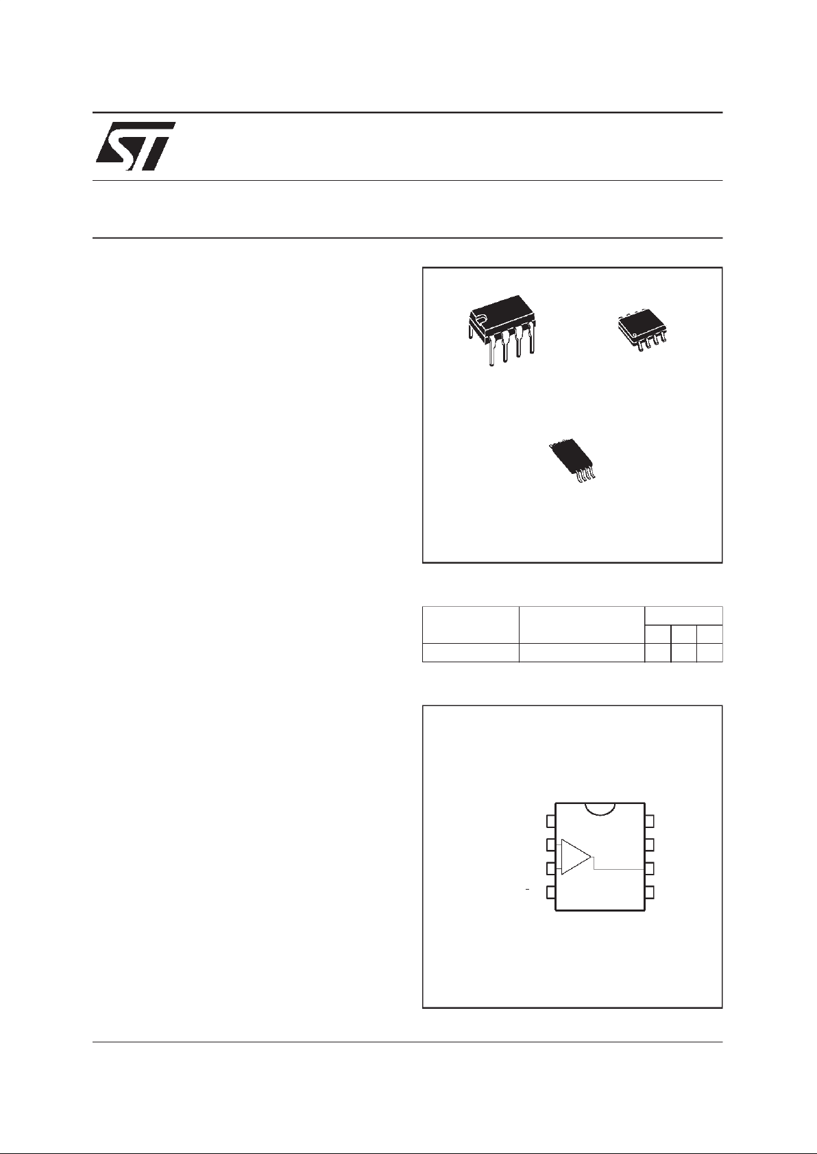
ORDER CODES
Part Number Temperature Range
Package
NDP
TS921I -40, +125
o
C •••
N
DIP8
(Plastic Package)
D
SO8
(Plastic Micropackage)
P
TSSOP8
(Thin Shrink Small Outline Package)
1/11
ABSOLUTEMAXIMUMRATINGS
Symbol Parameter Value Unit
V
CC
Supply Voltage - (note 1) 12 V
V
id
Differential Input Voltage - (note 2) ±1V
V
i
Input Voltage - (note 3) -0.3 to 14 V
T
oper
Operating Free Air Temperature Range -40 to +125
o
C
T
stg
Storage Temperature -65 to +150
o
C
T
j
Maximum Junction Temperature 150
o
C
Output Short Circuit Duration see note 4
o
C
Notes : 1. All voltage values, except differentialvoltage are with respect to networkground terminal.
2. Differential voltages are the non-inverting input terminal with respect to the inverting input terminal.
3. The magnitude of input and output voltages must never exceed V
CC
+
+0.3V.
4. Short-circuits can cause excessive heating.
OPERATINGCONDITIONS
Symbol Parameter Value Unit
V
CC
Supply Voltage 2.7to 12 V
V
icm
Common Mode Input Voltage Range V
CC
-
-0.2 to V
CC
+
+0.2 V
TS921
2/11
ELECTRICAL CHARACTERISTICS
V
CC
+
=3V,T
amb
=25oC (unless otherwisespecified)
Symbol Parameter Min. Typ. Max. Unit
V
io
InputOffset Voltage
T
min.
≤ T
amb
≤ T
max.
3
5
mV
DV
io
InputOffset Voltage Drift 2 µV/oC
I
io
InputOffset Current
V
out
= 1.5V 30
nA
I
ib
InputBias Current
V
out
= 1.5V 15 100
nA
V
OH
HighLevel Output Voltage RL= 600Ω
R
L
=32Ω
2.87
2.63
V
V
OL
Low Level Output Voltage RL= 600Ω
R
L
=32Ω 180
100 mV
A
vd
LargeSignal Voltage Gain (V
out
= 2Vpk-pk) RL= 600Ω
R
L
=32Ω
35
16
V/mV
I
CC
SupplyCurrent
no load, V
out=VCC/2
1 1.5
mA
GBP Gain Bandwidth Product
R
L
= 600Ω 4
MHz
CMR Common Mode Rejection Ratio 60 80 dB
SVR Supply Voltage Rejection Ratio
V
CC
= 2.7 to 3.3V 60 80
dB
I
o
Output Short Circuit Current 50 80 mA
SR Slew Rate 0.7 1.3 V/µs
∅m PhaseMargin at Unity Gain
R
L
= 600Ω,CL= 100pF 68
Degrees
G
m
Gain Margin
R
L
= 600Ω,CL= 100pF 12
dB
e
n
Equivalent Input Noise Voltage
f = 1kHz
9
nV
√Hz
THD Total Harmonic Distortion
V
out
= 2Vpk-pk, F = 1kHz, AV=1,RL= 600Ω 0.005
%
TS921
3/11
ELECTRICALCHARACTERISTICS
V
CC
+
=5V,T
amb
=25oC (unlessotherwise specified)
Symbol Parameter Min. Typ. Max. Unit
V
io
Input Offset Voltage
T
min.
≤ T
amb
≤ T
max.
3
5
mV
DV
io
Input Offset Voltage Drift 2 µV/oC
I
io
Input OffsetCurrent
V
out
= 1.5V 30
nA
I
ib
Input Bias Current
V
out
= 1.5V 15 100
nA
V
OH
High Level Output Voltage RL= 600Ω
R
L
=32Ω
4.85
4.4
V
V
OL
Low Level Output Voltage RL= 600Ω
R
L
=32Ω 300
120 mV
A
vd
Large Signal Voltage Gain (V
out
= 2Vpk-pk) RL= 600Ω
R
L
=32Ω
35
16
V/mV
I
CC
Supply Current
no load, V
out=VCC/2
1 1.5
mA
GBP Gain Bandwidth Product
R
L
= 600Ω 4
MHz
CMR Common Mode Rejection Ratio 60 80 dB
SVR Supply Voltage Rejection Ratio
V
CC
= 2.7 to 3.3V 60 80
dB
I
o
Output Short Circuit Current 50 80 mA
SR Slew Rate 0.7 1.3 V/µs
∅m Phase Margin at Unity Gain
R
L
= 600Ω,CL= 100pF 68
Degrees
G
m
Gain Margin
R
L
= 600Ω,CL= 100pF 12
dB
e
n
Equivalent Input Noise Voltage
f = 1kHz
9
nV
√Hz
THD Total Harmonic Distortion
V
out
= 2Vpk-pk, F = 1kHz, AV=1,RL= 600Ω 0.005
%
TS921
4/11
 Loading...