

SGS Thomson Microelectronics TS831-5IZ, TS831-5ID, TS831-5, TS831-4IZ, TS831-4IN Datasheet
...
1/11
■ ULTRA LOW POWER CONSUMPTION :
12µA maximum
■ PRECISION RESETTHRESHOLD
■ THRESHOLD VOLTAGE:
4.33V typ. FOR TS831-5
4.50V typ. FOR TS831-4
2.71V typ. FOR TS831-3
■ GUARANTEED RESET OPERATION FOR
VCC DOWN TO 1V
■ OPEN DRAIN OUTPUT COMPARATOR
■ FAST RESPONSE TIME : 20µs FOR A 10mV
OVERDRIVE
■ INTERNAL BUILT-IN HYSTERESIS
■ PIN TO PIN COMPATIBLEWITH MC33064
AND MC33164
DESCRIPTION
The TS831 ultra low power integrated circuit incorporates a high stability band-gap voltage reference and a comparator with open drain output.
The threshold voltage is set at 4.33V for TS831-5,
4.5V for TS831-4 and 2.71V for TS831-3 by internal thermally matched resistances.
The comparator exhibits a 20µs response (with
10mV overdrive) and has an open drain output active when input voltage is lower than the threshold.
An internal hysteresis, 100mV for TS831-4/
TS831-5 and 60mV for TS831-3, increases the
comparator’s noise margin and prevents false reset operation.
APPLICATION
■ Power-on reset generator for microcontroller
■ Power failure detector
ORDER CODE
Z= TO92 Plastic package
D=Small Outline Package (SO) - also available in Tape & Reel (DT)
P=Thin Shrink Small Outline Package (TSSOP) - only available
in Tape & Reel (PT)
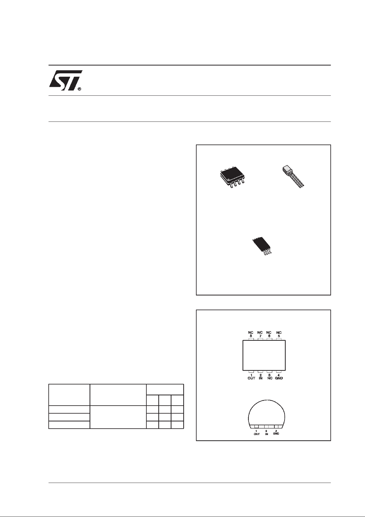
PIN CONNECTIONS (top view)
Part Number Temperature Range
Package
DZP
TS831-5I
-40, +125°C
•••
TS831-4I •••
TS831-3I •••
D
DIP-8
(Plastic Micropackage)
P
TSSOP-8
(Thin Shrink Small Outline Package)
Z
TO-92
(Plastic Package)
TO-92
SO8-TSSOP8
TS831
MICROPOWER VOLTAGE SUPERVISOR
RESET ACTIVE LOW
March 2000
TS831
2/11
ABSOLUTE MAXIMUM RATINGS
OPERATING CONDITIONS
TS831-5
ELECTRICAL CHARACTERISTICS Tamb = 25°C (unless otherwise specified)
Symbol Parameter Value Unit
V
CC
Supply Voltage
1)
7V
V
out
Output Voltage
-0.3 to V
cc
+ 0.3
V
I
out
Output Sink Current TS831-5 and TS831-4
TS831-3
20
5
mA
Pd
Power Dissipation
2)
TO-92
SO-8
TSSOP-8
625
700
625
mW
I
F
Clamp Diode Forward Current, pin 1 to pin 2
3)
100 mA
T
oper
Operating Free Air Temperature Range -40 to +85 °C
T
stg
Storage Temperature -65 to +150 °C
1. All voltages values, except differential voltage are with respect to network ground terminal.
2. T
j
= 150°C, T
amb
=25oC with Rthja = 200oC/W for TO-92 package
Rthja = 175
o
C/W for SO8 package
Rthja = 200
o
C/W for TSSOP8 package
3. Maximum package power dissipation limits must be observed.
Symbol Parameter Value Unit
V
CC
Supply Voltage 1 to 5.5 V
Symbol Parameter Min. Typ. Max. Unit
V
thi
Threshold Voltage - VCCIncreasing
-40°C ≤ Tamb ≤ +85°C
-40°C ≤ Tamb ≤ +125°C
4.10
4.10
4.33
4.46
4.50
V
V
thd
Threshold Voltage - VCCDecreasing
-40°C ≤ Tamb ≤ +85°C
-40°C ≤ Tamb ≤ +125°C
4.10
4.06
4.21
4.46
4.46
V
V
hys
Hysteresis Voltage 50 100 200 mV
I
CC
Current Consumption VCC=5V
12 µA
V
OL
Low Level Output Voltage VCC=4V,IOL= 8mA
-40°C ≤ Tamb ≤ +85°C
-40°C ≤ Tamb ≤ +125°C
450 800
1000
1300
mV
I
OH
Low Level Output Voltage VCC=5V
-40°C ≤ Tamb ≤ +125°C
2 100
1000
nA
tphl
Response Time High to Low
R
L
= 10kΩ,CL= 15pF,VCC=V
thd
-10mV
20 µs
Note : Limits are 100% production tested at 25°C. Limits over temperature are guaranteed through correlation and by design.
TS831
3/11
TS831-4
ELECTRICAL CHARACTERISTICS Tamb = 25°C (unless otherwise specified)
TS831-3
ELECTRICAL CHARACTERISTICS Tamb = 25°C (unless otherwise specified)
Symbol Parameter Min. Typ. Max. Unit
V
thi
Threshold Voltage - VCCIncreasing
-40°C ≤ Tamb ≤ +85°C
-40°C ≤ Tamb ≤ +125°C
4.17
4.10
4.35
4.66
4.70
V
V
thd
Threshold Voltage - VCCDecreasing
-40°C ≤ Tamb ≤ +85°C
-40°C ≤ Tamb ≤ +125°C
4.17
4.13
4.4
4.66
4.66
V
V
hys
Hysteresis Voltage 50 100 200 mV
I
CC
Current Consumption VCC=5V
12 µA
V
OL
Low Level Output Voltage VCC=4V,IOL= 8mA
-40°C ≤ Tamb ≤ +85°C
-40°C ≤ Tamb ≤ +125°C
450 800
1000
1300
mV
I
OH
Low Level Output Voltage VCC=5V
-40°C ≤ Tamb ≤ +125°C
2 100
1000
nA
tphl
Response Time High to Low
R
L
= 10kΩ,CL= 15pF,VCC=V
thd
-10mV
20 µs
Note : Limits are 100% production tested at 25°C. Limits over temperature are guaranteed through correlation and by design.
Symbol Parameter Min. Typ. Max. Unit
V
thi
Threshold Voltage - VCCIncreasing
-40°C ≤ Tamb ≤ +125°C
2.55
2.71
2.8
V
V
thd
Threshold Voltage - VCCDecreasing
-40°C ≤ Tamb ≤ +125°C
2.55
2.65
2.8
V
V
hys
Hysteresis Voltage 30 60 100 mV
I
CC
Current Consumption VCC=3V
12 µA
V
OL
Low Level Output Voltage VCC= 2.4V,IOL= 1mA
-40°C ≤ Tamb ≤ +125°C
140 400
500
mV
I
OH
Low Level Output Voltage VCC=3V
-40°C ≤ Tamb ≤ +125°C
2 100
1000
nA
tphl
Response Time High to Low
R
L
= 10kΩ,CL= 15pF,VCC=V
thd
-10mV
20 µs
Note : Limits are 100% production tested at 25°C. Limits over temperature are guaranteed through correlation and by design.
TS831
4/11
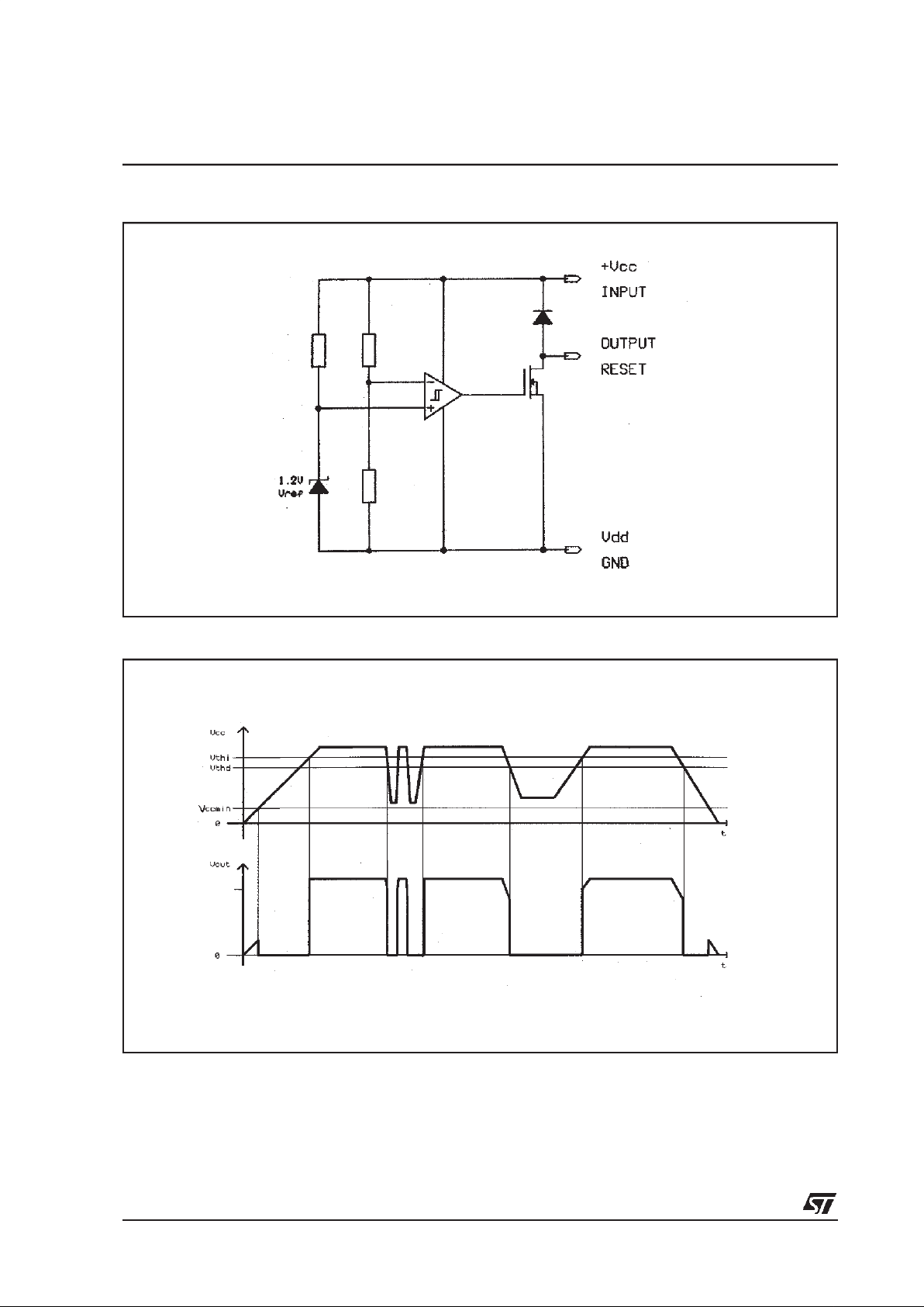
EQUIVALENT SCHEMATIC DIAGRAM
TIMING DIAGRAM

TS831
5/11
Output voltageversus input voltage
Output voltage versus input voltage
Output voltageversus input voltage
Reset output voltage versus Input voltage
Reset output voltage versus Input voltage
Reset output voltage versus Input voltage
0246810
Input voltage (V)
0
2
4
6
8
10
Output voltage (V)
TS831-3
R
L
= 10 Kohms
T=25°C
0246810
Input voltage (V)
0
2
4
6
8
10
Output voltage (V)
TS831-4
R
L= 10 Kohms
T=25°C
0246810
Input voltage (V)
0
2
4
6
8
10
Output voltage(V)
TS831-5
R
L
= 10 Kohms
T=25°C
2.60 2.65 2.70 2.75
Input voltage (V)
0.0
1.0
2.0
3.0
4.0
5.0
Output voltage (V)
TS831-3
R
L= 10 Kohms
T=25°C
4.4 4.5 4.6
Input voltage (V)
0.0
1.0
2.0
3.0
4.0
5.0
Output voltage (V)
TS831-4
R
L
=10 Kohms
T=25°C
4.20 4.24 4.28 4.32 4.36 4.40
Inputvoltage(V)
0.0
1.0
2.0
3.0
4.0
5.0
Outputvoltage (V)
TS831-5
R
L
= 10 Kohms
T=25°C

TS831
6/11
VthversustemperaturewhileVcc increasing
Hysteresis voltage versus temperature
Supplycurrent vsinputvoltage &temperature
VthversustemperaturewhileVcc decreasing
Supply current versus temperature
Voltage output low vs Isink & temperature
-40 -20 0 20 40 60 80 100 120
Temperature (°C)
4.4
4.4
4.5
4.5
4.6
Vthi (Volts)
V
th
i
m
a
x
V
th
i
m
i
n
TS831-4
-40 -20 0 20 40 60 80 100 120
Temperature (°C)
80
100
120
140
160
Hysteresis(mV)
TS831-4
0246810
Input voltage (V)
0
4
8
12
16
Supply current (µA)
TS831-3
No Load
+125°C
-40°C
25°C
-40°C
-40 -20 0 20 40 60 80 100 120
Temperature (°C)
4.32
4.34
4.36
4.38
4.40
4.42
4.44
Vthd (Volts)
V
th
d
m
a
x
TS831-4
V
t
h
d
m
in
-40-200 20406080100120
Temperatu re ( ° C)
8.2
8.4
8.6
8.8
9.0
9.2
9.4
9.6
Supply current (µA)
Ic
c
max
Ic
c
mi
n
TS8 31- 4
No lo ad
02468
Isink (mA)
0
0.5
1
1.5
2
2.5
3
Vol (V)
-40°C
+25°C
+85°C
+125°C
TS831-3
Vin=2.4V

TS831
7/11
Supplycurrent vsinputvoltage &temperature
Supplycurrentvs inputvoltage&temperature
Clamp diode forward current versus voltage
Voltage output low vs Isink & temperature
Voltage output low vs Isink & temperature
Response time
0246810
Input voltage (V)
0
4
8
12
Supply current (µA)
TS831-4
No Load
+125°C
-40°C
25°C
25°C
-40°C
+125°C
0246810
Input voltage (V)
0
4
8
12
Supply current (µA)
TS831-5
No Load
+125°C
-40°C
25°C
25°C
-40°C
+125°C
0 0.5 1 1.5
Forward voltage (V)
0
20
40
60
80
100
Forward current (mA)
Vin= 0V
T=25°C
0 5 10 15 20
Isink(mA)
0
1
2
3
4
Vol (V)
-40°C
+25°C
+85°C
+125°C
TS831-4
Vin=4V
0 5 10 15 20
Isink(mA)
0
1
2
3
4
Vol(V)
-40°C
+25°C
+85°C
+125°C
TS831-5
Vin=4V
0 20406080100
Time (µs)
Input
signal
Reset
output
4V
5V
0V
TS831-4
R
L
= 10 Kohms
T=25°C
5V

TS831
8/11
Basic configuration
Powe r
Sup p ly
Microprocessor
circ u it
Reset
TS8 31
in
G
nd
Pullup
resistor
Special remarks
* Some microprocessor may integrate the pull up resistor.
* For the pull up resistor choice, pleaseuse thegraphs namme d”V oltage
output low vs Isink & t emperature” depending on TS831 versions.

TS831
9/11
PACKAGE MECHANICAL DATA
8 PINS - PLASTIC MICROPACKAGE (SO)
Dim.
Millimeters Inches
Min. Typ. Max. Min. Typ. Max.
A 1.75 0.069
a1 0.1 0.25 0.004 0.010
a2 1.65 0.065
a3 0.65 0.85 0.026 0.033
b 0.35 0.48 0.014 0.019
b1 0.19 0.25 0.007 0.010
C 0.25 0.5 0.010 0.020
c1 45° (typ.)
D 4.8 5.0 0.189 0.197
E 5.8 6.2 0.228 0.244
e 1.27 0.050
e3 3.81 0.150
F 3.8 4.0 0.150 0.157
L 0.4 1.27 0.016 0.050
M 0.6 0.024
S8°(max.)

TS831
10/11
PACKAGE MECHANICAL DATA
3 PINS - PLASTIC PACKAGE TO-92
Dim.
Millimeters Inches
Min Typ. Max. Min. Typ. Max.
L 1.27 0.05
B 3.2 3.7 4.2 0.126 0.1457 0.1654
O1 4.45 5.00 5.2 0.1752 0.1969 0.2047
C 4.58 5.03 5.33 0.1803 0.198 0.2098
K 12.7 0.5
O2 0.407 0.5 0.508 0.016 0.0197 0.02
a 0.35 0.0138

TS831
11/11
Information furnished is believed to be accurate and reliable. However, STMicroelectronics assumes no responsibility for the
consequences of use of such information nor for any infringement of patents or other rights of third parties which may result from
its use. No license is granted by implication or otherwise under any patent or patent rights of STMicroelectronics. Specifications
mentioned in this publication are subject to change without notice. This publ ication supersedes and replaces all information
previously supplied. STMicroelectronics products are not authorized for use as critical components in life support devices or
systems withou texpress written approval of STMicroelectronics.
The ST logo is a registered trademark of STMicroelectronics
2000 STMicroelectronics - Printed in Italy - All Rights Reserved
STMicroelectronics GROUP OF COMPANIES
Australia - Brazil - China - Finland - France - Germany - Hong Kong - India - Italy - Japan - Malaysia - Malta - Morocco
Singapore - Spain - Sweden - Switzerland - United Kingdom
http://www.st.com
PACKAGE MECHANICAL DATA
8 PINS - THIN SHRINK SMALL OUTLINE PACKAGE
Dim.
Millimeters Inches
Min. Typ. Max. Min. Typ. Max.
A 1.20 0.05
A1 0.05 0.15 0.01 0.006
A2 0.80 1.00 1.05 0.031 0.039 0.041
b 0.19 0.30 0.007 0.15
c 0.09 0.20 0.003 0.012
D 2.90 3.00 3.10 0.114 0.118 0.122
E 6.40 0.252
E1 4.30 4.40 4.50 0.169 0.173 0.177
e 0.65 0.025
k0° 8°0° 8°
l 0.50 0.60 0.75 0.09 0.0236 0.030
0,25 mm
.010 inch
GAGE PLANE
Caaa
C
PLANE
SEATING
EA
A2
A1
D
b
e
E1
L
k
c
14
85
PIN 1IDENTIFICATION
L1
 Loading...