

SGS Thomson Microelectronics TS7211BILT, TS7211AILT Datasheet
1/9
■ RAIL TO RAIL INPUTS
■ PUSH-PULL OUTPUT
■ SUPPLY OPERATION FROM 2.7V TO 10V
■ TYPICAL SUPPLY CURRENT: 6µA @ 5V
■ RESPONSE TIME OF 0. 5µs AT 5V
■ LOW INPUT CURRENT
■ ESD PROTECTION : 2KV (HBM) 2 00V (MM)
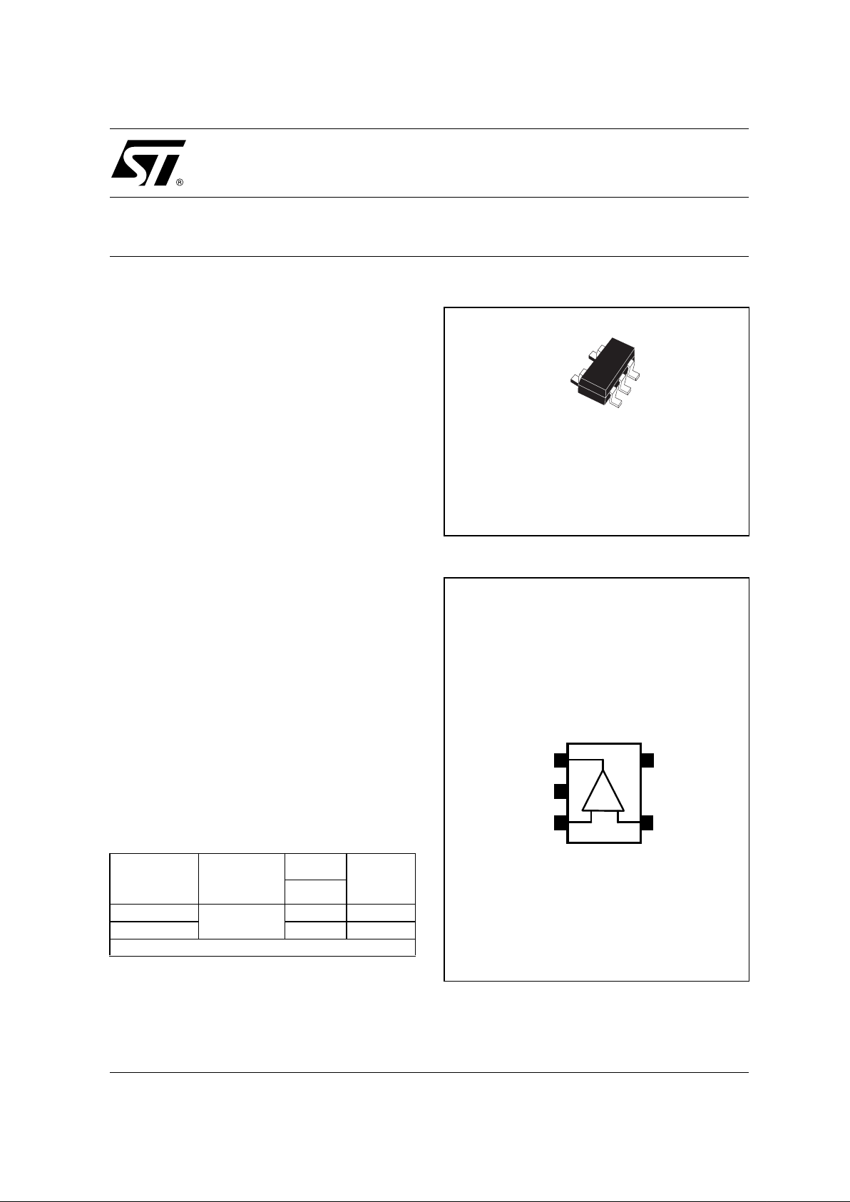
■ AVAILABLE IN TINY SOT23-5 PACKAGE
DESCRIPTION
The TS7211 is a micropower comparator
featuring rail to rail input performance in a tiny
SOT23-5 package. This comparator is ideally
suited to space and weight critical applications. It
is fully specified at 2.7V, 5V and 10V operations
over the industrial temperature range (-40/+85°C).
The TS7211 features a push-pull output stage.
The speed to power ratio mak es this device ultra
versatile for a wide range of applications.
APPLICATIONS
■ Battery powered systems
■ Notebooks and PDAs
■ PCMCIA cards
■ Cellulars and mobile communication
■ Alarm and security systems
■ Replacement of amplifiers used in
comparator configuration with better
performances
ORDER CODE
L = Tiny Package (SOT23-5) - only available in Tape & Reel (LT)
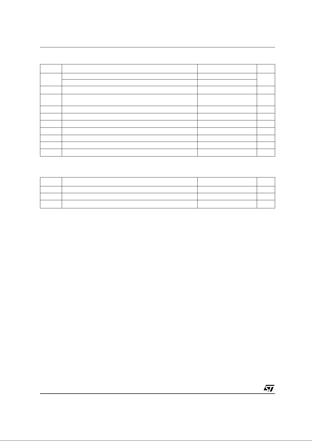
PIN CONNECTIONS (top view)
Part Number
Temperature
Range
Package
SOT23-5
Marking
L
TS7211AI
-40°C, +85°C
•
K515
TS7211BI
•
K516
Example : TS7211AILT
L
SOT23-5L
(Tiny Package)
TS7211 Push-Pull output
5
4
OUT
Vcc-
1
2
IN+
Vcc+
3
IN-
+
-
TS7211
SINGLE BiCMOS RAIL TO RAIL
µPOWER COMPARATOR
May 2002
TS7211
2/9
ABSOLUTE MAXIMUM RATINGS
OPERATING CONDITIONS
Symbol Parameter Value Unit
ESD
Human body model (HBM) 2000
V
Machine model (MM) 200
V
ID
Differential Input Voltage
(V
CC
-
) -0.3 to (V
CC
+
) +0.3
V
V
IN
&
V
OUT
Input and output Voltages
1)
(V
CC
-
) -0.3 to (V
CC
+
) +0.3
V
V
CC
Supply voltage 12 V
I
IN
Current at input pins ± 5 mA
I
OUT
Current at output pin ± 30 mA
T
Lead
Lead temperature (soldering 10 seconds) 250 °C
T
STG
Storage Temperature -65 to +150 °C
T
J
Junction Temperature 150 °C
P
D
Power dissipation 2) SOT23-5
500 mW
1. The magnitude of input and output voltages must never exceed 0.3V beyond the supply voltage.
2. T
J
= 150°C, T
AMB
= 25oC with R
TH-JA
= 250oC/W for SOT23-5 package
Symbol Parameter Value Unit
V
CC
Supply Voltage 2.7 to 10 V
T
AMB
Ambient Temperature -40 to +85 °C
V
ICM
Common mode input voltage range
(V
CC
-
) -0.3 to (V
CC
+
) +0.3
V
TS7211
3/9
ELECTRICAL CHARACTERISTICS
V
CC
+
= 2.7V, T
AMB
= 25°C (unless otherwise specified)
Symbol Parameter Min. Typ. Max. Unit
V
IO
Input Offset Voltage (Full common mode range)
TS7211A
T
MIN
≤ T
AMB
≤ T
MAX
TS7211B
T
MIN
≤ T
AMB
≤ T
MAX
7
10
15
18
mV
∆
V
IO
Input Offset Voltage Drift with temperature 6
µ
V/
o
C
I
IB
Input Bias Current
1)
T
MIN
≤ T
AMB
≤ T
MAX
1 300
600
pA
I
IO
Input Offset Current 1)
T
MIN
≤ T
AMB
≤ T
MAX
1 150
300
pA
CMRR
Common-mode Rejection Ratio (0 < V
icm
< 2.7V)
65 dB
PSRR
Power Supply Rejection Ratio (2.7 < V
CC
< 10V)
80 dB
A
VD Voltage Gain
2)
240 dB
V
ICM
Input Common Mode Voltage Range (upper rail)
T
MIN
≤ T
AMB
≤ T
MAX
3
2.7
V
Input Common Mode Voltage Range (lower rail)
T
MIN
≤ T
AMB
≤ T
MAX
-0.3
0.0
V
OH
High Level Output Voltage - I
source
= 2.5mA
T
MIN
≤ T
AMB
≤ T
MAX
2.35
2.15
2.45 V
V
OL
Low Level Output Voltage - I
sink
= 2.5mA
T
MIN
≤ T
AMB
≤ T
MAX
0.2 0.35
0.45
V
I
CC
Supply Current
No load, output low
No load, output high
6
8
12
14
µ
A
T
PLH
Response Time Low to High (Vic = 1.35V, CL = 50pF)
Overdrive = 10mV
Overdrive = 100mV
1.5
0.6
µ
s
T
PHL
Response Time Low to High (Vic = 1.35V, CL = 50pF)
Overdrive = 10mV
Overdrive = 100mV
1.5
0.5
µ
s
T
F
Fall Time (CL = 50pF)
Overdrive = 100mV
20 ns
T
R
Rise Time (CL = 50pF)
Overdrive = 100mV
20 ns
1) Maximum values include unavoidable inaccurates of the industrial test.
2) Design evaluation.
3) Limits are 100% production tested at +25°C. Limits over temperature are guaranteed through correlation and by design.
 Loading...