

SGS Thomson Microelectronics TS68HC901 Datasheet
HCMOS MULTI-FUNCTION PERIPHERAL
The TS68HC901 CMFP (CMOS Multi-Function
Peripheral) is acombination of many ofthe necessary peripheral functions in a microprocessor system.
Includedare :
.8 INPUT/OUTPUTPINS
• Individually programmable direction
• Individual interrupt sourcecapability
Programmable edgeselection
-
.16 SOURCEINTERRUPT CONTROLLER
• 8 Internalsources
• 8 Externalsources
• Individual source enable
• Individual source masking
• Programmable interrupt servicemodes
Polling
-
Vector generation
-
OptionalIn-servicestatus
-
• Daisy chaining capability
.FOUR TIMERS WITHINDIVIDUALLY
PROGRAMMABLE PRESCALING
• Two multimodetimers
Delay mode
-
Pulse widthmeasurement mode
-
Event counter mode
-
• Two delaymode timers
• Independent clock input
• Time outoutput option
.SINGLECHANNEL USART
• Full Duplex
• Asynchronous to65 kbps
• Bytesynchronous to1 Mbps
• Internal/External baud rate generation
• DMA handshake signals
• Modem control
• Loop backmode
.68000 BUSCOMPATIBLE
TS68HC901
48
PDIP48
1
PLCC52
(Ordering Information at the end of the Datasheet
DESCRIPTI ON
The use of the CMFP in a system can significantly
reduce chip count, thereby reducing system cost.
TheCMFPis completely68000bus compatible,and
24 directly addressable internal registers provide
thenecessary control andstatus interfacetotheprogrammer.
TheCMFP isa derivative of theMK3801 STI, aZ80
familyperipheral.
September1992
1/42
TS68HC901
INTRODUCTION
The TS68HC901 multi-function peripheral (CMFP)
is a member of the 68000 peripherals. The CMFP
directly interfaces to the 68000processor via anasynchronous bus structure. Bothvectored and polledinterrupt schemes are supported,withtheCMFP
providing unique vectornumber generation for each
of its 16 interrupt sources. Additionally, handshake
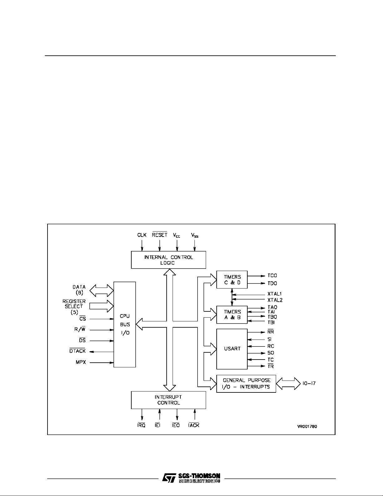
linesareprovided tofacilitate DMAC interfacing. Referto blockdiagram of the TS68HC901.
The TS68HC901 performs many of the functions
commonto most microprocessor-based systems.
The resources available to the userinclude:
.EightIndividually Programmable I/OPins withIn-
terrupt Capability
.16-Source Interrupt Controller with Individual
Source Enabling andMasking
.Four Timers, Two of which are Multi-Mode Ti-
mers
Figure 1: TS68HC901 Block Diagram
.Timers may be used as Baud Rate Generators
for the Serial Channel
.Single-Channel Full-Duplex Universal Synchro-
nous / Asynchronous Receiver-Transmitter (USART) thatSupports Asynchronous andwiththe
Addition of a Polynomial Generator Checker
Supports Byte Synchronous Formats
Byincorporating multiple functions withintheCMFP,
the systemdesigner retains flexibility while minimizing device count.
Froma programmer’s pointof view, theversatility of
the CMFPmay be attributed to its register set. The
registers arewell organized andallowthe CMFP to
be easily tailored to a varietyof applications. All of
the 24registers arealso directly addressable which
simplifies programming. The registermap is shown
in Figure2.
2/42

Address
Binary
Hex
RS5 RS4 RS3 RS2 RS1
TS68HC901
Figure 2 : CMFP Register Map.
Abbreviation Register Name
01
03
05
07
09
0B
0D
0F
11
13
15
17
19
1B
1D
1F
21
23
25
27
29
2B
2D
2F
Note : Hex addresses assume t hat R S1 connects wit h A 1, R S2connects with A2, et c... and t hat DS is connected to LDS on
the 68000 or D S i s connec t to DS on th e 68008.
0
1
0
0
0
0
0
1
0
0
0
1
1
0
0
0
0
0
1
0
0
1
0
1
0
0
0
1
1
0
0
1
1
1
0
0
0
0
0
1
0
1
0
0
1
0
0
1
0
1
0
1
1
0
1
0
0
0
1
1
0
1
0
1
1
0
0
1
1
1
0
1
1
1
1
0
0
0
0
0
1
1
0
0
0
1
0
1
0
0
1
1
1
0
0
1
0
0
1
0
1
1
0
1
0
1
0
1
1
0
1
1
1
1
0
1
0
0
0
0
GPIP
AER
DDR
IERA
IERB
IPRA
IPRB
ISRA
ISRB
IMRA
IMRB
VR
TACR
TBCR
TCDCR
TADR
TBDR
TCDR
TDDR
SCR
UCR
RSR
TSR
UDR
General Purpose I/O Register
Active Edge Register
Data DirectionRegister
Interrupt EnableRegister A
Interrupt EnableRegister B
Interrupt Pending Register A
Interrupt Pending Register B
Interrupt In-serviceRegister A
Interrupt In-serviceRegister B
Interrupt Mask Register A
Interrupt Mask Register B
Vector Register
Timer A Control Register
Timer B Control Register
Timers C and D Control Register
Timer A Data Register
Timer B Data Register
Timer C Data Register
Timer D Data Register
Synchronous Character Register
USART Control Register
Receiver Status Register
Transmitter StatusRegister
USART Data Register
3/42

TS68HC901
Figure 3 : PDIP Pin connection
Figure 4 : PLCC Pin connection
Pin MOTOROLA
6800 Type
MOTOROLA
Multiplexed
INTEL
PIN DESCR IPTIO N
GND : Ground
VCC: +5 volts(± 5%)
R/W : Read/Write (input). This input defines a
data transfert as a Read (High) or Write
(Low) cycle. This signal is used as WR
with an Intelprocessortype.
DTACK : This outputsignals the completion ofthe
operation phaseofa buscycleto theprocessor. If the bus cycle is a processor
read, the CMFP asserts DTACKto indicate thatthe information ontheData bus
is valid.If the buscycle is a processor to
the CMFP, DTACK acknowledges the
acceptance of the data by the CMFP.
DTACKwillbeassertedonlybyanCMFP
that has CS or IAK (and IEI) asserted.
This signal is not used with a 6800processortype.
48
47
35
CS
E
1
R/W
V
SS
CS
DS
R/W
AS
CS
RD
WR
ALE
CS : Chip Select (input, active low). CS is u-
sed to select theTS68HC901 CMFP for
accesses to the internal registers. CS
and IACK must not be asserted at the
same time.
DS : Data Stobe(input, active low).This Input
is part of the internal chip select and interrupt acknowledge functions.
The CMFP mustbe located on thelower
portionof the16-bit data-busso thatthe
vector number passed to the processor
during an interrupt acknowledge cycle
willbe located inthe low byte of the data
word.Asa result,DS mustbe connected
to the processor’s lower data strobe if
vectored interrupt are to be used. Note
thatthis forces all registers tobe located
atodd addresses and latchesdataonthe
risingedge forwrites.This signal isused
asRD with anIntel processor type.
4/42

TS68HC901
RS1-RS5:
(A1-A5)
Register Address Bus (inputs). The address bus is used to address one of the
internal registers during a read or write
cycle.
D0-D7: Data Bus (bi-directional, tri-stateable).
This bus is usedto receive data from or
transmit data totheMFP’sinternal registers duringa processor read orwrite cycle. During an interrupt acknowledge cycle, thedata busisused to pass a vector
numberto theprocessor. Since theMFP
is an 8-bit peripheral, the MFP could be
locatedon either theupper or lowerportion of the 16-bit data bus (even or odd
address). However, during an interrupt
acknowledge cycle, the vector number
passedto theprocessor must belocated
in thelow byteof thedata word.As aresult, D0-D7 of the MFPmustbe connected to the low eightbits of theprocessor
data bus, placing MFP registers at odd
addresses if vectored interrupt are to be
used.
CLK : The clock input is a single-phase TTL
compatible signal used for internal timing . This input shouldnot begated off
at any time and must conform to minimum and maximum pulse width times.
The clock is not necessarily the system
clock in frequency nor phase. When the
bus is multiplexed (MPX=1), an address
strobe signalis connected to this pin. In
the nonmultiplexed mode (MPX=0), this
input is connected to the system clock
when used with a 68000 processor type
or to VSS(0VDC) whenused witha 6800
processor type.
RESET : Device reset. (input, active low). Reset
disables the USARTreceiver and transmitter, stops alltimers and forces the timer outputs low, disables all interrupt
channels and clears any pending interrupts.The General Purpose Interrupt/I/O
lines will be placed in the tri-state input
mode.Allinternalregisters(exceptthetimer,USART dataregisters, and transmit
status register) willbe cleared.
MPX: This inputselects thedata bus mode:
MPX =0 : non multiplexed mode
MPX=1:multiplexed mode.Theregister
select lines RS1-RS5 and the data bus
D0 -D7 are mult iplexed. An ad dress
strobemustbeconnected totheCLKpin.
IRQ : Interrupt Request (output, active low, o-
pen drain). This output signals the processor that an interrupt is pending from
the CMFP.These are 16 interrupt channels that can generate an interrupt request. Clearing the interrupt pendingregisters (IPRA and IPRB) or clearing the
inte rr u pt mask regist ers (IMRA and
IMRB)willcauseIRQ to be negated. IRQ
willalso be negated astheresultof an interrupt acknowledge cycle, unless additional interrupts are pending in t he
CMFP. Ref er t o par agraph INTE RRUPTSfor further information.
IACK : Interrupt Acknowledge (input, act ive
low). IACK is used to signal the
TS68HC901 that the CPU is acknowledging an interrupt. CS and IACk must
not beasserted atthe same time.
IEI : Interrupt Enable In (input, active low). IEI
isusedtosignalthe TS68HC901 that no
higher priority device is requesting interrupt service.
IEO : InterruptEnable Out (output, activelow).
IEO is used to signal lower priority peripherals that neitherthe TS68HC901 nor
another higher priority peripheral is requesting interrupt service.
I0-I7 : General Purpose Interrupt I/O lines.
Theselines maybe usedas interrupt inputsand/orI/Olines.Whenusedasinterrupt inputs, their activeedge isprogrammable. Adatadirection register isusedto
define which lines are to be Hi-Z inputs
and which lines are to be push-pull TTL
compatible outputs.
SO : SerialOutput.This is theoutputof the U-
SART transmitter.
SI : Serial Input. This is the input to the U-
SART receiver.
RC : Receiver Clock. This input controls the
serialbit rate of the USARTreceiver.
TC : TransmitterClock.Thisinputcontrols the
serialbit rate of the USARTtransmitter.
RR : Receiver Ready. (output, active low)
DMA output for receiver, which reflects
the status of Buffer Full in port number
15.
TR : Transmitter Ready. (output, active low)
DMA output for transmitter, which reflects the status of Buffer Empty in port
number 16.
5/42

TS68HC901
TAO,TBO,
TCO,TDO:
Timer Outputs. Each of the four timers
has an output which can produce a
square wave. The output will change
states each timercycle; thusone fullperiod of thetimer out signal is equal to two
timer cycles. TAO or TBO can be reset
(logic ”O”)by a writeto TACR,or TBCR
respectively.
TAI,TBI: Timer A, B inputs. These inputs are
controlsignals for timers A and B in the
pulse width measurement mode and event count mode. These signals generate interrupts at the same priority level
asthegeneral purpose I/Ointerrupt lines
I4 and I3, respectively. I4 and I3 do not
haveinterrupt capability when thetimers
areoperated inthepulsewidthmeasure-
XTAL1,
XTAL2 :
Timer Clock inputs. A crystal can be
connectedbetween XTAL1 and XTAL2,
or XTAL1 can bedriven witha TTL level
clock.WhendrivingXTAL1with aTTLle-
mentmode orthe event countmode -under these conditions I4 and I3 may only
be used for I/O. Refer to paragraph TIMERSfor further information.
velclock,XTAL2 mustbeallowedtofloat.
Whenusingacrystal,external capacitors
are required. See figure 35. All chip acces s es are independent of t he tim er
clock.
SIGNAL SUMMARY.
Signal Name Mnemonic I/O Active
Power Input V
Ground GND Input Low
Clock CLK Input N/A
Chip Select CS Input Low
Data Strobe DS Input Low
Read/Write R/W Input Read-High / Write-Low
Data tranfer Acknowledge DTACK Output Low
Register Select Bus RS1-RS5 Input N/A
Data Bus D0-D7 I/O N/A
Reset RESET Input Low
Interrupt Request IRQ Output Low
Interrupt Acknowledge IACK Input Low
Interrupt Enable In IEI Input Low
Interrupt EnableOut IEO Output Low
General Purpose I/O - Interrupt Lines I0-I7 I/O N/A
Timer Clock XTAL1,XTAL2 Input High
Timer Inputs TAI, TBI Input N/A
Timer Outputs TAO, TBO, TCO, TDO Output N/A
Serial Input SI Input N/A
Serial Output SO Output N/A
Receiver Clock RC Input N/A
Transmitter Clock TC Input N/A
Receiver Ready RR Output Low
Transmitter Ready TR Output Low
MPX MPX Input N/A
CC
Input High
6/42

BUSOPERATION
Thefollowingparagraphs explain the controlsignals
and bus operation during data transfer operations
andreset.
DATA TRANSFER OPERATIONS.
Transfer ofdata between devicesinvolvesthe follo-
wing pins: Register Select Bus - RS5 throughRS1
DataBus - D0 throughD7 ControlSignals The address and databusesareseparate parallel busesused to transfer data using an asynchronous bus
structure.In all cycles, thebus master assumes responsibilityfordeskewing allsignals itissuesatboth
the start and end of a cycle. Additionally, the bus
master is responsible for deskewing the acknowledge and data signalsfrom theperipheral devices.
ReadCycle. To read a CMFP register, CS andDS
must be asserted, and R/W must be high. The
CMFPwill place the content of the registerwhich is
selected by the register select bus (RS1 through
RS5) on the data bus(D1 through D7)and then assertDTACK. The register addresses are shownon
Figure2. Aftertheprocessor has latchedthedata, DS
is negated. The negation of either CSor DS will terminate the read operation. The CMFP will drive
DTACKHigh andplace itinthehigh-impedance state.
Thetimingfor areadcycleis shown in figure 21.
WriteCycle.To writea register CSand DS must be
asserted,and R/W must below. TheCMFP willdecodetheaddress bus todetermine which registeris
selected. Then the register will be loaded with the
contentsof thedata bus and DTACK will be asserted. When the processor recognizes DTACK, DS
will be negated.The write cycle is terminated when
either CS or DS is negated. The CMFP will drive
DTACKhighandplaceitinthehigh-impedance state.
Thetimingfor awritecycleisshown in figure22.
TS68HC901
INTERRUPTACKNOWLEDGE OPERATION.
The CMFP has 16 interruptsources, eight internal
and eight external. When an interrupt request is
pending,theCMFPwillassertIRQ. In a vectored interruptscheme,the processor willacknowledge the
interruptrequestbyperforming aninterrupt acknowledge cycle. IACK and DS will be asserted. The
CMFPresponds totheIACKsignalbyplacing avector number on the lower eight bits of the data bus.
This vectornumber corresponds tothe IRQhandler
for the particular interrupt requesting service. The
format ofthis vector number is given in figure6.
Whenthe CMFPasserts DTACKtoindicate that valid data isonthebus, theprocessor willlatchthe data and terminate the bus cycle by negating DS.
WheneitherDS orIACKarenegated, theCMFPwill
terminate the interrupt acknowledge operation by
driving DTACK high and placingit inthe high-impedance state. Also, thedata buswillbe placed in the
high-impedance state.IRQ will benegatedas a result of the IACK cycle unless additional interrupts
are pending.
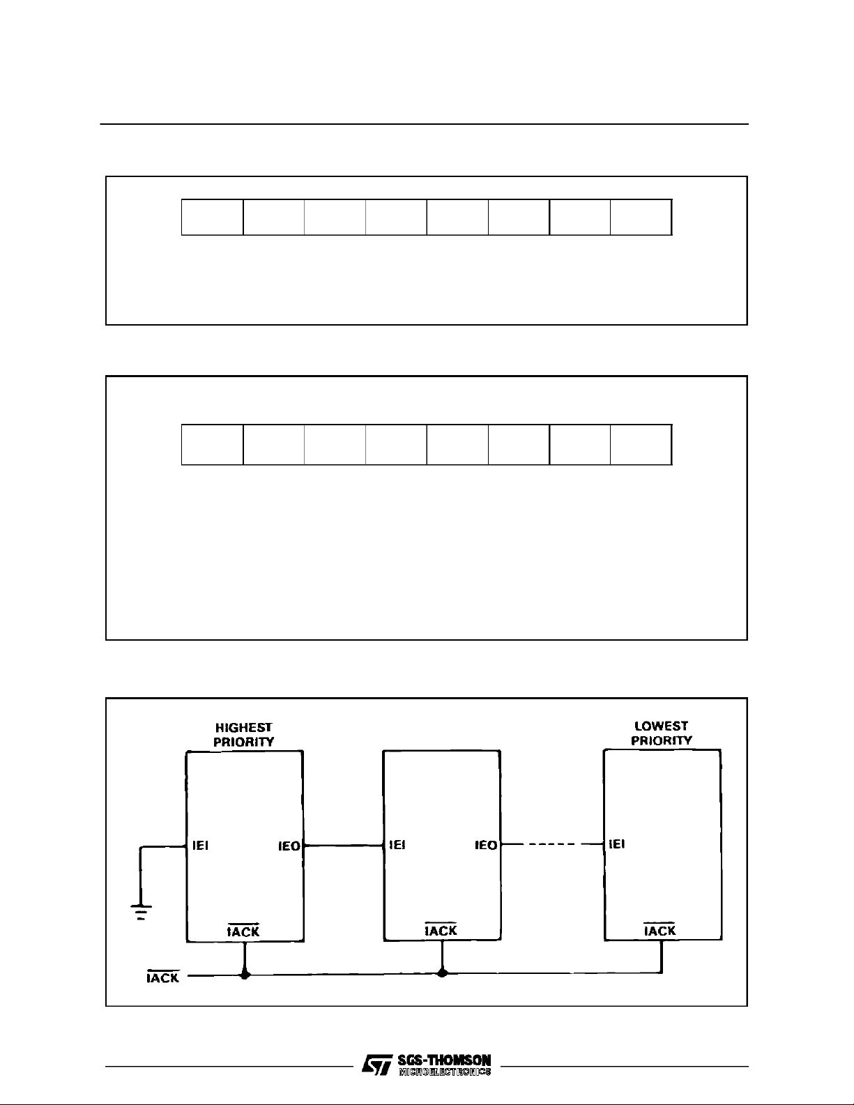
The CMFP can be part of a daisy-chain interrupt
structurewhich allows multiple CMFPsto be placed
at the same interrupt level by sharing a common
IACK signal.A daisy-chain priority schemeisimplemented with IEI and IEO signals. IEI indicates that
no higherpriority device is requesting interrupt service. IEOsignals lowerpriority devices that neither
this devicenor any higher priority devices is requesting service. To daisy-chain CMFPs, the highest
priority CMFP has its IEI tied low and successive
CMFPs havetheirIEI connected to the next higher
priority device’sIEO.Notethatwhenthedaisy-chain
7/42

TS68HC901
interrupt structure is notimplemented, the IEI of all
CMFPsmust betied low.
When the processor initiates an interrupt acknowledge cycle by driving IACK and DS, the CMFP
whoseIEI is low may respond witha vectornumber
if interrupt is pending. If this device doesnot have a
pending interrupt, IEO is asserted which allowsthe
nextlowerpriority device to respond to the interrupt
acknowledge. When an CMFP propagates IEO, it
willnot drive thedata bus norDTACK during the interruptacknowledge cycle. The timingfor an IACK
cycleis shown in figure 23 and 24.
RESET OPERATION
The reset operation will initialize the CMFP to a
known state. Thereset operation requires that the
RESET input be asserted for a minimum of two
microseconds. During a device reset condition, all
internal CMFP registers are cleared except for the
timer data registers (TADR, TBDR, TCDR and
TDDR), the USART data register (UDR), the transmitterstatus register (TSR) andthe interrupt vector
register. Alltimers are stopped and the USART receiver and transmitter are disabled. The interrupt
channelsare also disabled and any pending inter-
rupts are cleared. In addition, the general purpose
interruptI/Olinesare placed in thehigh-impedance
inputmode andthetimeroutputsaredrivenlow. ExternalCMFPsignalsarenegated.The interrupt vector register is initialized to a0Fh.
NON MULTIPLEXED MODE
In this mode, theMPX inputmustbe setto zero, and
the TS68HC901 can be used witha 68000 processortype or a6800processor type.Referto figure 21
to 24for the electrical characteristics.
With a6800processor typetheDS pin isconnected
to the E signal of the processor, the DTACK signal
is not usedand the CLKmust be zeroed.
MULTIPLEXED MODE
The CMFPcan beusedeitheron aMOTOROLAor
INTELbus type. Inthiscasethe MPX pinisconnected to Vcc. The table page4 givesthe signification
ofthe differentsignals used. Adummyaccessto the
TS68HC901 hasto be done beforeany validaccess
in orderto set upthe internal logicof sampling.
8/42

TS68HC901
INTERRUPT STRUCTURE
In a 68000 system, the CMFP will be assigned to
oneof the sevenpossible interrupt levels.All interrupt service requests from the CMFP’s 16 interrupt
channelswillbepresented atthislevel.Although,as
an interrupt controller, the CMFP will internally prioritize its 16 interrupt sources. Additional interrupt
sourcesmay be placed at the same interrupt level
bydaisy-chaining multipleCMFPs.The CMFPswill
be prioritized bytheir position in the chain.
INTERRUPTPROCESSING
Each CMFP provides individual interrupt capability
for itsvarious functions. When aninterrupt isreceivedononeofthe external interrupt channels or from
oneof theeight internal sources,the CMFP willrequest interrupt service. The 16 interrupt channels
areassigneda fixedpriorityso thatmultiplepending
interrupts areservicedaccordingto theirrelativeimportance. Since the CMFP can internally generate
16vectornumbers, the unique vectornumber which
corresponds to the highest priority channel that as
apending interrupt ispresented totheprocessorduring an interrupt acknowledge cycle. This unique
vectornumber allows theprocessor to immediately
beginexecution of theinterrupt handler fortheinterrupt source,decreasing interrupt latencytime.
INTERRUPTCHANNEL PRIORITIZATION
The 16 interrupt channels are prioritized as shown
in figure5. General purpose interrupt 7(I7)is thehighest priority interrupt channel and I0 is the lowest
priority channel.Pendinginterruptsarepresented to
the CPU in order of priority unless theyhave been
masked off. By selectively masking interrupts, the
channelare in effectre-prioritized.
INTERRUPTVECTORNUMBER FORMAT
During an interrupt acknowledge cycle,a unique 8-
bit vector number is presented to the systemwhich
corresponds tothespecificinterrupt source which is
requesting service. The format of the vector is
shown in figure 6. The most significant four bits of
the interruptvectornumberareuserprogrammable.
These bits are set by writing the upper four bits of
the vector register which is shown in figure 7. The
low order bits are generated internally by the
TS68HC901. Note that the binary channel number
shown in figure 5 corresponds to the low order bits
of thevector number associated witheach channel.
Figure 9 : Interrupt Channel Prioritization
Figure 5 : Interrupt Channel Prioritization
Priority Channel Descriptio n
HIGHEST
LOWEST
1111
1110
1101
1100
1011
1010
1001
1000
0111
0110
0101
0100
0011
0010
0001
0000
General Purpose Interrupt 7(I7)
General Purpose Interrupt 6(I6)
Timer A
Receive Buffer Full
Receive Error
Transmit Buffer Empty
Transmit Error
Timer B
General Purpose Interrupt 5(I5)
General Purpose Interrupt 4(I4)
Timer C
Timer D
General Purpose Interrupt 3(I3)
General Purpose Interrupt 2(I2)
General Purpose Interrupt 1(I1)
General Purpose Interrupt 0(I0)
9/42
TS68HC901
V7 V6 V5 V4 IV3 IV2 IV1 IV0
V7-V4 The four mostsignificant bitsare copied from the register
IV3-IV0 These bitsare supplied by the CMFP.They are thebinary channel number of the highest
priority channel that is requesting interrupt service.
Figure 6 :
Figure 7 :
VR
(17h)
7
V7 V6 V5 V4 S 0* 0* 0*
Writin g 0 : CLEARED
Writing 1 : SET
CLEARED on RESET
VECTOR REGISTER
0
V7-V4 The upper fourbitsof the vectorregister are writtenby the user. These bits become themost
significant four bits of the interrupt vector number.
S In-Service Register Enable. When the Sbit is zero,the CMFP isin the automatic end-of-in-
terrupt mode and the In-Service register bits are forced low. When the S bit is a one, the
CMFP isin the software end-of-interrupt mode and the In-Service register bits areenabled.
* Unused bits,read as zero.
Figure 8 : Daisy Chaining
TS68HC901 TS68HC901
TS68HC901
10/42

TS68HC901
DAISY-CHAINING CMFPs
As an interrupt controller, the TS68HC901 CMFP
willsupport eight external interrupt sources in addition to its eight internal interrupt sources. When a
system requires more than eight external interrupt
sources to be placed at the same interrupt level,
sourcesmaybe added totheprioritized structureby
daisy-chaining CMFPs. Interrupt sources areprioritized internally within each CMFP and the CMFPs
areprioritized by their position inthe chain. Unique
vector numbers are provided for each interrupt
sources.
The IEI and IEO signals implement the daisy-chainedinterrupt structure.TheIEIofthehighest priority
CMFPis tied low and the IEO output of this device
is tied to the next highest priority CMFP’s IEI. The
IEI andIEO signalsaredaisy-chainedinthismanner
for all CMFPs in the chain, with the lowest priority
CMFP’s IEO left unconnected. A diagram of an interrupt daisy-chain is shownin figure8.
Daisy-chaining requires that all parts in the chain
have a commonIACK. Whenthe common IACK is
asserted duringan interrupt acknowledge cycle, all
partswillprioritize interrupts inparallel.Whenthe IEI
signalto aCMFP is asserted, the part may respond
to the IACK cycle if it requires interrupt service.
Otherwise,the partwill assert IEO tothe next lower
priority device. Thus, priority is passed down the
chainvia IEI andIEO until a part whichhas appending interrupt isreached. Thepart with the pending
interrupt passes a vector number to the processor
and doesnot propagate IEO.
Figure 9a :
Figure 9b :
11/42

TS68HC901
INTERRUPTCONTROL REGISTERS
CMPFinterruptprocessing ismanagedbytheinter-
rupt enable registers A andB, interrupt pending registersA andB, andinterrupt mask registers A and
B.These registers allow theprogrammer to enable
or disable individual interrupt channels, mask individual interrupt channels,and accesspending interruptstatusinformation. In-service registers Aand B
allow interrupts tobe nestedas describedhereafter.
The interrupt control registers are shown in figure10.
INTERRUPTENABLE REGISTERS
Theinterrupt channels are individually enabled ordi-
sabledby writing a one or zero,respectively, tothe
appropriate bit of interrupt enable register A(IERA)
or interrupt enable register B (IERB).Theprocessor
may readthese registers at anytime.
When a channel is enabled, interrupts received on
the channel will be recognized by the CMFP and
IRQwillbe asserted tothe processor,indicatingthat
interrupt service isrequired. On the otherhand, adisabledchannel is completely inactive; interrupts receivedon the channel are ignored by theCMFP.
Writinga zero to a bitof interrupt enable register A
orB willcausethecorresponding bitofinterrupt pendingregister A orB tobe cleared. This willterminate
allinterrupt service requests forthe channel and also negate IRQ,unless interrupts are pending from
other sources. Disabling a channel, however,does
not affect the corresponding bit in interrupt in-serviceregistersA or B. So, if theCMFPis in thesoftware end-of-interrupt mode and an interrupt is in
service whena channel will remainset until cleared
bysoftware.
INTERRUPTPENDINGREGISTERS
When aninterrupt is received onan enabled chan-
nel, the corresponding interrupt pending bitis set in
interrupt pending register A orB (IPRAor IPRB). In
a vectoredinterruptscheme, thisbit willbe cleared
when the processor acknowledges the interrupting
channeland the CMFPresponds witha vectornumber. In a polled interrupt system, the interrupt pending registers must be read to determine the interruptingchannel andthentheinterrupting pending bit
is cleared by the interrupt handling routine without
performing aninterrupt acknowledge sequence.
A singlebit of theinterrupt pending registers iscleared insoftwareby writing onesto all bitpositionsexcept thebit to be cleared. Note that writing ones to
IPRA and IPRB has no effect on the contents of the
register. A single bit of the interrupt pending registersisalsoclearedwhenthecorresponding channel
is disabled bywriting azero tothe appropriate bitof
IERA orIERB.
INTERRUPTMASK REGISTERS
Interrupts are masked for a channel by clearing the
appropriate bitin interrupt mask register Aor B(IMRA or IMRB). Even though an enabled channel is
masked, the channel will recognize subsequent interruptsand set its interrupt pending bit. However,
the channel is prevented from requesting interrupt
service(IRQ tothe processor) as long as the mask
bit forthat channel is cleared.
If achannelisrequestinginterruptserviceatthetime
that its corresponding bit in IMRA or IMRBis cleared, the request will ceaseandIRQ will benegated,
unless anotherchannel is requesting interrupt service.Later,whenthemaskbit isset,any pendinginterrupt on thechannel will be processed according
to the channel’s assigned priority. IMRAand IMRB
may be read at any time.
12/42
TS68HC901
Figure 10 :
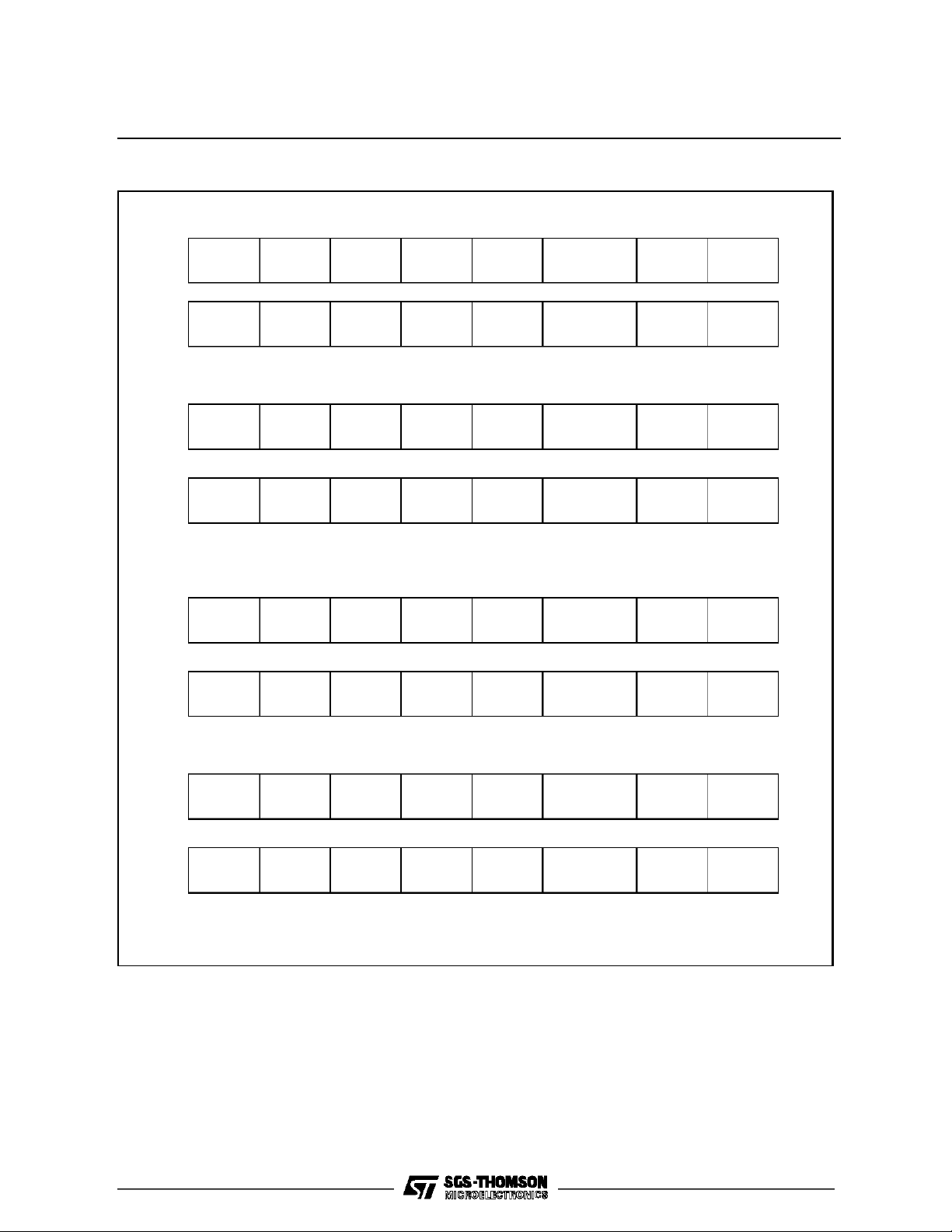
IERA
(07h)
IERB
(09h)
IPRA
(0Bh)
IPRB
(0Dh)
ISRA
(0Fh)
7
GPIP7 GPIP6 TIMER A
GPIP5 GPIP4 TIMER C TIMER D GPIP3 GPIP2 GPIP1 GPIP0
7
GPIP7 GPIP6 TIMER A
GPIP5 GPIP4 TIMER C TIMER D GPIP3 GPIP2 GPIP1 GPIP0
Writing0:CLEAR
Wri ting 1 : UNCHANG ED
7
GPIP7 GPIP6 TIMER A
INTERRUPT ENABLEREGISTERS
RCV
Buffer full
RCV
Error
XMIT
Buffer Empty
INTERRUPT PENDING REGISTERS
RCV
Buffer full
RCV
Error
XMIT
Buffer Empty
INTERRUPT IN-SERVICEREGISTERS
RCV
Buffer full
RCV
Error
XMIT
Buffer Empty
XMIT
Error
XMIT
Error
XMIT
Error
0
TIMER B
0
TIMER B
0
TIMER B
ISRB
(11h)
IMRA
(13h)
IMRB
(15h)
GPIP5 GPIP4 TIMER C TIMER D GPIP3 GPIP2 GPIP1 GPIP0
7
GPIP7 GPIP6 TIMER A
GPIP5 GPIP4 TIMER C TIMER D GPIP3 GPIP2 GPIP1 GPIP0
Writing 0 : MASKED
Writing 1 : UN MASKED
INTERRUPT MASK REGISTERS
RCV
Buffer full
RCV
Error
Buffer Empty
XMIT
XMIT
Error
0
TIMER B
13/42
 Loading...