

TS4851
MONO 1 W SPEAKER AND STEREO 160 mW HEADSET
BTL DRIVERS WITH DIGITAL VOLUME CONTROL
■ Operating from VCC=3V to 5.5V
■ Rail to rail input/output
■ Speaker driver with 1 W output @
Vcc=5V, THD+N=1%, F=1kHz, 8Ω load
■ Headset drivers with 160 mW output @
Vcc = 5 V, THD+N = 1%, F = 1 kHz, 32 Ω load
■ Headset output is 30 m W i n stereo @
Vcc=3V
■ THD+N < 0.5% Max @ 20 mW into 32
Ω
BTL, 50 Hz < Frequency < 20 kHz
■ 32-step di gi t al vol um e control from -
34.5 dB to +12 dB
■ +6 dB power up volume and full standby
■ 8 diffe rent output mod es
■ Pop & click reduction circuitry
■ Low shutdown current (< 100 nA)
■ Thermal shutdown pr otection
■ Flip-chip package 18 x 300 µm bumps
DESCRIPTION
The TS4851 is a low power audio amplifier that
can drive either b oth a mon o speake r or a ste reo
headset. To the speaker, it can deliver 400 mW
(typ.) of continuous RMS output power into an 8
load with a 1% THD+N value. To the headset
driver, the amplifier can deliver 30 m W (typ.) per
channel of continuous average power into a
stereo 32
@ 3.3 V.
Ω bridged-tied load with 0.5% THD+N
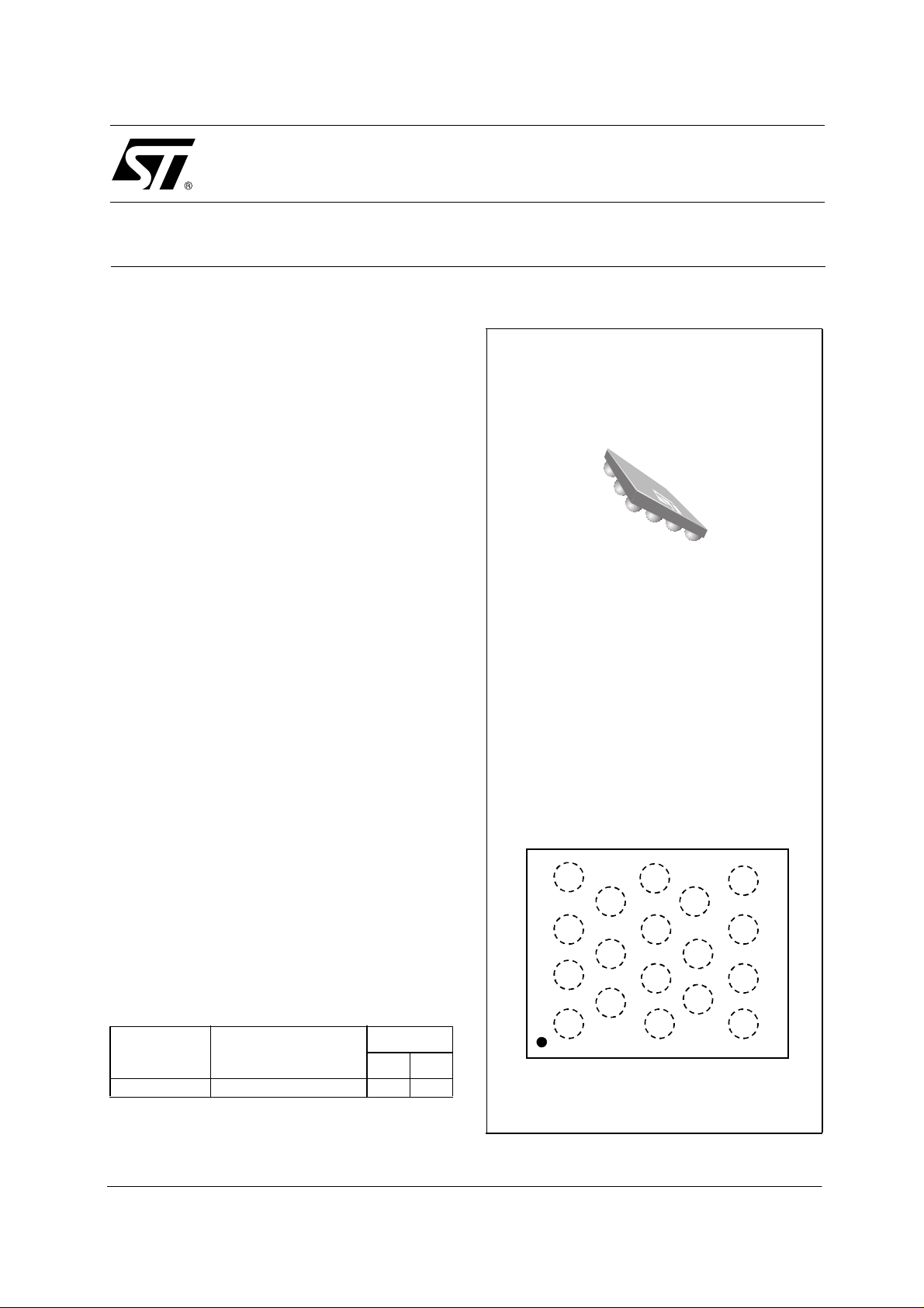
PIN CONNECTIONS (top view)
TS485IJT - Flip Chip
Ω
Pin Out (top view)
This device features a 32-step digital volume
control and 8 different output selections. The
digital volume and output modes are controlled
through a three-digit SPI interface bus.
APPLICATIONS
■ Mobile Phones
ORDER CODE
R
R
OUT<
OUT<
-
-
R
R
IN
IN
PHONE
PHONE
IN
IN
BYPASS
BYPASS
OUT +
OUT +
IN
IN
SPKR
SPKR
OUT+
OUT+
GND
GND
R
R
VCC DATA
VCC DATA
L
L
VCC
VCC
GND CLK
GND CLK
L
L
OUT +
OUT +
SPKR
SPKR
OUT -
OUT -
L
L
OUT -
OUT -
NC
NC
ENB
ENB
Package
Part Number Temperature Range
J
TS4851IJT -40, +85°C
J = Flip Chip Package - only available in Tape & Reel (JT))
•
April 2003 Revision B 1/26
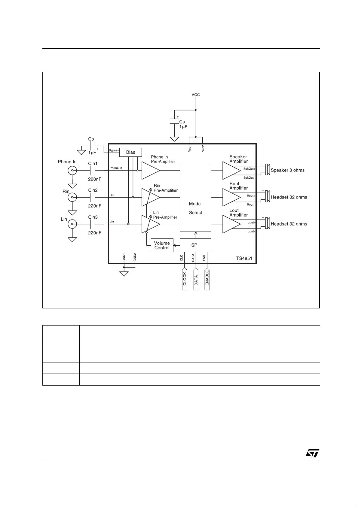
TS4851 Application Information for a Typical A pp lication
1 APPLICATION INFORMATION FOR A TYPICAL APPLICATION
External component descriptions
Component Functional Description
This is the input coupling capacitor. It blocks the DC voltage at, and couples the input signal to the
amplifier’s input terminals. Cin also creates a highpass filter with the internal input impedance Zin at Fc
=1/ (2
πi x Zin x Cin).
This is the Supply Bypass capacitor. It provides power supply filtering.
This is the Bypass pin capacitor. It provides half-supply filtering.
2/26
C
in
C
s
C
B
SPI Bus Interface TS4851
2 SPI BUS INTER FACE
2.1 Pin descriptions
Pin Functional Description
DATA This is the serial data input pin.
CLK This is the clock input pin.
ENB This is the SPI enable pin active at high level.
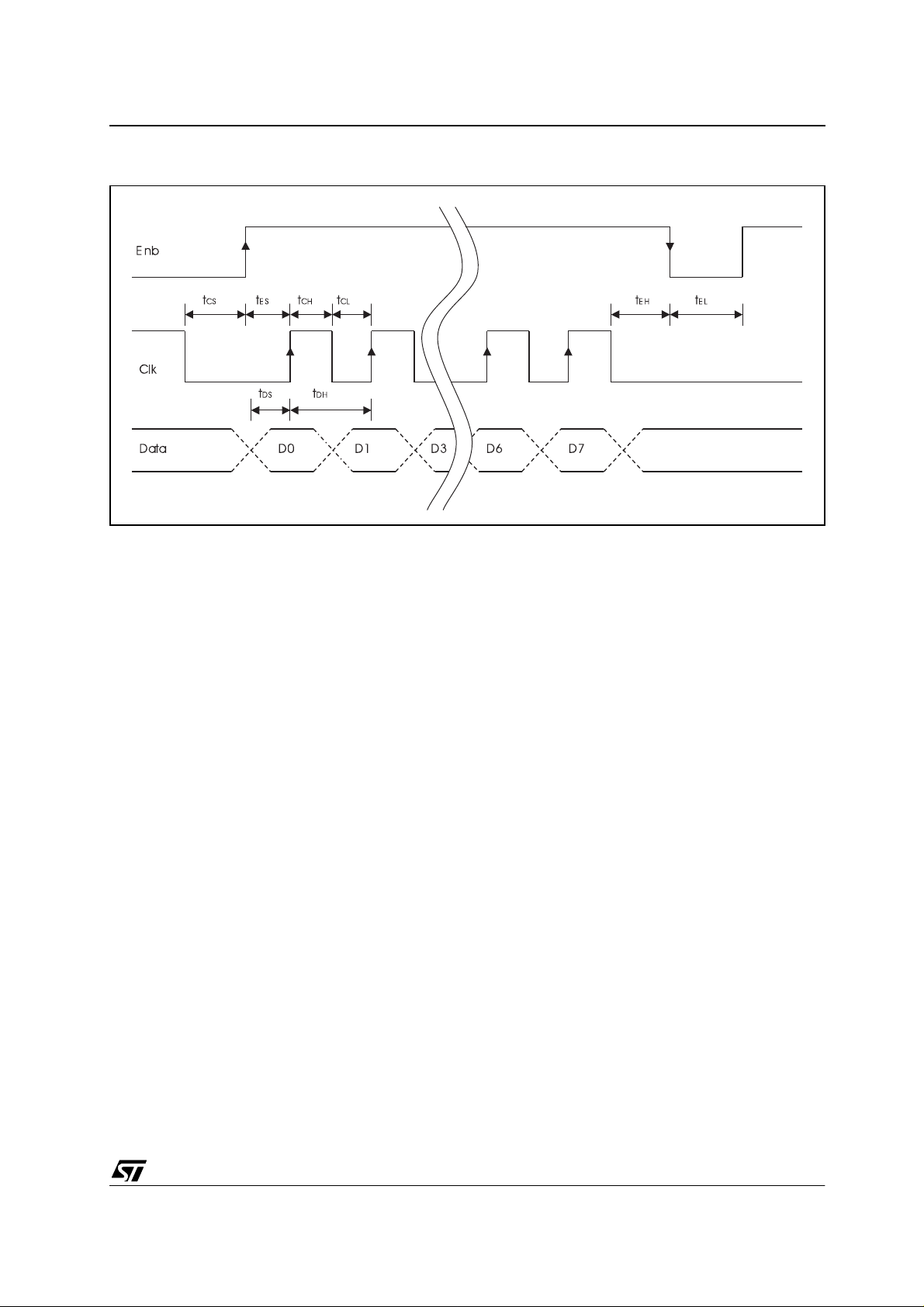
2.2 Description of SPI operation
The serial data bits are organized into a field
containing 8 bits of data as shown in
Table 1
. The
first 8 bits will get loaded into the shift register and
the rest of the bits will be disregarded.
Ta ble 1: Bit Allocatio n
DATA 0 to DATA 2 bits determine the output
mode of the TS4851 as shown in
Table 2
. The
DATA 3 to DATA 7 bits determine the gain level
setting as illustrated by
Table 3
. For each SPI
transfer, the data bits are written to the DATA pin
with the least significant bit (LSB) first. All serial
data are sampled at the rising edge of the CLK
signal. Once all the dat a bi ts h ave been sampled,
ENB transitions from logic-high to logic low to
complete the SPI sequence. All 8 bits must be
LSB DATA 0 Mode 1
DA TA MODES
DATA 1 Mode 2
DATA 2 Mode 3
DATA 3 gain 1
DATA 4 gain 2
DATA 5 gain 3
received before any data latch can occur. Any
excess CLK and DATA tran sitio ns w ill b e igno red
after the height rising clock edge has occurred.
MSB DATA 7 gain 5
DATA 6 gain 4
For any data sequence longer than 8 bits, only the
Table 2: Outpu t mode selection: G from -34.5 dB to +12 dB (by steps of 1.5 dB)
Output
Mode #
0 0 0 0 SD SD SD
1 0 0 1 6dBxP SD SD
2 0 1 0 SD 0dBxP 0dBxP
3 0 1 1 Gx(R+L) SD SD
4 1 0 0 SD GxR GxL
5 1 0 1 Gx(R+L)
6 1 1 0 SD GxR+0dBxP GxL+0dBxP
7 1 1 1 6dBxP GxR+0dBxP GxL+0dBxP
DATA 2 DATA 1 DATA 0
SPKERout
+6dBxP
1
Rout Lout
SD SD
1) SD = Shutd own Mode, P = Phone in Input, R = Rin input and L = Li n i nput
3/26
TS4851 SPI Bus Interface
Table 3: Volume Control Settings
K :
Gain (dB) DATA 7 DATA 6 DATA 5 DATA 4 DATA 3
-34.5 0 0 0 0 0
-33.0 0 0 0 0 1
-31.5 0 0 0 1 0
-30.0 0 0 0 1 1
-28.5 0 0 1 0 0
-27.0 0 0 1 0 1
-25.5 0 0 1 1 0
-24.0 0 0 1 1 1
-22.5 0 1 0 0 0
-21.0 0 1 0 0 1
-19.5 0 1 0 1 0
-18.0 0 1 0 1 1
-16.5 0 1 1 0 0
-15.0 0 1 1 0 1
-13.5 0 1 1 1 0
-12.0 0 1 1 1 1
-10.5 1 0 0 0 0
-9.0 1 0 0 0 1
-7.5 1 0 0 1 0
-6.0 1 0 0 1 1
-4.5 1 0 1 0 0
-3.0 1 0 1 0 1
-1.5 1 0 1 1 0
0.0 10111
1.5 11000
3.0 11001
4.5 11010
6 11011
7.5 11100
9 11101
10.5 1 1 1 1 0
12 11111
4/26
SPI Bus Interface TS4851
2.3 SPI Timing Diagram
5/26
TS4851 Absolute Maximum Ratings
3 ABSOLUTE MAXIMUM RATINGS
Symbol Parameter Value Un it
VCC
T
oper
T
stg
T
R
thja
Supply voltage
Operating Free Air Temperature Range -40 to + 85 °C
Storage Temperature -65 to +150 °C
Maximum Junction Temperature 150 °C
j
Flip Chip Thermal Resistance Junction to Ambient
Pd Power Dissipation Internally Limited
ESD Human Body Model 2 kV
ESD Machine Model 100 V
Latch-up Immunity 200 mA
Lead Te mpera ture (solde ring, 10se c) 250 °C
1) All volta ges values are me asured with r espect to the ground pin.
2) D evice is prote ct ed in case of over temperature by a thermal shutdown act i ve @ 150°C
1
2
6V
200 °C/W
4 OPERATING CONDITIONS
Symbol Parameter Value Unit
VCC Supply Voltage 3 to 5.5 V
V
phin
Maximum Phone In Input Voltage GND to VCC V
VRin/VLin Maximum Rin & Lin Input Voltage G
TSD Thermal Shut Down Temperature 150 °C
R
thja
1) D evice is prote ct ed in case of over temperature by a thermal shutdown act i ve @ 150°C
Flip Chip Thermal Resistance Junction to Ambient
1
to V
ND
CC
90 °C/W
V
6/26
Electrical Characteristics TS4851
5 ELECTRICAL CHARACTERISTICS
Table 4: Electrical characteristics at VCC = +5 V, GND = 0 V, Tamb = 25°C (unless otherwise
specified)
Symbol Parameter Min. Typ. Max. Unit
I
CC
I
STANDBY
Supply Current
Output Mode 7, Vin = 0 V, no load
All other output modes, Vin = 0 V, no load
Standby Current
8
4.5
11
mA
6.5
µA
Output Mode 0 0.1 2
Voo Output Offset Voltage (differential)
mV
Vin = 0 V 5 50
Vil “Logic low” input Voltage 0 0.4 V
Vih “Logic high” input Voltage 1.4 5 V
Po Output Power
SPKERout, RL = 8
Rout & Lout, RL = 32
THD = 1%, F = 1 kHz
Ω,
THD = 0 .5%, F = 1 kHz
Ω,
THD + N Total Harmonic Distortion + Noise
Rout & Lout, Po = 80 mW, F = 1 kHz, RL = 32
SPKERout, Po = 800 mW, F = 1 kHz, RL = 8
Rout & Lout, Po = 50 mW, 20 Hz < F < 20 kHz, RL = 32
SPKERout, Po = 40 mW, 20 Hz < F < 20 kHz, RL = 8
800801000
120
Ω
Ω
Ω
Ω
0.5
1
0.5
1
mW
%
SNR Signal To Noise Ratio (A-Weighted) 90 dB
1
PSRR
Power Supply Rejection Ratio (Output Mode = 2)
Vripple = 200 mV Vpp, F = 217 Hz, Input Floating
Vripple = 200 mV Vpp, F = 217 Hz, Input Terminated 10
G Digital Gain Range - Rin & Lin
2
dB
61
Ω
62
dB
no load -34.5 +12
Digital gain stepsize 1.5 dB
Stepsize
G ≥ -22.5 dB
G < -22.5 dB
-0.5
-1
+0.5
+1
Phone In Gain, no load
BTL gain from Phone In to SPKERout
BTL gain from Phone In to Rout & Lout
6
0
Zin Phone In Input Impedance 15 20 25 k
Zin Rin & Lin Input Impedance (all gain setting) 37.5 50 62.5 k
dB
dB
Ω
Ω
tes Enable Stepup Time - ENB 20 ns
teh Enable Hold Time - ENB 20 ns
tel Enable Low Time - ENB 30 ns
tds Data Setup Time- DATA 20 ns
tdh Data Hold Time - DATA 20 ns
tcs Clock Setup time - CLK 20 ns
tch Clock Logic High Time - CLK 50 ns
tcl Clock Logic Low Time - CLK 50 ns
fclk Clock Frequency - CLK DC 10 MHz
1) All PSRR data limits are guaranted by evaluation desgin test.
2) Dynamic measurements [20 x log(rms(Vout)/rms (Vripple)] . V ri pple is the sup eri m posed sinus si gnal to Vcc @ F = 217 Hz
7/26
TS4851 Electrical Characteristics
Table 5: El ectri cal character istics at VCC = +3.0V, GND = 0V, Tamb = 25°C (unless otherwise
specified)
Symbol Parameter Min. Ty p. Max. Unit
I
CC
I
STANDBY
Voo Output Offset Voltage (differential)
Supply Current
Output Mode 7, Vin = 0 V,no load
All other output modes, Vin = 0 V,no load
7.5
4.5
6.5
Standby Current
Output Mode 0 0.1 2
mA
10
µA
mV
Vin = 0 V 5 50
Vil “Logic low” input Voltage 0 0.4 V
Vih “Logic high” input Voltage 1.4 5 V
Po Output Power
SPKERout, RL = 8
Rout & Lout, RL = 32
THD = 1%, F = 1 kHz
Ω,
THD = 0.5%, F = 1 kHz
Ω,
THD + N Total Harmonic Distortion + Noise
Rout & Lout, Po = 20 mW, F = 1 kHz, RL = 32
SPKERout, Po = 300 mW, F = 1 kHz, RL = 8
Rout & Lout, Po = 15 mW, 20 Hz < F < 20 kHz, RL = 32
SPKERout, Po = 250 mW, 20 Hz < F < 20 kHz, RL = 8
300
20
Ω
Ω
Ω
Ω
340
30
0.5
1
0.5
1
mW
%
SNR Signal To Noise Ratio (A-Weighted) 86 dB
1
PSRR
Power Supply Rejection Ratio (Output Mode = 2)
Vripple = 200 mV Vpp, F = 217 Hz, Input Floating
Vripple = 200 mV Vpp, F = 217 Hz, Input Terminated 10
G Digital Gain Range - Rin & Lin
2
dB
61
Ω
62
dB
no load -34.5 - +12
Digital gain stepsize 1.5 dB
Zin
Zin
Stepsize error
G ≥ -22.5 dB
G < -22.5 dB
Phone In Gain, no load
BTL gain from Phone In to SPKERout
BTL gain from Phone In to Rout & Lout
Phone In Input Impedance
1
Rin & Lin Input Impedance (All Gain Setting)
-0.5
-1
+0.5
+1
6
0
15 20 25 k
1
37.5 50 62.5 k
dB
dB
tes Enable Stepup Time - ENB 20 ns
teh Enable Hold Time - ENB 20 ns
tel Enable Low Time - ENB 30 ns
tds Data Setup Time- DATA 20 ns
tdh Data Hold Time - DATA 20 ns
tcs Clock Setup time - CLK 20 ns
tch Clock Logic High Time - CLK 50 ns
tcl Clock Logic Low Time - CLK 50 ns
fclk Clock Frequency - CLK DC 10 MHz
Ω
Ω
1) All PSRR data limits are guaranted by evaluation desgin test.
2) Dynamic measurements [20 x log(rms(Vout)/rms (Vripple)] . V ri pple is the sup eri m posed sinus si gnal to Vcc @ F = 217 Hz.
8/26

Electrical Characteristics TS4851
Index of Graphics
Description Figure Page
THD + N vs. Output Power
THD + N vs. Frequency
Output Power vs. Power Supply Voltage
PSRR vs. Frequency
Frequency Response
Signal to Noise Ratio vs. Power Supply Voltage
Crosstalk vs. Frequency
-3 dB Lower Cut Off Frequency vs. Input Capacitor
Current Consumption vs. Power Supply Voltage
Power Dissipation vs. Output Power
Power Derating Curves
-3 dB Lower Cut Off Frequency vs. Gain Setting
Figures 1
Figures 11
Figures 21
Figures 29
Figures 39
Figures 43
Figures 47
Figures 49
to
10 page 10
to
20 page 11
to
28 page 13
to
38 page 14
to
42 page 16
to
46 page 17
to
48 page 18
to
50 page 18
Figure 51 page 18
Figures 52
to
55 page 18
Figure 56 page 19
Figure 57 page 19
to
to
to
to
to
page 11
page 13
page 14
page 16
page 19
Note: In the graph s tha t fol low, the a bbreviations Spkout = Speaker Output, and HDout = Headphone Output are
used.
All measurements made with Cin = 220 nF, Cb = Cs = 1 µF except in PSRR condition where Cs = 0.
9/26

TS4851 Electrical Characteristics
1E-3 0.01 0.1 1
0.1
1
10
Vcc=3V
F=20kHz
Vcc=5V
F=20kHz
Vcc=3V
F=1kHz
Vcc=5V
F=1kHz
RL = 4
Ω
Out. Mode = 3
G = +12dB
BW < 125kHz
Tamb = 25°C
THD + N (%)
Output Power (W)
Figure 1: S pko ut TH D+N vs. output po we r
(output modes 1, 7)
10
RL = 4
Ω
Out. Mode = 1, 7
BW < 125kHz
Tamb = 25°C
1
THD + N (%)
0.1
1E-3 0.01 0.1 1
Vcc=3V
F=20kHz
Vcc=5V
F=20kHz
Vcc=3V
F=1kHz
Output Power (W)
Vcc=5V
F=1kHz
Figure 2: S pko ut TH D+N vs. output po we r
(output modes 1, 7)
10
RL = 8
Ω
Out. Mode = 1, 7
BW < 125kHz
Tamb = 25°C
1
THD + N (%)
0.1
1E-3 0.01 0.1 1
Vcc=3V
F=20kHz
Vcc=3V
F=1kHz
Vcc=5V
F=20kHz
Vcc=5V
F=1kHz
Output Power (W)
Figure 4: HDout THD+N vs. outpu t power
(output mo de 2 )
10
RL = 16
Ω
Out. Mode = 2
BW < 125kHz
Tamb = 25°C
1
THD + N (%)
0.1
0.01
1E-3 0.01 0.1
Vcc=5V
F=20kHz
Vcc=3V
F=20kHz
Vcc=3V
F=1kHz
Output Power (W)
Vcc=5V
F=1kHz
Figure 5: HDout THD+N vs. outpu t power
(output mo de 2 )
10
RL = 32
Ω
Out. Mode = 2
BW < 125kHz
Tamb = 25°C
1
THD + N (%)
0.1
0.01
1E-3 0.01 0.1
Vcc=5V
F=20kHz
Vcc=3V
F=20kHz
Vcc=3V
F=1kHz
Output Power (W)
Vcc=5V
F=1kHz
Figure 3: S pko ut TH D+N vs. output po we r
(output modes 1, 7)
10
RL = 16
Ω
Out. Mode = 1, 7
BW < 125kHz
Tamb = 25°C
1
THD + N (%)
0.1
10/26
0.01
1E-3 0.01 0.1 1
Vcc=5V
F=20kHz
Vcc=3V
F=20kHz
Vcc=3V
F=1kHz
Output Power (W)
Figure 6: S pko ut TH D+N vs. output po we r
(output mode 3, G=+1 2 dB )
Vcc=5V
F=1kHz

Electrical Characteristics TS4851
1E-3 0.01 0.1
0.1
1
10
Vcc=3V
F=20kHz
Vcc=5V
F=20kHz
Vcc=3V
F=1kHz
Vcc=5V
F=1kHz
RL = 32
Ω
Out. Mode = 4
G = +12dB
BW < 125kHz
Tamb = 25°C
THD + N (%)
Output Power (W)
Figure 7: S pko ut TH D+N vs. output po we r
(output mode 3, G=+12dB)
10
RL = 8
Ω
Out. Mode = 3
G = +12dB
BW < 125kHz
Tamb = 25°C
1
THD + N (%)
0.1
Vcc=3V
F=1kHz
1E-3 0.01 0.1 1
Vcc=3V
F=20kHz
Output Power (W)
Vcc=5V
F=20kHz
Vcc=5V
F=1kHz
Figure 8: S pko ut TH D+N vs. output po we r
(output mode 3, G=+1 2 dB )
10
RL = 16
Out. Mode = 3
G = +12dB
BW < 125kHz
Tamb = 25°C
1
Ω
Vcc=3V
F=20kHz
Vcc=5V
F=20kHz
Figure 10: HDout THD+N vs. output power
(output mode 4, G=+1 2 dB )
Figure 11: Spkout THD+N vs. frequency
(output modes 1, 7)
10
RL = 4
Ω
Out. Mode = 1, 7
BW < 125kHz
Tamb = 25°C
1
Vcc=3V
P=450mW
Vcc=5V
P=1.1W
THD + N (%)
0.1
1E-3 0.01 0.1 1
Vcc=3V
F=1kHz
Output Power (W)
Figure 9: HDout THD+N vs. outpu t power
(output mode 4, G=+1 2 dB )
10
RL = 16
Ω
Out. Mode = 4
G = +12dB
BW < 125kHz
Tamb = 25°C
1
THD + N (%)
0.1
1E-3 0.01 0.1
Vcc=5V
F=20kHz
Vcc=3V
F=20kHz
Vcc=3V
F=1kHz
Output Power (W)
Vcc=5V
F=1kHz
Vcc=5V
F=1kHz
THD + N (%)
0.1
0.01
20
100 1000 10000
Frequency (Hz)
Figure 12: Spkout THD+N vs. frequency
(output modes 1, 7)
10
RL = 8
Ω
Out. Mode = 1, 7
BW < 125kHz
THD + N (%)
0.1
0.01
1
Tamb = 25°C
20
Vcc=3V
P=350mW
100 1000 10000
Vcc=5V
P=0.8W
Frequency (Hz)
20k
20k
11/26

TS4851 Electrical Characteristics
100 1000 10000
0.1
1
10
20k
20
Vcc=3V
P=450mW
Vcc=5V
P=1.1W
RL = 4
Ω
Out. Mode = 3
G = +12dB
BW < 125kHz
Tamb = 25°C
THD + N (%)
Frequency (Hz)
100 1000 10000
0.1
1
10
20k
20
Vcc=3V
P=350mW
Vcc=5V
P=0.8W
RL = 8
Ω
Out. Mode = 3
G = +12dB
BW < 125kHz
Tamb = 25°C
THD + N (%)
Frequency (Hz)
100 1000 10000
0.1
1
10
20k
20
Vcc=3V
P=180mW
Vcc=5V
P=0.55W
RL = 16
Ω
Out. Mode = 3
G = +12dB
BW < 125kHz
Tamb = 25°C
THD + N (%)
Frequency (Hz)
Figure 13: Spkout THD+N vs. frequency
(output modes 1, 7)
10
RL = 16
Ω
Out. Mode = 1, 7
BW < 125kHz
Tamb = 25°C
THD + N (%)
0.1
0.01
1
20
Vcc=3V
P=180mW
100 1000 10000
Vcc=5V
P=0.55W
Frequency (Hz)
Figure 14: HDout THD+N vs. frequency
(output mo de 2 )
10
RL = 16
Ω
Out. Mode = 2
BW < 125kHz
Tamb = 25°C
1
Vcc=3V
P=40mW
THD + N (%)
0.1
Figure 16: Spkout THD+N vs.frequency
(output mode 3, G = +12 dB)
20k
Figure 17: Spkout THD+N vs. frequency
(output mode 3, G = +12 dB)
0.01
20
100 1000 10000
Frequency (Hz)
Figure 15: HDout THD+N vs. frequency
(output mo de 2 )
10
RL = 32
Ω
Out. Mode = 2
BW < 125kHz
Tamb = 25°C
1
Vcc=3V
P=20mW
THD + N (%)
0.1
12/26
0.01
20
100 1000 10000
Frequency (Hz)
Vcc=5V
P=220mW
20k
Figure 18: Spkout THD+N vs. frequency
(output mode 3, G = +12 dB)
Vcc=5V
P=100mW
20k

Electrical Characteristics TS4851
Figure 19: HDout THD+N vs. frequency
(output mode 4, G = +12 dB)
10
RL = 16
Ω
Out. Mode = 4
G = +12dB
BW < 125kHz
Tamb = 25°C
Vcc=3V
P=40mW
Vcc=5V
P=220mW
Frequency (Hz)
0.1
1
THD + N (%)
20
100 1000 10000
Figure 20: HDout THD+N vs. frequency
(output mode 4, G = +12 dB)
10
RL = 32
Ω
Out. Mode = 4
G = +12dB
THD + N (%)
0.1
0.01
1
20
BW < 125kHz
Tamb = 25°C
100 1000 10000
Vcc=3V
P=20mW
Vcc=5V
P=100mW
Frequency (Hz)
20k
20k
Figure 22: Speaker ou tput power vs. pow er
supply voltage (output mode 1, 7)
2.4
F = 1kHz
Output Mode = 1, 7
2.0
BW < 125kHz
Tamb = 25°C
1.6
1.2
0.8
0.4
Output power at 10% THD + N (W)
0.0
3.0 3.5 4.0 4.5 5.0 5.5
4
Ω
Vcc (V)
8
Ω
16
Ω
32
Ω
Figure 23: Headphone output power vs. load
resistor (output mode 2)
350
F = 1kHz
Output Mode = 2
300
BW < 125kHz
Tamb = 25°C
250
200
150
100
50
Output power at 1% THD + N (mW)
0
3.0 3.5 4.0 4.5 5.0 5.5
16 Ω
32 Ω
64 Ω
Vcc (V)
Figure 21: Speaker ou tput power vs. pow er
supply voltage (output mode 1, 7)
2.0
F = 1kHz
Output Mode = 1, 7
BW < 125kHz
1.6
Tamb = 25°C
1.2
0.8
0.4
Output power at 1% THD + N (W)
0.0
3.0 3.5 4.0 4.5 5.0 5.5
4
Ω
Vcc (V)
8
Ω
16
Ω
32
Ω
Figure 24: Headphone output power vs. load
resistor (output mode 2)
400
F = 1kHz
Output Mode = 2
350
BW < 125kHz
300
Tamb = 25°C
250
200
150
100
50
Output power at 10% THD + N (mW)
0
3.0 3.5 4.0 4.5 5.0 5.5
16 Ω
32 Ω
64 Ω
Vcc (V)
13/26

TS4851 Electrical Characteristics
Figure 25: Speaker ou tput power vs. pow er
supply voltage (output mode 3)
2.0
F = 1kHz
Output Mode = 3
BW < 125kHz
1.6
Tamb = 25°C
1.2
0.8
0.4
Output power at 1% THD + N (W)
0.0
3.0 3.5 4.0 4.5 5.0 5.5
4
Ω
Vcc (V)
8
Ω
16
Ω
32
Ω
Figure 26: Speaker ou tput power vs. pow er
supply voltage (output mode 3)
2.4
F = 1kHz
Output Mode = 3
2.0
BW < 125kHz
Tamb = 25°C
1.6
1.2
0.8
0.4
Output power at 10% THD + N (W)
0.0
3.0 3.5 4.0 4.5 5.0 5.5
4
Ω
Vcc (V)
8
Ω
16
Ω
32
Ω
Figure 28: Headphone output power vs. load
resistance (output mode 2)
400
F = 1kHz
Output Mode = 4
350
BW < 125kHz
300
Tamb = 25°C
250
200
150
100
50
Output power at 10% THD + N (mW)
0
3.0 3.5 4.0 4.5 5.0 5.5
16
Vcc (V)
Ω
32
Ω
64
Ω
Figure 29: Spkout PSRR vs. frequency
(output modes 1, 7, input grounded)
0
-10
-20
-30
-40
PSRR (dB)
-50
-60
-70
100 1000 10000 100000
Vcc=3V
Frequency (Hz)
Ouput mode 1, 7
RL = 8
Ω
Vripple=0.2Vpp
BW < 125kHz
Tamb = 25°C
Vcc=5V
Figure 27: Headphone output power vs. load
resistor (output mode 4)
350
F = 1kHz
Output Mode = 4
300
BW < 125kHz
Tamb = 25°C
14/26
250
200
150
100
50
Output power at 1% THD + N (mW)
0
3.0 3.5 4.0 4.5 5.0 5.5
16
Ω
Vcc (V)
64
32
Ω
Ω
Figure 30: HDout PSRR vs. frequency
(output mo de 2 , inp ut grounded)
0
-10
-20
-30
-40
PSRR (dB)
-50
-60
-70
100 1000 10000 100000
Vcc=3V & 5V
Frequency (Hz)
Ouput mode 2
RL = 32
Vripple=0.2Vpp
BW < 125kHz
Tamb = 25°C
Ω

Electrical Characteristics TS4851
Figure 31: Spkout PSRR vs. frequency
(output mo de 3 , inp uts gro unded)
0
Output mode 3
Vcc=+5V
-10
RL = 8
Ω
Vripple=0.2Vpp
BW < 125kHz
-20
Tamb = 25°C
-30
PSRR (dB)
-40
-50
G=-12dB
100 1000 10000 100000
G=+6dB
G=+12dB
G=+9dB
G=0dB
G=-34.5dB
Frequency (Hz)
Figure 32: Spkout PSRR vs. frequency
(output mo de 3 , inp uts gro unded)
0
Output mode 3
Vcc=+3V
-10
RL = 8
Ω
Vripple=0.2Vpp
BW < 125kHz
-20
Tamb = 25°C
-30
PSRR (dB)
-40
-50
G=-12dB
100 1000 10000 100000
G=+6dB
G=+12dB
G=+9dB
G=0dB
G=-34.5dB
Frequency (Hz)
Figure 34: HDout PSRR vs. frequency
(output mo de 4 , inp uts gro unded)
0
Output mode 4
Vcc=+3V
-10
RL = 32
Ω
Vripple=0.2Vpp
BW < 125kHz
-20
Tamb = 25°C
-30
PSRR (dB)
-40
-50
100 1000 10000 100000
G=-12dB
Frequency (Hz)
G=+6dB
G=+12dB
G=+9dB
G=0dB
G=-34.5dB
Figure 35: Spkout PSRR vs. frequency
(output mo de 5 , inp uts gro unded)
0
Output mode 5
Vcc=+5V
-10
RL = 8
Ω
Vripple=0.2Vpp
BW < 125kHz
-20
Tamb = 25°C
-30
PSRR (dB)
-40
-50
G=-12dB
100 1000 10000 100000
G=+6dB
G=+12dB
G=+9dB
G=0dB
G=-34.5dB
Frequency (Hz)
Figure 33: HDout PSRR vs. frequency
(output mo de 4 , inp uts gro unded)
0
Output mode 4
Vcc=+5V
-10
RL = 32
Ω
Vripple=0.2Vpp
BW < 125kHz
-20
Tamb = 25°C
-30
PSRR (dB)
-40
-50
100 1000 10000 100000
G=-12dB
Frequency (Hz)
G=+6dB
G=+12dB
G=+9dB
G=-34.5dB
G=0dB
Figure 36: Spkout PSRR vs. frequency
(output mo de 5 , inp uts gro unded)
0
Output mode 5
Vcc=+3V
-10
RL = 8
Ω
Vripple=0.2Vpp
BW < 125kHz
-20
Tamb = 25°C
-30
PSRR (dB)
-40
-50
G=-12dB
100 1000 10000 100000
G=+6dB
G=+12dB
G=+9dB
G=0dB
G=-34.5dB
Frequency (Hz)
15/26

TS4851 Electrical Characteristics
20 100 1000 10000
-6
-4
-2
0
Vcc=5V
Vcc=3V
Ouput mode 2
RL = 32
Ω
Cin=220nF
BW < 125kHz
Tamb = 25°C
Output level (dB)
Frequency (Hz)
Figure 37: HDout PSRR vs. frequency (output
modes 6, 7, inputs grounded)
0
Output mode 6, 7
Vcc=+5V
-10
RL = 32
Ω
Vripple=0.2Vpp
BW < 125kHz
-20
Tamb = 25°C
-30
PSRR (dB)
-40
-50
100 1000 10000 100000
G=+9dB
G=-12dB
Frequency (Hz)
G=+6dB
G=+12dB
G=0dB
G=-34.5dB
Figure 38: HDout PSRR vs. freq., (output
modes 6, 7, inputs grounded)
0
Output mode 6, 7
Vcc=+3V
-10
RL = 32
Ω
Vripple=0.2Vpp
BW < 125kHz
-20
Tamb = 25°C
-30
PSRR (dB)
-40
-50
100 1000 10000 100000
G=+9dB
G=-12dB
Frequency (Hz)
G=+6dB
G=+12dB
G=0dB
G=-34.5dB
Figure 40: HDout frequenc y response
(output mo de 2 )
Figure 41: Spkout frequency respo nse
(output mo de 3 )
12
10
8
6
4
Output level (dB)
2
0
20 100 1000 10000
Vcc=5V
Vcc=3V
Ouput mode 3
RL = 8
G = +12dB
Cin=220nF
BW < 125kHz
Tamb = 25°C
Frequency (Hz)
Ω
Figure 39: Spkout frequency respo nse
(output mo de 1 , 7)
6
4
2
Output level (dB)
0
20 100 1000 10000
16/26
Vcc=3V
Vcc=5V
Frequency (Hz)
Ouput mode 1, 7
RL = 8
Ω
Cin=220nF
BW < 125kHz
Tamb = 25°C
Figure 42: HDout frequenc y response
(output mo de 4 )
12
10
8
6
4
Output level (dB)
2
0
20 100 1000 10000
Vcc=5V
Vcc=3V
Ouput mode 4
RL = 32
G = +12dB
Cin=220nF
BW < 125kHz
Tamb = 25°C
Frequency (Hz)
Ω

Electrical Characteristics TS4851
Figure 43: Spkout SNR vs. power supply
voltage, unweighted filter ,
BW = 20 Hz to 20 kHz
ohms
Figure 44: Spkout SNR vs. power supply
voltage, weighted filter A,
BW = 20 Hz to 20 kHz
Figure 45: HDout SNR vs. power supply
voltage, unweighted filter,
BW = 20 Hz to 20 kHz
ohms
ohms
Figure 46: HDout SNR vs. power supply
voltage, weighted filter A,
BW = 20 Hz t o 20kHz
ohms
ohms
17/26

TS4851 Electrical Characteristics
0.1 1
1
10
Minimum Input
Impedance
Maximum Input
Impedance
Typical Input
Impedance
Rin & Lin Inputs
All gain setting
Tamb=25°C
Lower -3dB Cut Off Frequency (Hz)
Input Capacitor (µF)
012345
0
1
2
3
4
5
6
7
8
9
10
No loads
Tamb = 25 C
Mode 1, 3, 5
Mode 2, 4, 6
Mode 7
Icc (mA)
Vcc (V)
0.0 0.2 0.4 0.6 0.8 1.0 1.2 1.4 1.6
0.0
0.2
0.4
0.6
0.8
1.0
1.2
1.4
RL=16
Ω
RL=8
Ω
Vcc=5V
F=1kHz
THD+N<1%
RL=4
Ω
Power Dissipation (W)
Output Power (W)
Figure 47: Crosstalk vs. frequency
(output mo de 4 )
0
Ouput mode 4
Vcc = 5V
-20
RL = 32
Ω
G = +12dB
Pout = 100mW
BW < 125kHz
-40
Tamb = 25°C
-60
Crosstalk Level (dB)
-80
20 100 1000 10000
Lout -> Rout
Rout -> Lout
Frequency (Hz)
Figure 48: Crosstalk vs. frequency
(output mo de 4 )
0
Ouput mode 4
Vcc = 3V
-20
RL = 32
Ω
G = +12dB
Pout = 20mW
BW < 125kHz
-40
-60
Crosstalk Level (dB)
Tamb = 25°C
Rout -> Lout
Lout -> Rout
Figure 50: -3 dB lower cut off frequency vs.
input capacitance
Figure 51: Current consumption vs.
power supply v oltage
-80
20 100 1000 10000
Frequency (Hz)
Figure 49: -3 dB lower cut off frequency vs.
input ca pacitor
100
Typical Input
Impedance
Minimum Input
Impedance
10
Lower -3dB Cut Off Frequency (Hz)
0.1 1
18/26
Maximum Input
Impedance
Input Capacitor ( F)
Figure 52 : Power dissipati on v s. out p ut power
(speaker output)
Phone In Input
Tamb=25°C

Electrical Characteristics TS4851
-20 0
1
10
100
Cin=1µF Cin=470nF
Cin=220nF
Cin=100nF
Rin & Lin Inputs
Input Impedance is Nominal
Tamb=25°C
12
-34.5
Lower -3dB Cut Off Frequency (Hz)
Gain Setting (dB)
Figure 53 : Power dissipati on v s. out p ut power
(speaker output)
0.5
Vcc=3V
F=1kHz
THD+N<1%
0.4
0.3
0.2
Power Dissipation (W)
0.1
RL=16Ω
0.0
0.0 0.1 0.2 0.3 0.4 0.5
Output Power (W)
RL=4Ω
RL=8Ω
Figure 54 : Power dissipati on v s. out p ut power
(headphone output, one channel)
0.4
Vcc=5V
F=1kHz
THD+N<1%
0.3
Figure 56: Power derating curves
Figure 57: -3 dB lower cut off frequency vs. gain
setting (output modes 3, 4, 5, 6, 7)
1.4
1.2
1.0
Heat sink surface = 125mm
2
0.2
Power Dissipation (W)
0.1
0.0
0.00 0.05 0.10 0.15 0.20 0.25
Output Power (W)
RL=16Ω
RL=32Ω
Figure 55 : Power dissipati on v s. out p ut power
(headphone output one channel)
120
Vcc=3V
F=1kHz
100
THD+N<1%
80
60
40
Power Dissipation (mW)
20
0
0 10203040506070
RL=32
Output Power (mW)
RL=16
Ω
Ω
0.8
0.6
0.4
0.2
Flip-Chip Package Power Dissipation (W)
0.0
No Heat sink
0 25 50 75 100 125 150
Ambiant Temperature ( C)
Table 6: Output noise (all inputs grounded)
Output
Mode
123
220
3 70vVrms 60µVrms
453
579
660
Unweighted
Filter from 3V to
5V
Vrms 20µVrms
µ
Vrms 17µVrms
µ
Vrms 45µVrms
µ
Vrms 67µVrms
µ
Vrms 51vVrms
µ
Weighted Filter
(A) from 3V to 5V
19/26

TS4851 Application Information
)W(
R
)Vout2(
Pout
L
2
RMS
=
6 APPLICATION INFORMATION
6.1 BTL configuration principles
The TS4851 integrates 3 monolithic power
amplifier having BTL output. BTL (Bridge Tied
Load) means that each end of the load is
connected to two single-ended ou tput amplifiers.
Thus, we have:
Single ended output 1 = Vout1 = Vout (V)
Single ended output 2 = Vout2 = -Vout (V)
and
Vout1 - V out2 = 2V out (V)
The output power is:
For the same power supply voltage, the output
power in BTL configuration is four times higher
than the output power in single ended
configuration.
6.2 Power dissipation and efficiency
Then, the power dissipated by each amplifier is
Pdiss = Psupply - Pout (W)
V22
=
P
diss
CC
R
π
L
−
OUTOUT
)W(PP
and the maximum value is obtained when:
∂Pdiss
--------------------- - = 0
OUT
∂P
and its value is:
2
Vcc2
=
maxPdiss
Note: Th is maximum valu e is depends on ly on power
supply voltage and load values.
2
π
R
)W(
L
The efficiency is the ratio between the output
power and the power supply:
η =
OUT
P
----------------------- - =
Psupply
πV
PEAK
----------------------4VCC
The maximum theoret ical value is reached when
Vpeak = Vc c, so:
Hypotheses:
l
Voltage and current in the load are sinusoidal
(Vout and Iout).
l
Supply voltage is a pure DC source (Vcc).
Regarding the load we have:
V OUT = V
PEAK
sinωt (V)
and
V
I
OUT =
OUT
---------------- - (A)
L
R
and
2
PEAK
POUT =
V
---------------------- (W)
2R
L
Then, the average current delivered by the supply
voltage is:
V
= 2
------------------- - (A)
PEAK
L
πR
CC
I
AVG
The power delivered by the supply voltage is:
Psupply = Vcc Icc
AVG
(W)
π
----- = 78.5%
4
The TS4851 has three independent power
amplifiers. Each amplifier produces heat due to its
power dissipation. Therefore, the maximum die
temperature is the sum of each amplifier’s
maximum power dissipation. It is calculated as
follows:
l
P
diss speaker
= Power dissipation due to the
speaker power amplifier.
l
P
diss head
= Power dissipation due to the
Headphone power amplifier
l
Total P
P
diss head2
In most ca ses, P
Total P
TotalP
diss
diss
= P
diss speaker
+ P
disshead1
+
(W)
diss he ad1
= P
diss
=
diss speaker
V22
CC
π
[]
= P
diss head2
+ 2P
P
SPEAKEROUT
R
SPEAKERL
+−
, giving:
disshead
HEADOUTSPEAKEROUT
(W)
P
+
2
HEADOUT
R
HEADL
)W(P2P
20/26

Application Information TS4851
)Hz(
CinZin2
1
F
CL
π
=
The following graph (
Figure 58
) shows an
example of the previous formula, with Vcc set to
+5 V, R
load spe aker
set to 8 Ω and R
load headphone
set to 16Ω.
Figure 58: Example of T otal Power Dissipation
vs. Speaker and Headphone Outp ut
Power
6.3 Low frequency response
In low frequency region, the effect of Cin starts.
Cin with Zin forms a high pass filter with a -3 dB
cut off frequency.
Zin is the input impedance of the corresponding
input:
•20kΩ for Phone In IHF input
•50kΩ for the 3 other inputs
Note: For all inputs, the impedance value remains
constant for all gain settings. Th is means that
the lower cu t-off frequ ency does n’t c hang e wit h
Ω
and 50 kΩ are
In
Figures 39
gain setting. Note also that 20 k
typical values and the re are tolerances around
these values (see Electrical Cha racteristics on
page 7).
to 41, you could easily establish the
Cin value for a -3 dB cut-off frequency required.
6.4 Decoupling of the circuit
Two capacitors are needed to bypass properly the
TS4851, a power supply bypass capacitor Cs and
a bias voltage bypass capacitor Cb.
Cs has especially an influence on the THD+N in
high frequency (above 7 kHz) and indirectly on
the power supply disturbances.
With 1 µF, you could expect similar THD+N
performances like shown in the datasheet.
If Cs is lower than 1 µF , THD+N increas es in hi gh
frequency and disturbances on the power supply
rail are less filtered.
To the contrary, if Cs is higher than 1 µF, those
disturbances on the power supply rail are more
filtered.
Cb has an influence on THD+N in lower
frequency, but its value is critical on the final result
of PSRR with input grounded in lower frequency:
• If Cb is lower than 1 µF, THD+N increases at
lower frequencies and the PSRR worsens
upwards.
• If Cb is higher than 1 µF, the benefit on
THD+N and PSRR in the lower frequency
range is small.
6.5 Startup time
When the TS4851 is controlled to switch from the
full standby mode (output mode 0) to another
output mode, a delay is necessary to stabilize t he
DC bias. This delay depends on the Cb value and
can be calculated by the following formulas.
Typical startup time = 0.0175 x Cb (s)
Max. startup time = 0.025 x Cb (s)
(Cb is in µF in these formu las )
These formulas assume that the Cb voltage is
equal to 0 V . If the Cb voltage is not equal to 0V,
the startup time will be always lower.
The startup time is the delay between the
negative edge of Enable input (see
SPI operation
on page 3) and the power ON of the
outpu t am plifiers.
Note: Wh en the TS4851 is set in full standby mode,
Cb is discharged through an internal resistor.
The time to reach 0 V of Cb vo ltage could be
calculated by the following formula:
Tdischarge = 3 x Cb (s)
Note: Cb must be in µF in this formula.
Description of
21/26

TS4851 Application Information
6.6 Pop and Click performance
The TS4851 has internal Pop and Click reduc tion
circuitry. The performance of this circuitry is
closely linked with the value of the input capac itor
Cin and the bias voltage bypass capacitor Cb.
The value of Cin is due to the lower cut-off
frequency value requested. The value of Cb is
due to THD+N and PSRR requested always in
lower frequency.
The TS4851 is optimized to have a low pop a nd
click in the typical schematic configuration (see
page 2
Note: The value of Cs is not an important
).
consideration as regards pop and click.
6.7 Notes on PSRR meas urement
What is the PSRR?
The PSRR is the Power Suppl y Rejection Ratio.
The PSRR of a device, is the ratio between a
power supply disturbance and the result on the
output. We can say that the PSRR is the ability of
a device to m inimize the impact o f power supply
disturbances to the output.
• No bypass capacitor Cs is used.
The PSRR value for each frequency is:
RMS
Log20PSRR
×=
RMS
Note: Th e meas ure of the Rm s volta ge is no t an Rm s
selective measure but a full range (20 Hz to
125 kHz) Rms measure. This means that the
effective Rms signal + the Noise is measured.
)Output(
)Vripple(
)dB(
As the measurement is performed with a wideband frequency range apparatus, we have to
subtract the Noise part (quadratic operation) of
the measurement to obtain the real Rms signal
needed to calculate the P SRR, as shown in the
formula above.
How we measure the PSRR?
The PSSR was measured according to the
schematic shown in
Figure 59
.
Figure 59: PSRR measurement schematic
Principles of operation
• The DC voltage supply (Vcc) is fixed.
• The AC sinusoidal ripple v oltage (Vripple) is
fixed.
22/26

Package Information TS4851
A51
YWW
A51
YWW
7 PACKAGE INFORMATION
Flip-chip - 18 bumps: TS4851JT
Pin out (top view)
R
R
7
7
OUT-
OUT-
6
6
R
R
5
5
IN
IN
4
4
PHONE
PHONE
3
3
IN
IN
2
2
1
1
AEDCB
AEDCB
OUT +
OUT +
SPKR
SPKR
OUT +
OUT +
R
R
L
L
IN
IN
GND
GND
VCC DATA
VCC DATA
VCC
VCC
OUT +
OUT +
SPKR
SPKR
OUT -
OUT -
L
L
OUT -
OUT -
L
L
NC
NC
ENB
ENB
CLKGNDBYPASS
CLKGNDBYPASS
Note: The solder bumps are on the underside.
Marking (top view):
The following markings are present on the topside of the flip-chip:
l
The ST logo.
l
The part number: A51.
l
A 3-digit date code: YWW.
l
A dot marking the location of Pin1A.
23/26

TS4851 Package Information
TS4851 Footprint recommendation
Package mechanical data
2440µm
2440µm
750µm
750µm
500µm
500µm
866µm
866µm
866µm
866µm
2170µm
2170µm
600µm
600µm
Die size:
Die height (including bumps):
2170µm x 2440µm ±30µm
600µm ±30µm
Bumps diameter: 300µm ±15µ m
Bumps height: 250µm ±15µm
Pitch: 500µm ±10µm
24/26

Daisy Chain Samples TS4851
8 DAISY CHAIN SAMPLES
A dais y cha in sam ple is a “ dum my ” silic on chip t hat can be use d t o test y our f lip-c hip solde rin g proc ess
and connection continuity. The daisy chain sample features paired connections between bumps, as
shown in the schematic below. On your PCB layout, you shoul d design the bump connections suc h that
they are complementary to the above schema (meaning that different pairs of bumps are connected on
the PCB s ide). In this way, by s imply c on nec ting an ohmmeter b etween pin 1A and pin 5A , you can test
the continuity of your soldering process.
The order code for daisy chain samples is given below.
Figure 60: Daisy chain sample mechanical data
2.44 mm
2.44 mm
2.44 mm
R
R
R
R
7
7
7
6
6
6
5
5
5
4
4
4
3
3
3
2
2
2
1
1
1
R
OUT-
OUT-
OUT-
OUT-
OUT-
R
R
R
R
R
OUT +
OUT +
OUT +
OUT +
OUT +
R
R
R
R
R
IN
IN
IN
IN
IN
L
L
L
L
L
IN
IN
IN
IN
IN
PHONE
PHONE
PHONE
PHONE
PHONE
IN
IN
IN
IN
IN
SPKR
SPKR
SPKR
SPKR
SPKR
OUT +
OUT +
OUT +
OUT +
OUT +
AEDCB
AEDCB
AEDCB
Order code for daisy chain samples
L
L
L
L
GND
GND
GND
GND
GND
L
L
L
L
L
OUT +
OUT +
OUT +
OUT +
OUT +
VCC DATA
VCC DATA
VCC DATA
VCC DATA
VCC DATA
NC
NC
NC
NC
NC
VCC
VCC
VCC
VCC
VCC
SPKR
SPKR
SPKR
SPKR
SPKR
OUT -
OUT -
OUT -
OUT -
OUT -
L
OUT -
OUT -
OUT -
OUT -
OUT -
ENB
ENB
ENB
ENB
ENB
CLKGNDBYPASS
CLKGNDBYPASS
CLKGNDBYPASS
CLKGNDBYPASS
CLKGNDBYPASS
2.17 mm
2.17 mm
2.17 mm
Part Number
TSDC02IJT -40, +85°C
Temperature
Range
Package
J
•
Marking
DC2
25/26

TS4851 Tape & Reel Specification
9 TAPE & REE L SPECIFICATION
Figure 61: Top view of tape a n d re el
A
A
1
1
A
A
User direction of feed
User direction of feed
1
1
Device orientation
The devices are oriented in the carrier pocket with pin number 1A adjacent to the sprocket holes.
Informat ion furnished is believed t o be accurate and reliable. H owever, STMicr oelectroni cs assumes no responsibility for the
consequences of use of such information nor for any infringement of patents or other rights of third parties which may result from
its use. No license is granted by implication or otherwise under any patent or patent rights of STMicroe lectroni cs. Specifications
mentioned in this publication are subject to change without notice. This publication superse des and replaces all information
previously supplied. STMicroelect ronics products are not a uthorized for use as critical c omponents in life support dev ices or
systems without express written approval of STMicroelectronics.
Australia - Brazil - China - Finla nd - France - Germany - Hong Ko ng - India - Ital y - Japan - Malaysia - Malta - Morocco
26/26
The ST logo is a registered trademark of STMicroelectronics
© 2003 STMicroelectronics - Printed in Italy - All Rights Reserved
STMicroelectronics GROUP OF COMPANIES
Singapor e - Spain - Sweden - Switzerla nd - United King dom
http:// ww w.st.com
 Loading...