

SGS Thomson Microelectronics TPB68, TPB270, TPB240, TPB180, TPB220 Datasheet
...
TPB SERIES
FEATURES
BIDIRECTIONALCROWBARPROTECTION.
VOLTAGERANGE:FROM 62 V TO270 V.
HOLDINGCURRENT:
=150mAmin.
I
H
REPETITIVEPEAKPULSECURRENT :
I
= 100 A, 10/1000µs.
PP
UL RECOGNIZEDFILE # E136224
DESCRIPTION
The TPB series are TRISIL devicesespecially designed for protecting sensitive telecommunication
equipmentagainstlightning and transientvoltages
induced by AC power lines. They are available in
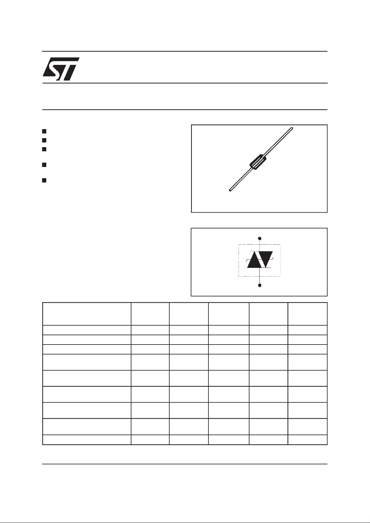
theCB429 axial package.
TRISILdevices provide bidirectional protectionby
crowbar action. Their characteristic response to
transient overvoltages makes them particularly
suitedtoprotect voltage sensitive telecommunicationequipment.
CB429
SCHEMATIC DIAGRAM
TRISIL
TM
COMPLIESWITHTHE
FOLLOWING STANDARDS:
CCITTK20
VDE0433 4000 10/700 5/310 100 VDE0878 4000 1.2/50 1/20 100 IEC-1000-4-5 level4
FCCPart 68, lightningsurge
typeA
FCCPart 68, lightningsurge
typeB
BELLCORETR-NWT-001089
Firstlevel
BELLCORETR-NWT-001089
Secondlevel
CNETl31-24 4000 0.5/700 0.8/310 100 -
October 1998 - Ed: 6A
Peak Surge
Voltage
(V)
4000 10/700 5/310 100 -
level4
1500
800
100 5/320 5/320 25 -
2500
1000
500 2/10 2/10 500 -
Voltage
Waveform
(µs)
10/700
1.2/50
10/160
10/560
2/10
10/1000
Current
Waveform
(µs)
5/310
8/20
10/160
10/560
2/10
10/1000
Admissible
Ipp
(A)
100
100
200
100
500
100
Necessary
Resistor
(Ω)
-
-
-
-
-
-
1/5

TPB SERIES
ABSOLUTE MAXIMUM RATINGS(T
Symbol Parameter Value Unit
P Powerdissipationon infiniteheatsink T
I
PP
I
TSM
2
tI
I
Peak pulsecurrent 10/1000µs
Non repetitivesurge peak on-statecurrent tp = 20 ms 50 A
2
t valueforfusing tp = 20 ms 25 A2s
dV/dt Criticalrate of riseof off-statevoltage V
T
stg
T
j
T
L
Storagetemperaturerange
Maximumjunctiontemperature
Maximumleadtemperaturefor soldering during 10s at 5mm for
case
THERMALRESISTANCES
Symbol Parameter Value Unit
(j-l) Junctionto leads(L
R
th
(j-a)
R
th
Junctionto ambient on printed circuit(L
lead
ELECTRICAL CHARACTERISTICS
(T
=25°C)
amb
=25°C)
amb
=50 °C5 W
amb
100
8/20 µs
2/10 µs
RM
150
500
5kV/µs
- 55 to+ 150
150
230 °C
= 10mm) 20 °C/W
lead
= 10 mm)
75 °C/W
A
°C
°C
Symbol Parameter
V
RM
I
RM
V
V
BR
V
BO
I
H
I
BO
I
PP
C
Type I
TPB62
TPB68
TPB100
TPB120
TPB130
TPB180
TPB200
TPB220
TPB240
TPB270
Note 1: IRmeasuredat VRguarantees V
Note 3: See test circuit 2. Note 4: V
2/5
Stand-offvoltage
Leakagecurrentat stand-offvoltage
ContinuousReverse voltage
R
Breakdownvoltage
Breakovervoltage
Holdingcurrent
Breakovercurrent
Peakpulse current
Capacitance
@V
RM
RM
max. max.
AV
µ
2
2
2
2
2
2
2
2
2
2
56
61
90
108
117
162
180
198
216
243
BRmin≥VR
IR@V
R
max.
note1
AV VmAmApF
µ
50
50
50
50
50
50
50
50
50
50
62
68
100
120
130
180
200
220
240
270
note2
82
90
133
160
173
240
267
293
320
360
Note 2: Measured at 50 Hz (1 cycle) - See test circuit 1.
VBO@I
BO
I
H
min.
note3
800
800
800
800
800
800
800
800
800
800
= 1V, F = 1MHz, refer tofig.3 for C versus V
R
150
150
150
150
150
150
150
150
150
150
C
max.
note4
300
300
200
200
200
200
200
200
200
200
R.
 Loading...