

SGS Thomson Microelectronics TODV640, TODV1240, TODV1040, TODV840 Datasheet
FEATURES
.HIGHCOMMUTATION: > 142A/ms (400Hz)
.INSULATINGVOLTAGE= 2500V
(ULRECOGNIZED: EB1734)
.HIGH VOLTAGECAPABILITY: V
DESCRIPTION
The TODV 640 ---> 1240 use a high performance
passivated glass alternistor technology. Featuring
very high commutation levels and high surge current capability, this family is well adapted to power
control on inductive load (motor, transformer...)
(RMS)
DRM
=1200 V
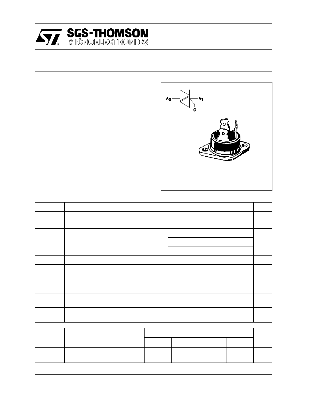
TODV 640 ---> 1240
ALTERNISTORS
A
2
G
A
1
RD91
(Plastic)
ABSOLUTE RATINGS (limitingvalues)
Symbol Parameter Value Unit
I
T(RMS)
I
TSM
I2tI
dI/dt Critical rate of rise of on-state current
Tstg
Tj
Tl Maximum lead temperature for soldering during 10 s at 4.5 mm
Symbol Parameter TODV Unit
RMS on-state current
(360° conduction angle)
Non repetitive surge peak on-state current
( Tj initial = 25°C)
2
t value tp = 10 ms 610 A2s
Gate supply : IG= 500mA diG/dt = 1A/µs
Storage and operating junction temperature range - 40 to + 150
from case
640 840 1040 1240
Tc = 75 °C40 A
tp = 2.5 ms 590 A
tp = 8.3 ms 370
tp = 10 ms 350
Repetitive
F = 50 Hz
Non
Repetitive
20 A/µs
100
- 40 to + 125
260 °C
°C
°C
V
DRM
V
RRM
March 1995
Repetitive peak off-state voltage
Tj = 125 °C
600 800 1000 1200 V
1/5
TODV 640 ---> 1240
THERMAL RESISTANCES
Symbol Parameter Value Unit
Rth (c-h) Contact (case-heatsink) with grease 0.1 °C/W
Rth (j-c) DC Junction to case for DC 1.2 °C/W
Rth (j-c) AC Junction to case for 360° conduction angle ( F= 50 Hz) 0.9 °C/W
GATECHARACTERISTICS (maximumvalues)
P
G (AV)
ELECTRICAL CHARACTERISTICS
=1W PGM= 40W (tp = 20 µs) IGM=8A(tp=20µs) VGM= 16V (tp = 20 µs).
Symbol Test Conditions Quadrant Value Unit
I
GT
V
GT
V
GD
tgt VD=V
I
L
IH*I
VTM*ITM= 60A tp= 380µs Tj=25°C MAX 1.8 V
I
DRM
I
RRM
dV/dt * Linear slope up to VD=67%V
(dI/dt)c * (dV/dt)c = 200V/µs Tj=125°C MIN 35 A/ms
* For either polarity of electrode A2voltage with reference to electrode A1.
VD=12V (DC) RL=33Ω Tj=25°C I-II-III MAX 200 mA
VD=12V (DC) RL=33Ω Tj=25°C I-II-III MAX 1.5 V
VD=V
DRMRL
DRMIG
dIG/dt = 3A/µs
IG=1.2 I
= 500mA gate open Tj=25°C TYP 50 mA
T
V
DRM
V
RRM
gate open
(dV/dt)c = 10V/µs 142
=3.3kΩ Tj=125°C I-II-III MIN 0.2 V
= 500mA
GT
Rated
Rated
DRM
Tj=25°C I-II-III TYP 2.5 µs
Tj=25°C I-III TYP 100 mA
II 200
Tj=25°C MAX 0.02 mA
Tj=125°C MAX 8
Tj=125°C MIN 500 V/µs
2/5
 Loading...