

SGS Thomson Microelectronics TL074M, TL074IN, TL074ID, TL074ACN, TL074CN Datasheet
...
TL07 4
LOW NOISE J-FET QUAD OPERATIONAL AMPLIFIERS
.WIDE COMMON-MODE (UP TO V
DIFFERENTIALVOLTAGERANGE
CC
+
)AND
.LOW INPUTBIASANDOFFSETCURRENT
.LOW NOISE e
=15nV/√Hz(typ)
n
.OUTPUTSHORT-CIRCUIT PROTECTION
.HIGH INPUT IMPEDANCE J–FET INPUT
STAGE
.LOW HARMONIC DISTORTION:0.01%(typ)
.INTERNALFREQUENCY COMPENSATION
.LATCHUPFREE OPERATION
.HIGHSLEWRATE : 13V/µs (typ)
TL074A - TL074B
N
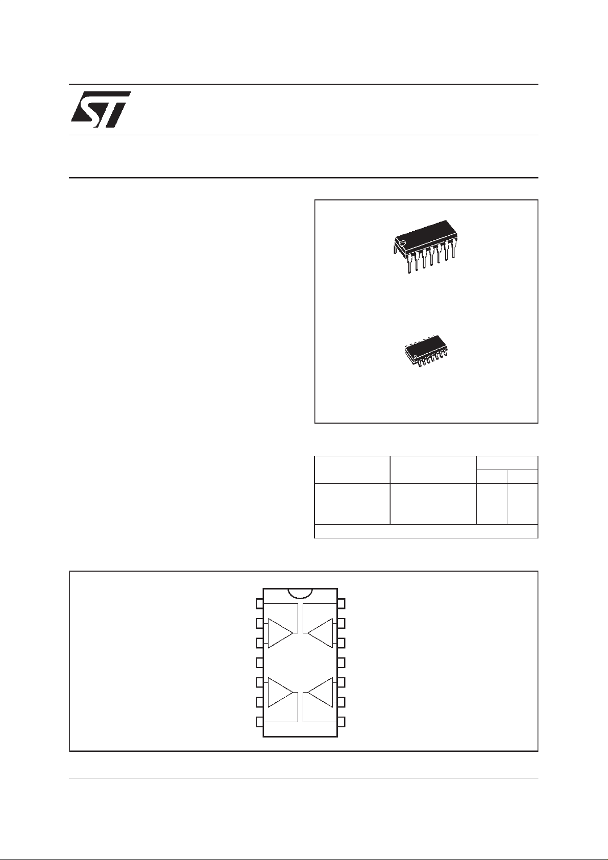
DIP14
(PlasticPackage)
D
SO14
(PlasticMicropackage)
DESC RIP TI ON
The TL074,T L074Aand TL074Bar ehi ghspeed
J–FETinputquadoper ati onalampli fi ersinc or porating
wellm atc hed,highv oltageJ–F ETand bipolartransistorsinamonolithicintegratedcircuit.
Thedev i c esfeaturehighslewrates,lowinputbiasand
offsetcurrents,andlow offsetvol t agetemperature
coefficient.
PIN CONNECTI O NS (topview)
Output 1
Inverting Input 1
Non-inverting Input 1
Non-inverting Input 2
Inverting Input 2
Output 2
1
2
-
+
3
+
4
V
CC
5
+
-
6
7
ORDER CODES
Part Number
TL074M/AM/BM –55
TL074I/AI/BI –40
TL074C/AC/BC 0
Example : TL074IN
14
Output 4
13
-
+
+
-
Inverting Input 4
12
Non-inverting Input 4
11
10
9
8
-
V
CC
Non-inverting Input 3
Inverting Input 3
Output 3
Temperature
Range
o
C, +125oC ••
o
C, +105oC ••
o
C, +70oC ••
Package
ND
December 1998
1/10
TL074 - TL074A - TL074B
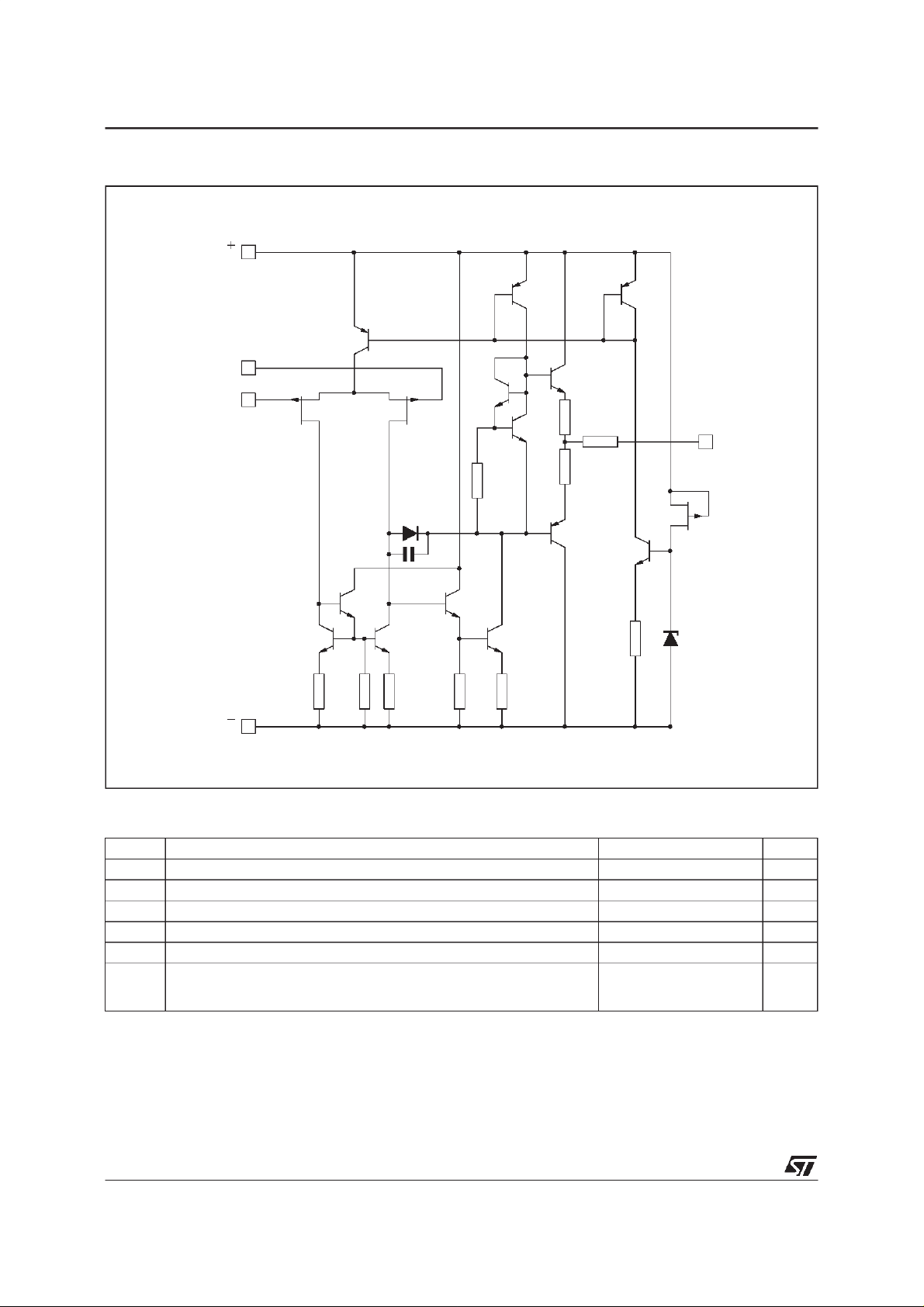
SCHEMATI C DIAGRAM
V
CC
Non -inverting
inp ut
Inverting
input
V
CC
1.3k
35k
1.3k
35k
30k
10 0
100
Ω10 0
Ω
Ω
200
8.2k
Ω
Output
1/4 TL074
ABSOLUTE MAXIMUM RATINGS
Symbol Parameter Value Unit
V
T
Notes : 1. All voltage values,exceptdifferentialvoltage, are withrespect to the zero reference level (ground) ofthe supplyvoltages where the
2/10
Supply Voltage - (note 1) ±18 V
CC
Input Voltage - (note 3) ±15 V
V
i
Differential Input Voltage - (note 2) ±30 V
V
id
Power Dissipation 680 mW
P
tot
Output Short-circuit Duration - (note 4) Infinite
Operating Free Air Temperature Range TL074C,AC,BC
oper
TL074I,AI,BI
TL074M,AM,BM
zero referencelevel isthe midpointbetween V
2. Differentialvoltages are atthe non-inverting inputterminal withrespect tothe invertinginput terminal.
3. The magnitude of theinput voltage mustneverexceed the magnitude of the supply voltage or 15 volts, whichever is less.
4. The outputmay be shorted to ground or toeither supply. Temperature and /orsupply voltages mustbe limited toensure thatthe
dissipation ratingis notexceeded.
+
CC
andV
–
.
CC
0to70
–40 to 105
–55 to 125
o
C

TL074 - TL074A - TL074B
ELECTRICAL CHARACTERISTICS
= ±15V, T
V
CC
Symbol Parameter
V
DV
A
Input Offset Voltage (RS=50Ω)
io
Input Offset Voltage Drift 10 10 µV/oC
io
Input Offset Current *
I
io
Input Bias Current *
I
ib
Large Signal Voltage Gain (RL=2kΩ,VO=±10V)
vd
SVR Supply Voltage Rejection Ratio (R
I
V
Supply Current, per Amp, no Load
CC
Input Common Mode Voltage Range ±11 +15
icm
CMR Common Mode Rejection Ratio (R
Ios Output Short-circuit Current
±V
Output Voltage Swing
OPP
SR Slew Rate (V
T
amb
t
Rise Time (Vin= 20mV, RL=2kΩ,CL= 100pF,
r
T
amb
K
Overshoot (Vin= 20mV, RL=2kΩ,CL= 100pF,
OV
T
amb
GBP Gain Bandwidth Product (f = 100kHz,
T
amb
R
Input Resistance 10
i
THD Total Harmonic Distortion (f = 1kHz, A
R
L
Equivalent Input Noise Voltage
e
n
(f = 1kHz, R
∅m Phase Margin 45 45 Degrees
V
O1/VO2
* The inputbias currents arejunction leakage currents whichapproximately double for every 10oC increasein the junctiontemperature.
Channel Separation (Av= 100) 120 120 dB
=25oC (unless otherwise specified)
amb
TL074I,M,AC,AI,
AM,BC,BI,BM
Min. Typ. Max. Min. Typ. Max.
=25oC TL074
T
T
T
T
T
T
T
T
T
T
T
T
amb
min.
amb
min.
amb
min.
amb
min.
amb
min.
amb
min.
≤ T
amb
=25oC
≤ T
amb
=25oC
≤ T
amb
=25oC
≤ T
amb
=25oC
≤ T
amb
=25oC
≤ T
amb
≤ T
≤ T
≤ T
≤ T
≤ T
≤ T
max.
max.
max.
max.
max.
max.
TL074A
TL074B
TL074
TL074A
TL074B
=50Ω)
S
5025200 2515200
808086 707086
3
10
3
1
13
5 100
20 200
20
1.4 2.5
2.5
6
3
7
5
4
±11 +15
-12
=50Ω)
=25oC
T
amb
≤ T
T
min.
T
amb
T
min.
T
amb
T
min.
=25oC, unity gain) 8 13 8 13
≤ T
amb
max.
=25oC
≤ T
≤ T
amb
max.
=25oCR
≤ T
≤ T
amb
max.
= 10V, RL=2kΩ, CL= 100pF,
in
S
=2kΩ
L
= 10kΩ
R
L
RL=2kΩ
= 10kΩ
R
L
808086 707086
101040 6060101040 60
10
12
10
12
12
13.5
10
12
10
12
=25oC, unity gain) 0.1 0.1
=25oC, unity gain) 10 10
=25oC, Vin= 10mV, RL=2kΩ,CL= 100pF) 2 3 2 3
12
= 20dB,
=2kΩ,CL= 100pF, T
= 100Ω)
s
=25oC, VO=2VPP) 0.01 0.01
amb
V
15 15
TL074C
310
5 100
30 200
1.4 2.5
-12
12
13.5
12
10
13
10
20
2.5
60
Unit
mV
pA
nA
pA
nA
V/mV
dB
mA
V
dB
mA
V
V/µs
µs
%
MHz
Ω
%
nV
√Hz
3/10
 Loading...