

SGS Thomson Microelectronics TL064ID, TL064I, TL064M, TL064IN, TL064ACD Datasheet
...
LOW POWER J-FET QUAD OPERATIONAL AMPLIFIERS
■
VERYLOWPOWER CONSUMPTION : 200µA
■
WIDE COMMON-MODE (UP TO V
DIFFERENTIALVOLTAGERANGES
■
LOW INPUTBIAS AND OFFSETCURRENTS
■
OUTPUTSHORT-CIRCUIT PROTECTION
■
HIGH INPUT IMPEDANCE J-FET INPUT
STAGE
■
INTERNAL FREQUENCYCOMPENSATION
■
LATCHUP FREE OPERATION
■
HIGH SLEW RATE: 3.5V/µs
CC
+
) AND
TL064
TL064A - TL064B
DESCRIPTION
The TL064, TL064Aand TL064B are high speed
J-FET input quad operational amplifiers. Each of
these J-FET input operational amplifiers incorporateswellmatched, highvoltage J-FETand bipolar
transistorsin a monolithicintegrated circuit.
The device featureshigh slewrate, low input bias
and offsetcurrents,andlowoffsetvoltagetemperature coefficient.
PIN CONNECTIONS(top view)
Output 1
Inverting Input 1
Non-inverting Input 1
Non-inverting Input2
Inverting Input 2
Output 2
1
2
-
+
3
+
V
4
CC
5
+
-
6
7
N
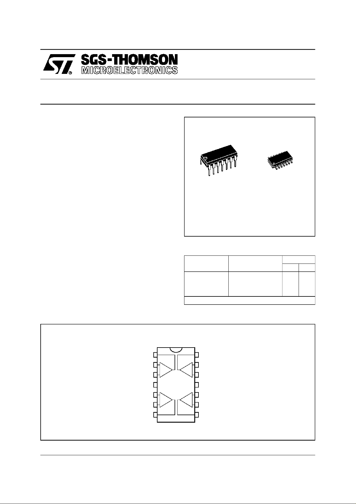
DIP14
(Plastic Package)
(Plastic Micropackage)
ORDER CODES
Part Number Temperature Range
o
TL064M/AM/BM -55
TL064I/AI/BI -40
TL064C/AC/BC 0
Example : TL064IN
14
Output 4
13
-
+
+
-
Inverting Input 4
12
Non-inverting Input 4
-
V
11
CC
10
Non-inverting Input 3
9
Inverting Input 3
8
Output 3
C, +125oC ••
o
C, +105oC ••
o
C, +70oC ••
D
SO14
Package
ND
October 1997
1/10
TL064 - TL064A - TL064B
SCHEMATIC DIAGRAM
220Ω
V
CC
Inverting
Input
4.2k
Ω
Non-inverting
Input
45k
100Ω
Output
64
Ω
1/4 TL064
Ω
270Ω
3.2k
Ω
V
CC
MAXIMUMRATINGS
Symbol Parameter TL064M,AM,BM TL064I,AI,BI TL064C,AC,BC Unit
V
V
P
T
T
Notes : 1. All voltage values, except differential voltage,are withrespect to thezero reference level (ground) of the supply voltages where
Supply Voltage -(note 1) ±18 ±18 ±18 V
CC
Input Voltage - (note3) ±15 ±15 ±15 V
V
i
Differential Input Voltage - (note 2) ±30 ±30 ±30 V
id
Power Dissipation 680 680 680 mW
tot
Output Short-Circuit Duration (Note4) Infinite Infinite Infinite
Operating Free-Air Temperature
oper
-55 to +125 -40 to +105 0 to +70
Range
Storage Temperature Range -65 to +150 -65 to +150 -65 to +150
stg
the zero reference level is themidpoint between V
+
CC
2. Differential voltages are the non-inverting input terminal with respect to the inverting input terminal.
3. The magnitudeof the input voltage must never exceed the magnitudeof the supply voltage or 15 volts, whicheveris less.
4. The outputmay be shorted toground or to either supply. Temperature and/orsupply voltages must be limited to ensure that the
dissipation rating is notexceeded.
and V
-
.
CC
o
C
o
C
2/10
TL064 - TL064A - TL064B
ELECTRICAL CHARACTERISTICS
=±15V,T
V
CC
Symbol Parameter
Input Offset Voltage(Rs=50Ω)
V
io
DV
Temperature Coefficient of Input
io
Offset Voltage (R
Input OffsetCurrent*
I
io
Input Bias Current*
I
ib
V
Input Common Mode Voltage
icm
Range
V
Output Voltage Swing (RL= 10kΩ)
OPP
A
Large Signal Voltage Gain
vd
(R
L
GBP Gain Bandwidth Product
(T
amb
C
= 100pF)
L
Input Resistance 10
R
i
CMR Common Mode Rejection Ratio
(R
s
SVR Supply Voltage Rejection Ratio
(R
s
Supply Current (Per Amplifier)
I
cc
(T
amb
V
O1/VO2
* The input bias currents ofa FET-input operational amplifier are normaljunction reverse currents, which are temperature sensitive.
Pulse techniques must be used thatwill maintain the junction temperatureas close to the ambient temperature as possible.
Channel Separation
(A
v
Total Power Consumption
P
D
(T
amb
=25oC (unless otherwise specified)
amb
=25oC
T
amb
T
. ≤ T
min
T
amb
. ≤ T
T
min
T
amb
T
min.
T
amb
T
. ≤ T
min
amb
=50Ω)
s
=25oC
amb
=25oC
≤ T
amb
=25oC
amb
≤ T
≤ T
≤ T
≤ T
max.
max.
max
max
.
.
= 10kΩ,Vo=±10V)
=25oC
T
amb
T
min
. ≤ T
amb
≤ T
max
.
=25oC, RL= 10kΩ
= 50Ω)
=50Ω)
=25oC, noload, no signal)
= 100,T
amb
=25oC)
=25oC, noload, no signal)
TL064M TL064I TL064C
Min. Typ. Max. Min. Typ. Max. Min. Typ. Max.
36
15
36
9
315
20
10 10 10
5 100
30 200
±11.5 +15
-12
20
50
±11.5 +15
5 100
10
30 200
20
-12
5 2005pA
30 40010pA
±11 +15
-12
202027 202027 202027
4
64
4
63
4
6
3
111
12
10
12
10
12
80 86 80 86 70 76
80 95 80 95 70 95
200 250 200 250 200 250
120 120 120
6 7.5 6 7.5 6 7.5
Unit
mV
µV/
nA
nA
V
V
V/mV
MHz
Ω
dB
dB
µA
dB
mW
o
C
ELECTRICAL CHARACTERISTICS (continued)
=±15V,T
V
CC
Symbol Parameter
SR Slew Rate (V
Rise Time (Vi= 20mV,RL= 10kΩ,CL= 100pF, AV= 1) (see Figure 1) 0.2 µs
t
r
K
Overshoot Factor (Vi= 20mV, RL= 10kΩ,CL= 100pF, AV=1)
OV
(see figure 1)
Equivalent Input Noise Voltage
e
n
(R
s
=25oC
amb
= 10V, RL= 10kΩ,CL= 100pF, AV= 1) 1.5 3.5 V/µs
i
= 100Ω, f = 1KHz)
TL064C,I,M
Min. Typ. Max.
10
42
Unit
%
nV
√Hz
3/10
 Loading...