

SGS Thomson Microelectronics TL061CN, TL061C, TL061CD, TL061ACN, TL061ACD Datasheet
...
LOW POWERJ-FET SINGLE OPERATIONAL AMPLIFIER
.
VERYLOW POWERCONSUMPTION : 200µA
.
WIDE COMMON-MODE (UP TO V
DIFFERENTIAL VOLTAGE RANGES
.
LOW INPUT BIAS AND OFFSETCURRENTS
.
OUTPUTSHORT-CIRCUIT PROTECTION
.
HIGH INPUT IMPEDANCE J-FET INPUT
STAGE
.
INTERNAL FREQUENCY COMPENSATION
.
LATCHUP FREEOPERATION
.
HIGHSLEWRATE : 3.5V/µs
CC
+
) AND
TL061A - TL061B
N
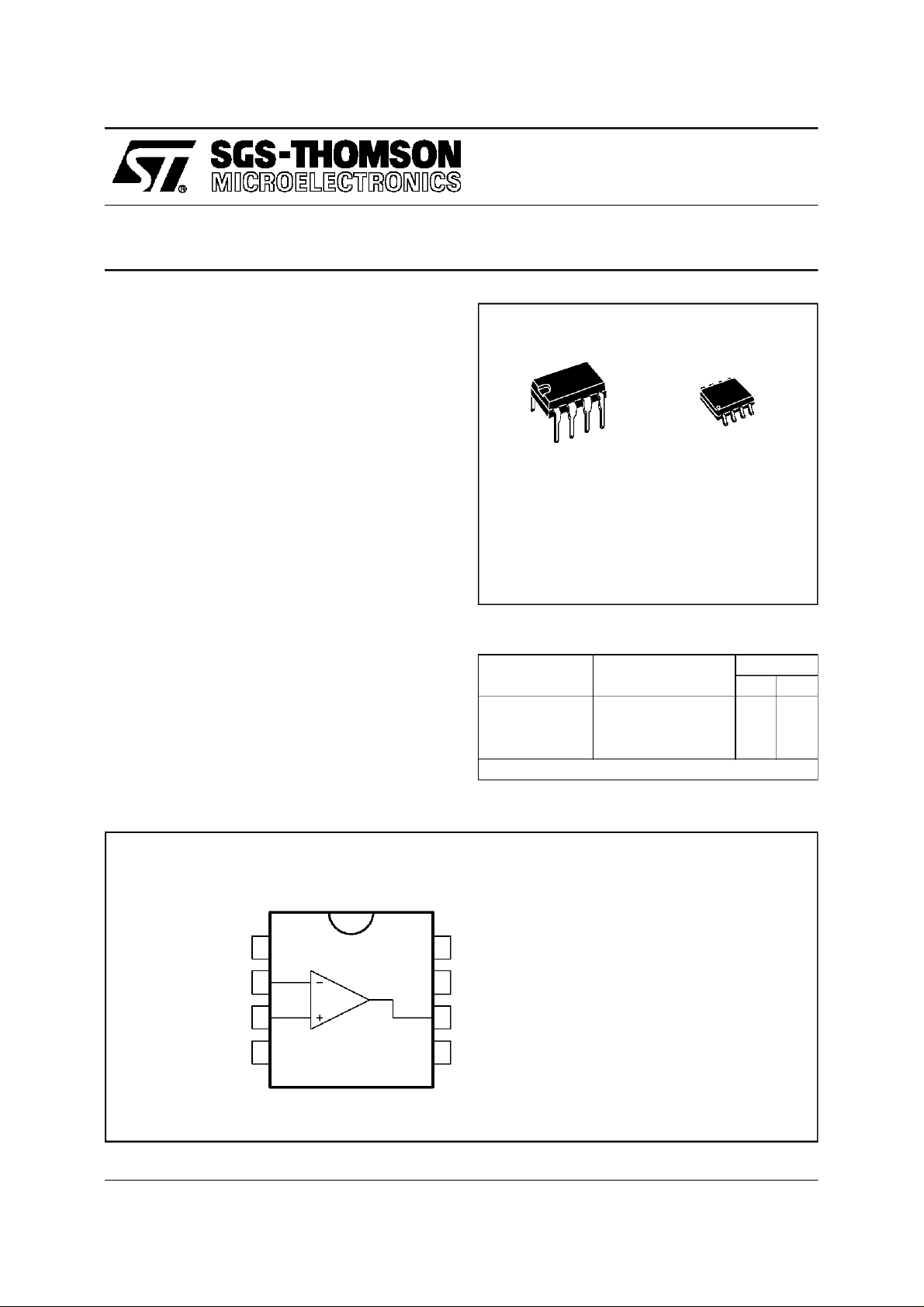
DIP8
(Plastic Package)
TL061
D
SO8
(Plastic Micropackage)
DESCRIPTION
The TL061, TL061A and TL061B are high speed
J-FET input single operational amplifier family.
Each of these J-FET input operational amplifiers
incorporateswellmatched,highvoltageJ-FETand
bipolartransistorsin a monolithicintegratedcircuit.
The devicesfeature highslew rates, low inputbias
and offsetcurrents,andlow offsetvoltagetemperature coefficient.
PIN CONNECTIONS(top view)
1
2
3
4
ORDER CODES
Part Number Temperature Range
o
TL061M/AM/BM -55
TL061I/AI/BI -40oC, +105oC ● l
TL061C/AC/BC 0
Example : TL061IN
1 - Offset Null1
8
7
6
5
2 - Inverting input
3 - Non-inverting input
-
4-V
CC
5 - Offset Null2
6 - Output
+
7-V
CC
8 - N.C.
C, +125oC ●●
o
C, +70oC ● l
Package
ND
October 1997
1/9
TL061 - TL061A - TL061B
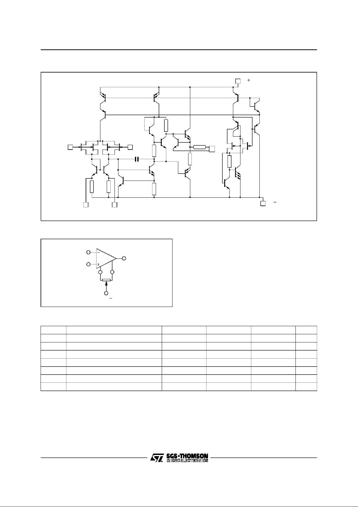
SCHEMATIC DIAGRAM
220 Ω
V
CC
Inverting
Input
Offset Null 1 Offset Null 2
4.2k Ω
Non-inverting
Input
INPUT OFFSET VOLTAGE NULL CIRCUIT
TL061
N1 N2
100k Ω
V
CC
45k Ω
100 Ω
270
64Ω
Output
Ω
3.2k Ω
V
CC
MAXIMUMRATINGS
Symbol Parameter TL061M,AM,BM TL061I,AI,BI TL061C,AC,BC Unit
V
V
P
T
T
Notes : 1. All voltagevalues, exceptdifferential voltage, are withrespect to thezero reference level (ground) of the supply voltages where
2/9
Supply Voltage - (note 1) ±18 ±18 ±18 V
CC
Input Voltage - (note 3) ±15 ±15 ±15 V
V
i
Differential Input Voltage - (note 2) ±30 ±30 ±30 V
id
Power Dissipation 680 680 680 mW
tot
Output Short-Circuit Duration (Note 4) Infinite Infinite Infinite
Operating Free-Air TemperatureRange -55 to +125 -40 to +105 0 to +70
oper
Storage TemperatureRange - 65 to + 150 -65 to + 150 - 65 to + 150
stg
the zero reference level is the midpoint between V
2. Differentialvoltages are thenon-inverting input terminal with respect to the invertinginput terminal.
3. The magnitude of the input voltage must neverexceed the magnitude of the supply voltage or 15 volts, whichever is less.
4. The outputmay be shorted to ground or to either supply. Temperature and/or supply voltages must be limited toensure that the
dissipation rating is notexceeded.
+
CC
and V
-
.
CC
o
C
o
C
TL061 - TL061A- TL061B
ELECTRICAL CHARACTERISTICS
=±15V,T
V
CC
Symbol Parameter
Input Offset Voltage(Rs=50Ω)
V
io
DV
V
V
TemperatureCoefficient of Input
io
Offset Voltage (R
I
Input OffsetCurrent *
io
Input Bias Current *
I
ib
Input Common Mode Voltage
icm
Range
Output Voltage Swing (RL= 10kΩ)
OPP
A
Large Signal VoltageGain
vd
(R
L
GBP Gain Bandwidth Product
(T
amb
= 100pF) 1 1 1
C
L
Input Resistance 10
R
i
CMR Common Mode Rejection Ratio
(R
s
SVR Supply Voltage Rejection Ratio
(R
s
I
Supply Current
cc
(T
amb
P
TotalPower Consumption
D
(T
amb
* The input bias currents of a FET-input operationalamplifier are normal junction reverse currents, which are temperature sensitive.
Pulse techniques must be used that will maintain the junction temperature as close to the ambient temperature as possible.
=25oC (unless otherwise specified)
amb
TL061M TL061I TL061C
Min. Typ. Max. Min. Typ. Max. Min. Typ. Max.
T
T
T
T
T
T
T
T
amb
min
amb
min
amb
min.
amb
min
=25oC
. ≤ T
=25oC
. ≤ T
=25oC
≤ T
amb
=25oC
. ≤ T
≤ T
amb
max.
=50Ω)101010
s
≤ T
amb
max.
≤ T
.
max
±11.5 +15
≤ T
max
.
amb
36
9
5 100
20
30 200
50
±11.5 +15
-12
36
9
5 100
10
30 200
20
-12
30 40010pA
±11 +15
-12
202027 202027 202027
315
5 2005pA
= 10kΩ,Vo=±10V)
T
T
amb
min
=25oC
. ≤ T
amb
≤ T
max
.
4
64
63
4
6
3
4
=25oC, RL= 10kΩ
12
10
12
10
12
= 50Ω) 8086 8086 7076
=50Ω) 8095 8095 7095
=25oC, no load, no signal) 200 250 200 250 200 250
=25oC, no load, no signal) 6 7.5 6 7.5 6 7.5
20
Unit
mV
µV/
nA
nA
V
V
V/mV
MHz
Ω
dB
dB
µA
mW
o
C
ELECTRICAL CHARACTERISTICS (continued)
=±15V,T
V
CC
Symbol Parameter
SR Slew Rate (V
Rise Time (Vi= 20mV, RL= 10kΩ,CL= 100pF, AV= 1) 0.2 µs
t
r
K
Overshoot Factor (Vi= 20mV, RL= 10kΩ,CL= 100pF,AV=1)
OV
(see figure 1) 10
e
Equivalent Input Noise Voltage
n
(R
s
=25oC
amb
= 10V, RL= 10kΩ,CL= 100pF,AV= 1) 1.5 3.5 V/µs
i
= 100Ω, f = 1KHz) 42
TL061C,I,M
Min. Typ. Max.
Unit
%
nV
√Hz
3/9
 Loading...