

I2C BUS CONTROLLED 130MHz RGB PREAMPLIFIER
.
130MHz TYPICAL BANDWIDTH AT 2V
OUTPUTWITH12pF CAPACITIVELOAD
.
2.8ns TYPICAL RISE/FALL TIME AT 2V
OUTPUTWITH12pF CAPACITIVELOAD
.
POWERFULLOUTPUTDRIVE CAPABILITY
.
BRT, CONT, DRIVE, OUTPUT DC LEVEL,
OSD CONTRAST, BACK-PORCH CLAMPING
PULSE WIDTH ARE I
.
INTERNAL BACK-PORCH CLAMPING
PULSE GENERATOR
.
OSD WHITE BALANCETRACKING
.
INTERNAL OSD SWITCHES
.
BLANKINGAND FAST-BLANKING INPUTS
.
VERY LARGE DRIVE ADJUSTMENT RANGE
(48dB)
.
SEMI-TRANSPARENT BACKGROUND ON
OSDPICTURE
2
C BUS CONTROLLED
TDA9206
PP
PP
DIP24
(Plastic Package)
ORDER CODE : TDA9206
DESCRIPTION
The TDA9206 is a digitaly controlled wideband
video preamplifier intendedfor use in high resolution colormonitor.All controlsand adjustmentsare
digitaly performed thanks to I
trast, brightness and DC output level of RGB signals are common to the 3 channels and drive
adjustmentisseparateforeachchannel.ThreeI
gain controlled OSD inputs can be switched with
RGB signalsusingfastblankingcommand.Clamping of RGBsignalsis performedthanksto a flexible
integrated system. The white balance adjustment
is effectiveon brightness, videoand OSDsignals.
TheTDA9206works forapplicationusingACorDC
coupledCRTdriver.
Because of its features and due to component
savingtheTDA9206leadstoaveryperformantand
cost effectiveapplication.
2
C serial bus. Con-
2
C
PIN CONNECTIONS
IN1
OSD1
AV
IN2
OSD2
AGND
IN3
OSD3
LV
LGND
SDA
SCL
DD
DD
1
2
3
4
5
6
7
8
9
10
11
12
24
23
22
21
20
19
18
17
16
15
14
13
HSYNC
PV
CC1
OUT1
PGND1
PV
CC2
OUT2
PGND2
PV
CC3
OUT3
PGND3
BLK
FBLK
9206-01.EPS
September 1996
1/12
TDA9206
PIN DESCRIPTION
Name Pin Type Function
IN1 1 I 1
OSD1 2 I 1
AV
3 I 12V Analog V
DD
IN2 4 I 2ndChannel Main Picture Input
OSD2 5 I 2
AGND 6 I/O Analog Ground
IN3 7 I 3
OSD3 8 I 3
LV
9 I 12V Logic V
DD
LGND 10 I/O Logic Ground
SDA 11 I/O Serial Data Line
SCL 12 I Serial Clock Line
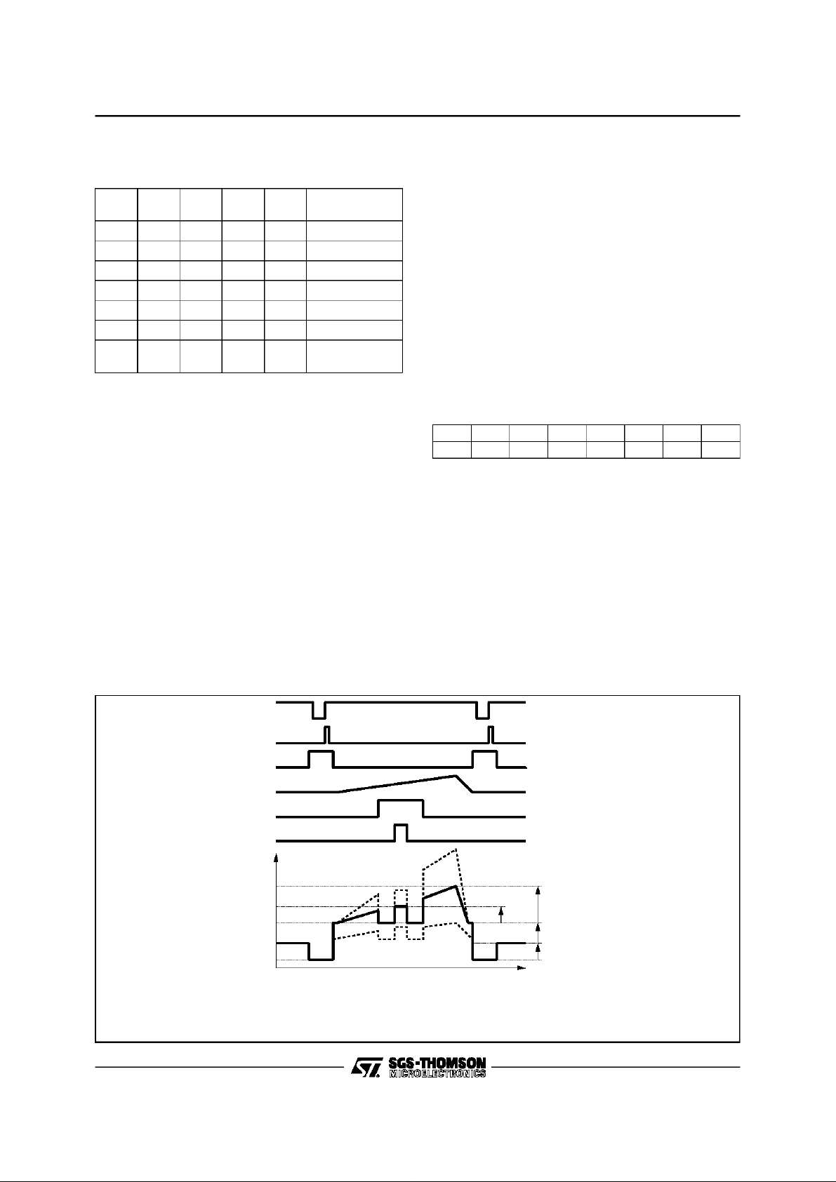
BLOCK DIAGRAM
st
Channel Main Picture Input
st
Channel OSD Input
DD
nd
Channel OSD Input
rd
Channel Main Picture Input
rd
Channel OSD Input
DD
Name Pin Type Function
FBLK 13 I Fast Blanking Input
BLK 14 I Blanking Input
rd
PGND3 15 I/O 3
OUT3 16 O 3
PV
17 I 3rdChannel Power V
CC3
Channel Power Ground
rd
Channel Output
CC
PGND2 18 I/O 2ndChannel Power Ground
nd
OUT2 19 O 2
PV
20 I 2ndChannel Power V
CC2
Channel Output
CC
PGND1 21 I/O 1stChannel Power Ground
st
OUT1 22 O 1
PV
23 I 1stChannel Power V
CC1
Channel Output
CC
HSYNC 24 I Horizontal Synch Input
9206-01.TBL
AV
IN1
AGND
IN2
IN3
LV
LGND
DD
DD
3
1
6
4
7
9
10
TDA9206
V
REF
BLUE CHANNEL
GREEN CHANNEL
BPCP
24
LATCHES
I
BUS
DECODER
11 12
CLAMP
2
C
SCLSDAHSYNC
FBLKBLK
CO NTRAST
D/A
OSD
CONT
1314
BRIGHTNESS
2
OSD1 OSD2 OSD3
5
DRIVE
8 bits
8
2
C
I
BPCP
OUTPUT
STAGE
V
REF
PV
CC1
23
OUTPUT
DC LEVEL
ADJUS T
22
21
20
19
18
16
17
15
OUT1
PGND1
PV
CC2
OUT2
PGND2
OUT3
PV
CC3
PGND3
9206-02.EPS
2/12

FUNCTIONAL DESCRIPTION
Input Stage
The R, G and B signals must be fed to the three
inputs through coupling capacitors (100nF).
The maximuminput peak-to-peakvideo amplitude
is 1V.
The inputstage includes a clampingfunction. This
clamp is using the input serialcapacitoras”memory capacitor”and is gatedby an internally generated ”Back-Porch-Clamping-Pulse(BPCP)”.
The synchronizationedge ofthe BPCP is selected
according bit 0 of registerR8.
When B0R8 is set to 1, the BPCP is synchronized
on the leading edge of the blanking pulse BLK
inputs on Pin 14 (see Figure1).
Figure1
BLK
HSYNC
BPCP
Internal pulse width is controlledby I2C
WhenB0R8isclearto0, the BPCPissynchronized
on the secondedgeofthehorizontalpulseHSYNC
inputs on Pin 24. An automatic function allows to
use positiveor negativehorizontal pulse on Pin 24
(see Figure2).
Figure2
HSYNC
BPCP
Internalpulse width is controlled by I2C
2
In both caseBPCP width is adjustable by I
C, B1
and B2 of register R8 (see R8 Table P8).
ContrastAdjustment (8 bits)
The contrast adjustment is made by controlling
simultaneously the gain of three internal variable
gain amplifiers through the I
2
C bus interface.
The contrast adjustment allows to cover a typical
range of 48dB.
BrightnessAdjustment (8 bits)
As for the contrast adjustment, the brightness is
controlledby I
2
C.
The brightness function consists to add the same
DC offsetto the threeR, G,Bsignals after contrast
amplification.
TDA9206
ThisDC-Offsetis presentonly outsidethe blanking
pulse (see Figure 3).
The DC output level during the blanking pulse, is
forced to ”INFRA-BLACK” level (V
Drive Adjustment (3 x 8 bits)
In orderto adjustthe white balance , the TDA9206
offersthe possibilityto adjustseparatelytheoverall
gain of each complete video channel.
The gainof each channelis controlledby I
each).
The verylargedriveadjustmentrange(48dB) allows
differentstandardor customcolortemperature.
It can also be used to adjust the output voltagesat
the optimum amplitude to drive the C.R.T drivers,
keepingthewholecontrastcontrolforend-useronly.
The drive adjustment is located after the CONTRAST, BRIGHTNESSandOSDswitch blocks,so
that the white balance will remains correct when
BRT is adjusted, and will also be correct on OSD
portion of the signal.
OSD Inputs
The TDA9206 includes all the circuitry necessary
9206-04.EPS
tomixOSDsignalsintotheRGBmain-picture.Four
pins are dedicatedto this function as follow.
Three TTL RGB On Screen Display inputs
(Pin 2, 5and 8). Thesethree inputs areconnected
to the three outputs of the corresponding ONSCREEN-DISPLAYprocessor(ex : STV942x).
One Fast Blanking Input (FBLK, Pin 13) which is
also connected to the FBLK output of the same
ON-SCREEN-DISPLAYprocessor.
When a high level is present on FBLK, the IC will
actsas follow :
- The three main picture RGB input signals are
internally switched to the internal input clamp
referencevoltage.
- The three output signals are set to voltages
9206-05.EPS
corresponding to the state (0 or 1) on the three
OSD inputs (see Figure 3).
Example:
If FBLK = 1 and OSD1, OSD2, OSD3) = 1, 0, 1
respectively.
Then OUT1, OUT2, OUT3 will be equal to V
V
BRT,VOSD
where : V
,
BRT=VBLACK
V
OSD=VBRT
+BRT
+OSD
BRTis the brightness DC level I
OSD is the On-Screen Display signal value I
adjustablefrom 0V to 4.68V
PP
Semi-transparent function is controlled thanks to
Bit6 of R8 register(see Table1).
When semi-transparent mode is activated, video
signalis dividedby 2 (CONT).
).
DC
2
2
C adjustable.
by step of 0.312V.
C (8bits
OSD
2
C
3/12
,
TDA9206
FUNCTIONAL DESCRIPTION(continued)
Table1
FBLK OSD1 OSD2 OSD3 B6R8
0 x x x 0 Video
1 x x x 0 OSD (1)
0 x x x 1 Video
10xx1 OSD
1 x 1 x 1 OSD
1 x x 0 1 OSD
1 1 0 1 1 Semi-trans-
Notes : 1. AllOSD colors are displayed.
2. One OSD color is displayed as semi-transparent video
without effect on brightnessand DC level adjustment.
Output Stage
Thethreeoutputstagesincorporatethreefunctions
which are :
- The blankingstage : When high level is applied
to the BLK input (Pin 14), the threeoutputs are
switchedtoa voltagewhichis 400mV lower than
the BLACK level. The black level is the output
voltage with minimum brightness when input
signalvideo amplitudeis equal to ”0”.
- The output stage itself : It is a large bandwidth
output amplifierwhich allow to deliver up to 5V
on the three outputs(for0.7V videosignal on the
inputs).Thetypicalbandwidth is 100MHzat -3dB
measuredwith 4V
output signalon 12pF load.
PP
Figure 3 : WaveformsVOUT, BRT, CONT, OSD
Output
Signal (OUTn)
parent (2)
PP
- The output CLAMP : The IC also incorporates
three internal output clamp (sample and hold
system) which allow to DC shift the three output
signals. The DC output voltage is adjustable
through I
2
C with 4 bits. Practicaly, the DC output
level allow to adjustthe BLKlevel
= 400mV under V
(V
DC
) from 0.9V to 2.9V
BLACK
with 12 x 165mV.
The overall waveforms of the output signal according to the different adjustment are shown in
Figures3 and 4.
Serial Interface
The 2-wiresserial interface is an I
2
C interface.
The slaveaddressof the TDA9206 is DC (in hexadecimal).
A6 A5 A4 A3 A2 A1 A0 W
11011100
Data Transfer
The host MCU can write data into the TDA9206
registers.Read mode is not available.
To write data into the TDA9206, after a start, the
MCU must send (see Figure 5) :
2
- TheI
Caddressslavebytewitha lowlevelfor the
R/W bit.
- The byte of the internal register address where
the MCU wants to write data(s).
- The data.
All bytes are sent MSB bit first and the write data
transteris closedby a stop.
4/12
HSYNC
BPCP
BLK
Video IN
FBLK
OSD IN
V
OUT1,VOUT2,VOUT3
(4)
V
CONT
(5)
V
OSD
(3)
V
BRT
(2)
V
BLACK
(1)
V
DC
Notes : 1. VDC= 0.5 to 2.5V
2. V
BLACK=VDC
3. V
BRT=VBLACK
4. V
CONT=VBRT
5. V
OSD=VBRT
CONT
OSD
BRT
0.4V fixed
+ 0.4V
+ BRT (with BRT= 0 to 2.5V)
+ CONT with CONT = k x Video IN (CONT = 5VPPmax. for VIN= 0.7VPP)
+ OSD with OSD = k1 x OSDIN (OSD max. = 5VPP, OSD min. = 312mVPP)
9206-06.EPS

FUNCTIONAL DESCRIPTION(continued)
Figure 4 : Waveforms(DRIVE adjustment)
HSYNC
BP CP
BLK
Video IN
FBLK
OSD IN
V
OUT1,VOUT2,VOUT3
V
OSD
V
TDA9206
CONT
V
BRT
V
BLACK
V
DC
1. Drive adjustment modifies the following voltages : V
Note :
Drive a djustment do not modifythe following voltage s : V
Two examples
of drive adjustment
(1)
and V
CONT,VBRT
DC
and V
BLACK
OSD
.
.
Figure 5 : I2C WriteOperation
SCL
SDA
W
2
C Slave AddressStart
A7 A6 A5 A4 A3 A2 A1 A0
Register Address ACKACKI
D7 D6 D5 D4 D3 D2 D1 D0
Data Byte ACK Stop
QUICK REFERENCE DATA
Symbol Parameter Min. Typ. Max. Unit
Signal Bandwidth (2V
Rise and Fall Time (2V
Drive Adjustment Range on the 3 Channels separately 48 dB
Maximum Output Voltage (V
Output Voltage Range (AC + DC) 8 V
/12pF load) 130 MHz
PP
/12pF load) 2.8 ns
PP
= 0.7 VPP)5V
IN
9206-07.EPS
9206-08.EPS
9206-02.TBL
5/12

TDA9206
ABSOLUTEMAXIMUM RATINGS
Symbol Parameter Value Unit
V
V
V
V
T
T
THERMALDATA
Supply Voltage (Pins 3-9-17-20-23) 14 V
S
Voltage at any Input Pins (except SDA & SCL)
IN1
Voltage at any Input Pins (on SDA & SCL)
IN2
ESD Susceptability (Human body model ; 100pF Discharge through 1.5kΩ)2kV
ESD
Storage Temperature - 40, + 150 °C
stg
Junction Temperature 150 °C
T
j
Operating Temperature 0, + 70 °C
oper
GND < V
GND < V
IN1<VS
< 5.5VV
IN2
9206-03.TBL
Symbol Parameter Value Unit
R
th (j-a)
Junction-ambient Thermal Resistance 62
DC ELECTRICALCHARACTERISTICS (T
=25oC, VCC=12V, unless otherwise specified)
amb
o
Symbol Parameter Test Conditions Min. Typ. Max. Unit
Supply Voltage Pins 3-9-17-20-23 11.4 12 12.6 V
S
Supply Current (All VSPin current) RL=1kΩ 90 mA
I
S
Video Input Voltage Amplitude Pins 1-4-7 0.7 1 V
I
Typical Output Voltage Range Pins 16-19-22 0.5 - 8 V
O
Low Level Inputs OSD, FBLK, BLK,HSYNC Pins 2, 5, 8, 13, 14, 24 0.8 V
High Level Inputs OSD, FBLK, BLK, HSYNC Pins 2, 5, 8, 13, 14, 24 2.4 V
V
IL OSD
V
IH OSD
V
V
V
AC ELECTRICALCHARACTERISTICS
=25oC, VCC= 12V,CL= 12pF,RL=1kΩ , unless otherwisespecified)
(T
amb
Symbol Parameter Test Conditions Min. Typ. Max. Unit
AV MaximumGain (20 log x V
OUT AC/VIN AC
CAR Contrast Attenuation Range V
DAR Drive Attenuation Range V
GM Gain Match V
BW
Bandwidth Large Signal
Bandwidth Small Signal
DIS Video Output Distorsion (see Note) f = 1MHz, V
t
R,tF
Video Output Rise and Fall Time
(see Note)
BRT Brightness Maximum DC Level
Brightness Minimum DC Level
BRTM Brightness Matching BRT = 50%, Drive = POR ± 20 mV
Note : POR = Power-on Reset Value
) Contrast & Drive at maximum 18 dB
= 0.7V, BRT, Drive = POR 48 dB
IN
= 0.7V, Contrast, Drive = POR 48 dB
IN
= 2.5VPP,VIN= 0.7V
OUT
Contrast = Drive = Maxi x 0.7 (POR)
At -3dB, V
V
Contrast = Drive = Maxi x 0.87
V
Contrast = Drive = Maxi x 0.62
OUT
OUT
= 0.7V
IN
=4VPP,
=2VPP,
=1VPP,VIN=1V
OUT
PP
PP
PP
± 0.1 dB
100
130
0.3 %
VIN= 0.7VPP,
3.8
=4V
V
OUT
Contrast = Drive = Maxi x 0.87
V
OUT
Contrast = Drive = Maxi x 0.62
=2V
PP
PP
4.5 ns
2.8
2.5
0
C/W
PP
MHz
MHz
ns
V
V
9206-04.TBL
9206-05.TBL
9206-06.TBL
6/12

TDA9206
AC ELECTRICALCHARACTERISTICS
=25oC, VCC= 12V,CL= 12pF,RL=1kΩ , unless otherwisespecified)
(T
amb
Symbol Parameter Test Conditions Min. Typ. Max. Unit
OSD
CAR
DC Output Maximum DC Level
CT Croostalkbetween Video Channels
Notes : 1. These parameters are not tested on each unit. They are measured during an internal qualification procedure which includes
2
C ELECTRICAL CHARACTERISTICS (T
I
Symbol Parameter Test Conditions Min. Typ. Max. Unit
f
SCL(Max.)
Contrast Attenuation Range
for OSD Input
Output Minimum DC Level
Equivalent Load on Video Output with Tj≤ T
R
L
(see Note 1)
characterization on batches coming from corners of our processes and also from temperature characterization.
2. POR = Power-on Reset Value
V
IL
V
IH
I
IN
Low LevelInput Voltage On Pins SDA, SCL 1.5 V
High LevelInput Voltage 3 V
Input Current 0.4V < VIN< 4.5V -10 +10 µA
SCL Maximum Clock Frequency 200 kHz
V
OL
Low LevelOutput Voltage SDA Pin when ACK
j Max.
= 2.5VPP,VIN= 0.7V
V
OUT
Contrast = Drive = Maxi x 0.7 (POR)
= 1MHz
f
IN
= 50MHz
f
IN
=25oC, VCC= 12V, unlessotherwise specified)
amb
PP
0.47 1 kΩ
44
34
Sink Current = 6mA
24 dB
2.5
0.5
dB
dB
0.6 V
V
V
9206-07.TBL
9206-08.TBL
I2C INTERFACE TIMINGS REQUIREMENTS (See Figure6)
Symbol Parameter Min. Typ. Max. Unit
t
BUF
t
HDS
t
SUP
t
LOW
t
HIGH
t
HDAT
t
SUDAT
t
R,tF
Time the bus must be free between 2 access 1300 ns
Hold Time for Start Condition 600 ns
Set-up Time for Stop Condition 600 ns
The Low Period of Clock 1300 ns
The High Period of Clock 600 ns
Hold Time Data 300 ns
Set-up Time Data 250 ns
Rise and Fall Time of both SDA and SCL 20 300 ns
Figure6
SDA
SCL
t
HDS
t
BUF
t
HIGH
t
SUDAT
t
HDAT
t
SUP
t
LOW
9206-09.TBL
9206-09.EPS
7/12

TDA9206
REGISTERDESCRIPTION
Registers Sub-address
Address (Hex) Register Names Function POR Value
01 Contrast DAC 8-bit B4
02 Brightness DAC 8-bit B4
03 Drive 1 DAC 8-bit B4
04 Drive 2 DAC 8-bit B4
05 Drive 3 DAC 8-bit B4
06 Output DC Level DAC 4-bit 08
07 OSD Contrast DAC 4-bit 08
08 BP and Miscellaneous See R8 Table 04
Contrast Register (R1) (Video IN = 0.5VPP, Brightnessat minimum,Drive at maximum)
Hex b7 b6 b5 b4 b3 b2 b1 b0 CONT (VPP) G (dB) POR Value
00 00000000 0 01 0 0 0 0 0 0 0 1 0.015 -30
02 0 0 0 0 0 0 1 0 0.031 -24
04 0 0 0 0 0 1 0 0 0.062 -18
08 0 0 0 0 1 0 0 0 0.125 -12
10 0 0 0 1 0 0 0 0 0.25 -6
20 0 0 1 0 0 0 0 0 0.5 0
40 01000000 1 6
80 10000000 2 12
B4 1 0 1 1 0 1 0 0 2.812 15 X
FF 11111111 4 18
BrightnessRegister (R2) (Driveat maximum)
Hex b7 b6 b5 b4 b3 b2 b1 b0 BRT (V) POR Value
00 00000000 0
01 0 0 0 0 0 0 0 1 0.010
02 0 0 0 0 0 0 1 0 0.020
04 0 0 0 0 0 1 0 0 0.040
08 0 0 0 0 1 0 0 0 0.080
10 0 0 0 1 0 0 0 0 0.160
20 0 0 1 0 0 0 0 0 0.320
40 0 1 0 0 0 0 0 0 0.640
80 1 0 0 0 0 0 0 0 1.28
B4 1 0 1 1 0 1 0 0 1.8 X
FF 1 1 1 1 1 1 1 1 2.56
8/12
TDA9206
REGISTERDESCRIPTION (continued)
Drive Registers(R3, R4, R5) (VideoIN = 0.5V
Hex b7 b6 b5 b4 b3 b2 b1 b0 CONT (VPP) G (dB) POR Value
00 00000000 0 -
01 0 0 0 0 0 0 0 1 0.015 -30
02 0 0 0 0 0 0 1 0 0.031 -24
04 0 0 0 0 0 1 0 0 0.062 -18
08 0 0 0 0 1 0 0 0 0.125 -12
10 0 0 0 1 0 0 0 0 0.25 -6
20 0 0 1 0 0 0 0 0 0.5 0
40 01000000 1 6
80 10000000 2 12
B4 1 0 1 1 0 1 0 0 2.812 15 X
FF 11111111 4 18
Output DC LevelRegister (R6)
Hex b7 b6 b5 b4 b3 b2 b1 b0 DC (V) POR Value
03 0 0 0 0 0 0 1 1 0.52
04 0 0 0 0 0 1 0 0 0.69
08 0 0 0 0 1 0 0 0 1.35 X
0F 00001111 2.5
Code 00Hex, 01Hex and 02Hex :not to be used
, Brightnessatminimum,Contrast at maximum)
PP
OSD Contrast Register (R7) (V
Hex b7 b6 b5 b4 b3 b2 b1 b0 OSD (V) G (dB) POR Value
00 00000000 0 -
01 0 0 0 0 0 0 0 1 0.312 -24
02 0 0 0 0 0 0 1 0 0.625 -18
04 0 0 0 0 0 1 0 0 1.25 -12
08 0 0 0 0 1 0 0 0 2.5 -6 X
0F 0 0 0 0 1 1 1 1 4.68 0
OSD IN
= 2.4V
.., Drive at maximum)
Min
BP and MiscellaneousRegister (R8)
b7 b6 b5 b4 b3 b2 b1 b0 Function POR Value
0 BP Source = HSYNC X
1 BP Source = BLK
0 0 BP Pulse Width = 0.33µs
0 1 BP Pulse Width = 0.66µs
1 0 BP Pulse Width = 1µsX
1 1 BP Pulse Width = 1.3µs
0 0 Test Purposes X
0 0 0 Soft Blanking OFF X
1 1 1 Soft Blanking ON
0 Semi Transparent OFF X
1 Semi Transparent ON
Unused
9/12

TDA9206
INTERNALSCHEMATICS
Figure7
AV
DD
IN
Pins
1-4-7
AGND
Figure8
OSD - BLK- FBLK
Pins 2-5-8-13-14
AV
DD
Figure9
Figure11
AV
AGND
DD
3
(20V)
6
10LGND
AV
DD
AGND
LGND
9206-10.EPS
Figure10
9206-12.EPS
Figure12
11-12
SDA
SCL
Pins
LV
AGND
DD
(10V)
AGND AGND
AV
DD
9
AGND
9206-11.EPS
9206-13.EPS
Figure13
HSYNC
10/12
24
AV
DD
AGND
AGND
LGND
9206-14.EPS
Figure14
Pins 17-20-23
Pins 15-18-21
9206-16.EPS
PV
PGND
LGND
CC
AV
DD
OUT
Pins 16-19-22
AGND
9206-15.EPS
9206-17.EPS

APPLICATION DIAGRAM
SYNCHRO
EXTRACTOR
TDA9206
+5V
33pF
8MHz
GND B
GND R
GND G
100nF
B
R
G
33pF
FBLK
1
VSYNC
2
HSYNC
3
V
4
5
PXCK
6
CKOUT
7
XTALOUT
XTALIN
8
+12V
100nF
47
Ω
1kΩ
75
Ω
100nF
47
Ω
1k
75Ω
100nF
47
Ω
75
Ω
16
TEST
15
GND
RESET
SDA
SCL
B
14
G
13
R
12
11
10
9
S
T
DD
V
9
4
2
6
+5V
10µF
16V
100nF
1k
100nF
Ω
2.7k
1
2
OSD1
3
AV
DD
IN2
4
Ω
Ω
OSD2
5
AGND
6
IN3
7
OSD3
8
LV
9
DD
LGND
10
SDA
11
SCL
12 13
GND GND
100
Ω
1kΩ
22pF
HSYNC
PV
CC1
OUT1
PGND1
T
D
PV
OUT2
PGND2
PV
OUT3
PGND3
BLK
FBLK
SDA
SCL
CC2
CC3
I
A
9
2
0
6
24IN1
23
22
21
20
19
18
17
16
15
14
2
C BUS
100nF
100nF
100nF
BLK
HSYNC
VSYNC
BLUE OUT
RED OUT
GREEN OUT
9206-18.EPS
11/12

TDA9206
PACKAGE MECHANICAL DATA
24 PINS- PLASTICDIP
Dimensions
Min. Typ. Max. Min. Typ. Max.
Millimeters Inches
a1 0.63 0.025
b 0.45 0.018
b1 0.23 0.31 0.009 0.012
b2 1.27 0.050
D 32.2 1.268
E 15.2 16.68 0.598 0.657
e 2.54 0.100
e3 27.94 1.100
F 14.1 0.555
i 4.445 0.175
L 3.3 0.130
Information furnished is believed to be accurate and reliable. However, SGS-THOMSON Microelectronics assumes no responsibility
for the consequences of use of such information nor for anyinfringement of patents or other rights of third parties which may result
from its use. Nolicence is granted by implication or otherwise under any patent or patent rights of SGS-THOMSON Microelectronics.
Specifications mentioned in this publication are subject to change without notice. This publication supersedes and replaces all
information previously supplied. SGS-THOMSON Microelectronics products are not authorized for use as critical components in life
support devices or systems without express written approval of SGS-THOMSON Microelectronics.
1996 SGS-THOMSON Microelectronics - All Rights Reserved
Purchase of I
2
I
C Patent. Rights to use these components in a I2C system, is granted provided that the system conformsto
Australia - Brazil -Canada - China - France - Germany - Hong Kong - Italy - Japan - Korea - Malaysia - Malta - Morocco
The Netherlands - Singapore - Spain - Sweden - Switzerland - Taiwan - Thailand - United Kingdom - U.S.A.
2
C Components of SGS-THOMSON Microelectronics, conveys a license under the Philips
2
the I
C Standard Specifications as defined by Philips.
SGS-THOMSON Microelectronics GROUP OF COMPANIES
PM-DIP24.EPS
DIP24.TBL
12/12
 Loading...