

TDA9109A
LOW-COST I2C CONTROLLED DEFLECTION PROCESSOR
FOR MULTISYNC MONITOR
FEATURES
General
■ SYNC PROCESSOR
■ 12V SUPPLY VOLTAGE
■ 8V REFERENCE VOLTAGE
■ HORIZONTAL LOCK/UNLOCK OUTPUT
■ READ/WRITE I
■ VERTICAL MOIRE
■ B+ REGULATOR
- Internal PWM generator for B+ current mode
step-up converter
- Switchable to step-down converter
-I2C adjustable B+ reference voltage
- Output Pulses Synchronized on Horizontal
Frequency
- Internal Maximum Current Limitation
Horizontal
■ Self-adaptative
■ Dual PLL concept
■ 150kHz maximum frequency
■ X-ray protection input
2
■ I
C controls:
Horizontal duty-cycle, H-position
2
C INTERFACE
DESCRIPTION
The TDA9109A is a monolithic integrated circuit
assembled in a 32-pin shrink dual in line plastic
package. This IC controls all the functions related
to the horizontal and vertical deflection in multimode or multi-frequency computer display monitors.
The internal sync processor, combined with the
very powerful geometry correction block, make
the TDA9109A suitable for very high performance
monitors, using very few external components.
The horizontal jitter level is very low. It is particularly well-suited to high-end 15” and 17” monitors.
Combined with the ST7275 Microcontroller family,
TDA9206 (Video preamplifier) and STV942x (OnScreen Display controller), the TDA9109A allows
fully I2C bus-controlled computer display monitors
to be built with a reduced number of external components
.
Vertical
■ Vertical ramp generator
■ 50 to 185Hz AGC loop
■ Geometry tracking with Vpos & Vamp
2
■ I
C controls:
SHRINK32 (Plastic Package)
ORDER CODE: TDA9109A
Vamp, Vpos, S-corr, C-corr
■ DC breathing compensation
I2C Geometry corrections
■ Vertical parabola generator
(Pin Cushion - E/W, Keystone, Corner
Correction)
■ Horizontal dynamic phase
(Side Pin Balance & Parallelogram)
■ Horizontal and vertical dynamic focus
(Horizontal focus amplitude, Horizontal focus
symmetry, Vertical focus amplitude)
Version 4.2
June 2000 1/47
1

TABLE OF CONTENTS
PIN CONNECTIONS 4
PIN CONNECTIONS 5
QUICK REFERENCE DATA 6
BLOCK DIAGRAM 8
ABSOLUTE MAXIMUM RATINGS 9
THERMAL DATA 9
I2C READ/WRITE 10
SYNC PROCESSOR 10
HORIZONTAL SECTION 11
VERTICAL SECTION 13
DYNAMIC FOCUS SECTION 15
GEOMETRY CONTROL SECTION 16
B+ SECTION 18
TYPICAL OUTPUT WAVEFORMS 20
I2C BUS ADDRESS TABLE 24
I2C BUS ADDRESS TABLE 25
OPERATING DESCRIPTION 27
1 GENERAL CONSIDERATIONS . . . . . . . . . . . . . . . . . . . . . . . . . . . . . . . . . . . . . . . . . . . . . . . 27
1.1Power Supply . . . . . . . . . . . . . . . . . . . . . . . . . . . . . . . ........................... 27
1.2I2C Control . . . . . . . . . . . . . . . . . . . . . . . . . . . ................................. 27
1.3Write Mode . . . . . . . . . . . . ...............................................27
1.4Read Mode . .. . . . . . . . . . . . . . . . . ........................................ 27
1.5Sync Processor . . . . . . . . . . . . . . . . . . . . . . . ................................. 27
1.6Sync Identification Status ................................................ 28
1.7IC status . . . . . . . . . . . . . . . . . . . . . . . . . . . . . . ................................28
1.8Sync Inputs .. . . . . . . . . . . ...............................................28
1.9Sync Processor Output . . . . . . . . . . ........................................28
2 HORIZONTALPART . . . .................................................... 28
2.1Internal Input Conditions . . ............................................... 28
2.2PLL1 . . . . . . . . . . . . . . . . . . . . . . . . . . . . . . . ................................. 29
2.3PLL2 . . . . . . . . . . . . . . . . . . . . . . . . . . . . . . . ................................. 31
2.4Output Section . . . . . ....................................................32
2.5X-RAY Protection . . . . . . . . . . . . . . . ........................................32
2.6Horizontal and Vertical Dynamic Focus . . . . .................................. 33
3 VERTICAL PART . . . . . . .................................................... 34
3.1Function . .............................................................34
3.2I2C Control Adjustments . . . . . . . . . . . .. . . . . . . . . . . . . . . . . . . . . . . . . . . . . ........ 34
3.3Vertical Moiré . . . . . . . ................................................... 34
3.4Basic Equations . . . . . . . . . . . . . ........................................... 35
3.5E/W ................................................................. 36
3.6Dynamic Horizontal Phase Control . . . . . . . . . . . . . . . . . . . . . .................... 36
3
2/47
2

TABLE OF CONTENTS
4 DC/DC CONVERTER PART . . ............................................... 37
4.1Step-up Mode . . . ...................................................... 37
4.2Step-down Mode . . . . . . . . . . . . . . . . . . . . . . . . . .............................. 37
4.3Step-up and Step-down Mode Comparison . . ................................. 37
INTERNAL SCHEMATICS 39
PACKAGE MECHANICAL DATA 46
3/47
3
TDA9109A
PIN CONNECTIONS
H/HVIN
VSYNCIN
HLOCKOUT
PLL2C
C0
R0
PLL1F
HPOSITION
HFOCUSCAP
FOCUS-OUT
HGND
HFLY
HREF
COMP
1
2
3
4
5
6
7
8
9
10
11
12
13
14
32
31
30
29
28
27
26
25
24
23
22
21
20
19
5V
SDA
SCL
V
CC
BOUT
GND
HOUT
XRAY
EWOUT
VOUT
VCAP
VREF
VAGCCAP
VGND
4/47
REGIN
I
SENSE
15
16
18
BREATH
B+GND17
TDA9109A
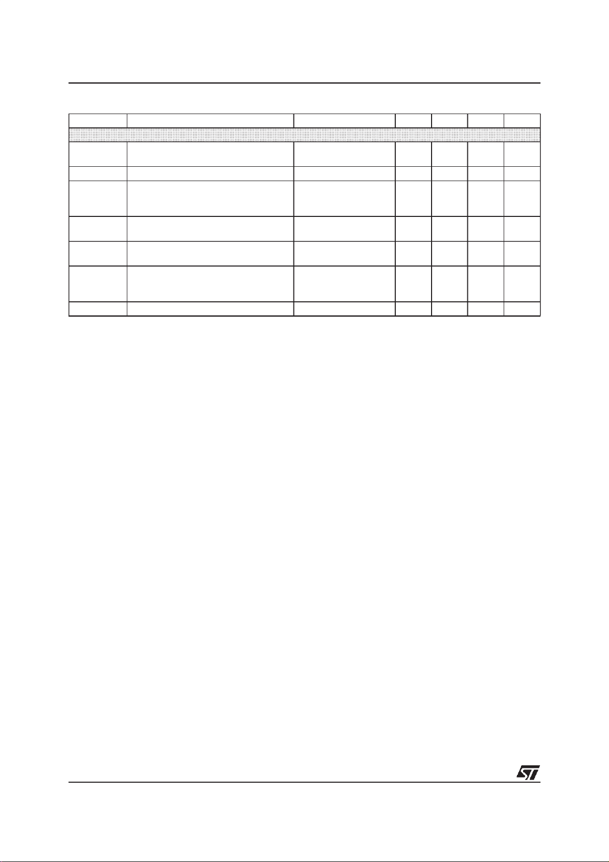
PIN CONNECTIONS
Pin Name Function
1 H/HVIN TTL compatible Horizontal sync Input (separate or composite)
2 VSYNCIN TTL compatible Vertical sync Input (for separated H&V)
3 HLOCKOUT First PLL Lock/Unlock Output (0 V: Unlocked - 5 V: Locked)
4 PLL2C Second PLL Loop Filter
5 C0 Horizontal Oscillator Capacitor
6 R0 Horizontal Oscillator Resistor
7 PLL1F First PLL Loop Filter
8 HPOSITION Horizontal Position Filter (capacitor to be connected to HGND)
9 HFOCUSCAP Horizontal Dynamic Focus Oscillator Capacitor
10 FOCUS OUT Mixed Horizontal and Vertical Dynamic Focus Output
11 HGND Horizontal Section Ground
12 HFLY Horizontal Flyback Input (positive polarity)
13 HREF Horizontal Section Reference Voltage (to be filtered)
14 COMP B+ Error Amplifier Output for frequency compensation and gain setting
15 REGIN Regulation Input of B+ control loop
16 I
SENSE
17 B+GND Ground (related to B+ reference adjustment)
18 BREATH DC Breathing Input Control (compensation of vertical amplitude against EHV variation)
19 VGND Vertical Section Ground
20 VAGCCAP Memory Capacitor for Automatic Gain Control Loop in Vertical Ramp Generator
21 V
REF
22 VCAP Vertical Sawtooth Generator Capacitor
23 VOUT
24 EWOUT Pin Cushion - E/W Correction Parabola Output
25 XRAY X-RAY protection input (with internal latch function)
26 HOUT Horizontal Drive Output (NPN open collector)
27 GND General Ground (referenced to V
28 BOUT B+ PWM Regulator Output
29 V
CC
30 SCL I
31 SDA I
32 5V Supply Voltage (5V typ.)
Sensing of external B+ switching transistor current,or switch for step-down converter
Vertical Section Reference Voltage (to be filtered)
Vertical Ramp Output (with frequency independant amplitude and S or C Corrections if
any). It is mixed with vertical position voltage and vertical moiré.
)
CC
Supply Voltage(12V typ)
2
C Clock Input
2
C Data Input
5/47
TDA9109A
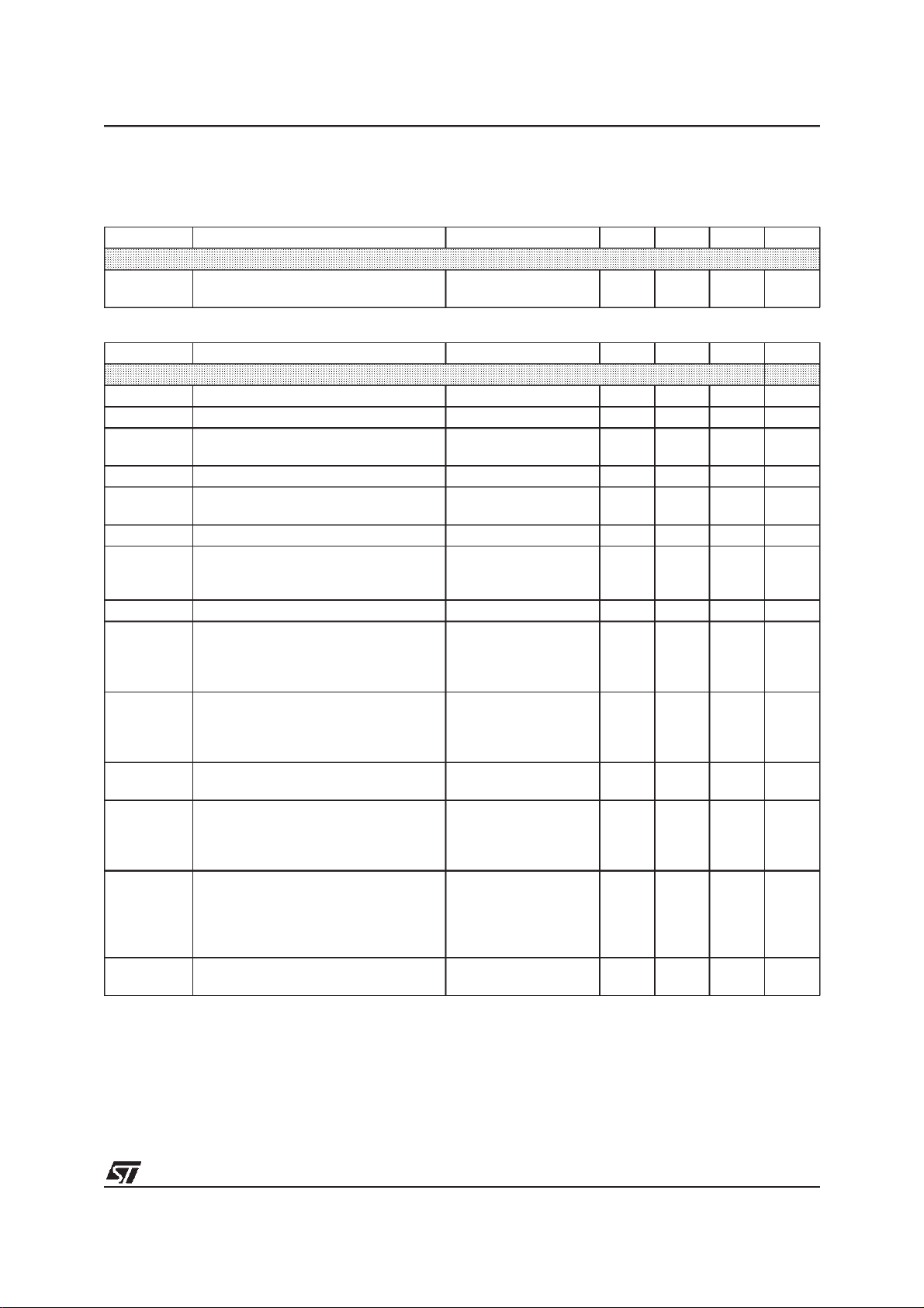
QUICK REFERENCE DATA
Parameter Value Unit
Horizontal Frequency 15 to 150 kHz
Autosynch Frequency (for given R0 and C0. Can be easily increased by application) 1 to 4.5 f0
± Horizontal Sync Polarity Input YES
Polarity Detection (on both Horizontal and Vertical Sections) YES
TTL Composite Sync YES
Lock/Unlock Identification (on both Horizontal 1st PLL and Vertical Section) YES
2
C Control for H-Position ±10 %
I
XRAY Protection YES
2
C Horizontal Duty Cycle Adjustment 30 to 65 %
I
2
C Free Running Frequency Adjustment NO
I
Stand-by Function YES
Dual Polarity H-Drive Outputs NO
Supply Voltage Monitoring YES
PLL1 Inhibition Possibility NO
Blanking Outputs NO
Vertical Frequency 35 to 200 Hz
Vertical Autosync (for 150nF on Pin 22 and 470nF on Pin 20) 50 to 185 Hz
Vertical S-Correction (optimized for super flat tube) YES
Vertical C-Correction YES
Vertical Amplitude Adjustment YES
DC Breathing Control on Vertical Amplitude YES
Vertical Position Adjustment YES
East/West (E/W) Parabola Output (also known as Pin Cushion Output) YES
E/W Correction Amplitude Adjustment YES
Keystone Adjustment YES
Corner Correction with Amplitude Adjustment YES
Internal Dynamic Horizontal Phase Control YES
Side Pin Balance Amplitude Adjustment YES
Parallelogram Adjustment YES
Tracking of Geometric Corrections with Vertical Amplitude and Position YES
Reference Voltage (both on Horizontal and Vertical) YES
Dynamic Focus (both Horizontal and Vertical) YES
2
C Horizontal Dynamic Focus Amplitude Adjustment YES
I
2
C Horizontal Dynamic Focus Symmetry Adjustment YES
I
2
C Vertical Dynamic Focus Amplitude Adjustment YES
I
6/47

Parameter Value Unit
Detection of Input Sync (biased from 5V alone) YES
Vertical Moiré YES
Controlled V-Moiré Amplitude YES
Frequency Generator for Burn-in NO
2
C Read/Write 400 kHz
Fast I
2
B+ Regulation adjustable by I
CYES
Horizontal Size Control NO
TDA9109A
7/47
8/47
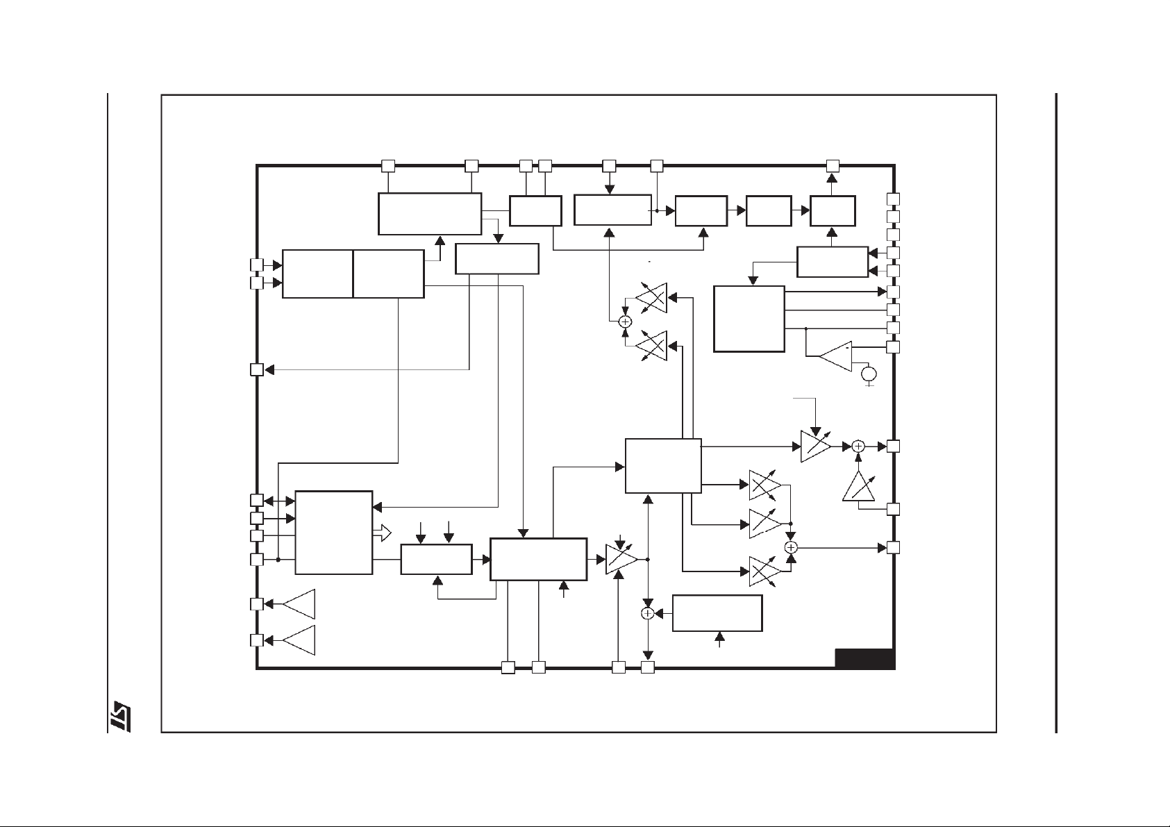
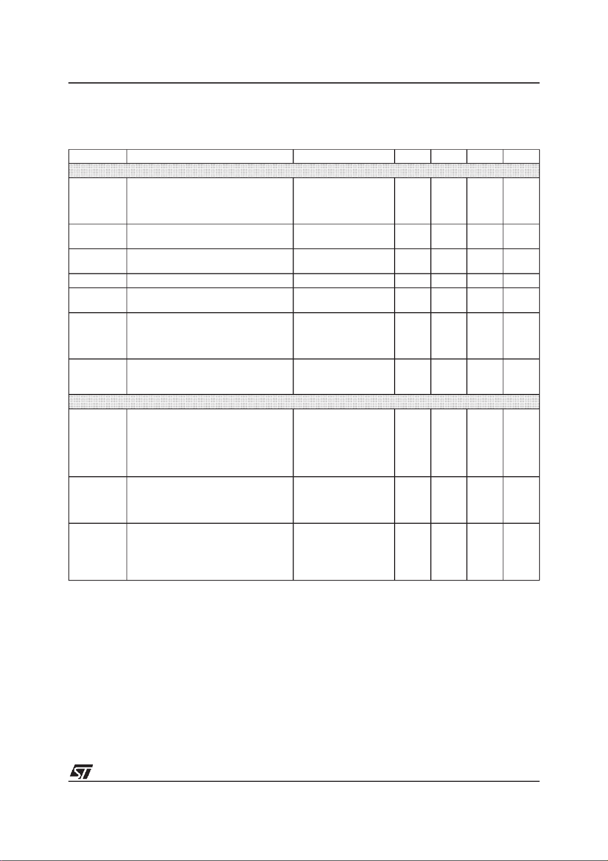
H/HVIN
SYNCIN
V
HLOCKOUT
SDA
SCL
GND
5V
1
2
3
31
30
27
32
SyncInput
Select
(1bit)
2
I
C Interface
PLL1F POSITION R0 C0 HFLY PLL2C HOUT
7 8 6 5 12 4 26
Phase/Frequency
Comparator
H-Phase(7bits)
Sync
Processor
VCO
Lock/Unlock
Identification
Phase
Comparator
SPinbal
7bits
2
x
Phase
Shifter
H-Duty
(7bits)
Safety
Processor
B+
Controller
x
Paral
7bits
VDFAMP
7bits
2
4
2
x
x
Amp
Symmetry
2x7bits
7 bits7 bits
S andC
Correction
Vertical
Oscillator
RampGenerator
VAMP
7bits
Geometry
Tracking
E/Wpcc
7bits
Keyst.
7 bits
Corner
7bits
x
x
Hout
Buffer
+
5V
Internal
reference
(7bits)
2
x
11
19
17
29
25
28
16
14
15
10
9
24
HGND
VGND
BGND
VCC
XRAY
BOUT
I
SENSE
COMP
REGIN
FOCUS
HFOCUSCAP
EWOUT
BLOCK DIAGRAM
TDA9109A
HREF
VREF
13
21
OUT
VerticalMoire
Cancel
7bits+ON/OFF
VSYNC
TDA9109A
H
ref
V
ref
VPOS
7bits
23182022
BREATHVAGCCAPVCAP
V
TDA9109A
ABSOLUTE MAXIMUM RATINGS
Symbol Parameter Value Unit
V
CC
V
DD
V
IN
Supply Voltage (Pin 29) 13.5 V
Supply Voltage (Pin 32) 5.7 V
Max Voltage on Pin 4
Pin 9
Pin 5
Pins 6, 7, 8, 14, 15, 16, 20, 22
Pins 10, 18, 23, 24, 25, 26, 28
Pins 1, 2, 3, 30, 31
4.0
5.5
6.4
8.0
V
V
CC
DD
ESD susceptibility Human Body Model, 100pF Discharge
VESD
T
stg
T
j
T
oper
through 1.5kΩ
EIAJ Norm, 200pF Discharge through 0Ω
2
300
Storage Temperature -40, +150 °C
Junction Temperature +150 °C
Operating Temperature 0, +70 °C
THERMAL DATA
Symbol Parameter Value Unit
R
th(j-a)
Max. Junction-Ambient Thermal Resistance 65 °C/W
V
V
V
V
V
V
kV
V
9/47
TDA9109A
I2C READ/WRITE
Electrical Characteristics (VDD= 5V, T
Symbol Parameter Test Conditions Min. Typ. Max. Units
2
C PROCESSOR (See1)
I
Fscl Maximum Clock Frequency Pin 30 400 kHz
Tlow Low period of the SCLClock Pin 30 1.3 µs
Thigh High period of the SCL Clock Pin 30 0.6 µs
Vinth SDA and SCL Input Threshold Pins 30, 31 2.2 V
VACK
2
C leak
I
Note: 1 See also I2C Bus Address Table.
Acknowledge Output Voltage on SDA
input with 3mA
Leakage current into SDA and SCL
with no logic supply
amb
=25°C)
Pin 31 0.4 V
V
=0
DD
Pins 30, 31 = 5 V
20 µA
SYNC PROCESSOR
Operating Conditions (VDD= 5V, T
Symbol Parameter Test Conditions Min. Typ. Max. Units
HsVR Voltage on H/HVIN Input Pin 1 0 5 V
MinD
Mduty
VsVR Voltage on VSYNCIN Pin 2 0 5 V
VSW Minimum Vertical Sync Pulse Width Pin 2 5 µs
VSmD
VextM
Minimum Horizontal Input Pulses Duration
Maximum Horizontal Input Signal Duty
Cycle
Maximum Vertical Sync Input Duty Cycle
Maximum Vertical Sync Width on TTL
H/Vcomposite
amb
=25°C)
Pin 1 0.7 µs
Pin 1 25 %
Pin 2 15 %
Pin 1 750 µs
Electrical Characteristics (VDD= 5V, T
Symbol Parameter Test Conditions Min. Typ. Max. Units
VINTH
RIN
VoutT
Note: 2 THis the Horizontal period.
10/47
Horizontal and Vertical Input Logic
Level (Pins 1, 2)
Horizontal and Vertical Pull-Up Resistor
Extracted Vsync Integration Time (%
) on H/V Composite (see2)
of T
H
amb
=25°C)
High Level
Low Level
Pins 1, 2 250 kΩ
C0 = 820pF 26 35 %
2.2
0.8
V
V
TDA9109A
HORIZONTALSECTION
Operating Conditions
Symbol Parameter Test Conditions Min. Typ. Max. Units
VCO
I
0max
F(max.) Maximum Oscillator Frequency 150 kHz
OUTPUT SECTION
I12m Maximum Input Peak Current Pin 12 5 mA
HOI
Max Current from Pin 6 Pin 6 1.5 mA
Horizontal Drive Output Maximum
Current
Pin 26, Sunk current 30 mA
Electrical Characteristics (VDD= 12V, T
amb
=25°C))
Symbol Parameter Test Conditions Min. Typ. Max. Units
SUPPLY AND REFERENCE VOLTAGES
V
V
I
I
V
REF-H
V
REF-V
I
REF-H
I
REF-V
CC
DD
CC
DD
Supply Voltage Pin 29 10.8 12 13.2 V
Supply Voltage Pin 32 4.5 5 5.5 V
Supply Current Pin 29 50 mA
Supply Current Pin 32 5 mA
Horizontal Reference Voltage Pin 13, I = -2mA 7.6 8.2 8.8 V
Vertical Reference Voltage Pin 21, I = -2mA 7.6 8.2 8.8 V
Max. Sourced Current on V
Max. Sourced Current on V
REF-H
REF-V
Pin 13 5 mA
Pin 21 5 mA
1st PLL SECTION
HpoIT
Delay Time for detecting polarity
change (see
3
)
Vvco VCO Control Voltage (Pin 7)
Vcog VCO Gain (Pin 7)
Hph
Vbmi
Vbtyp
Vbmax
IPII1U
IPII1L
f
o
Horizontal Phase Adjustment
4
)
(see
Horizontal Phase Setting Value (Pin 8)
4
)
(see
Minimum Value
Typical Value
Maximum Value
PLL1 Filter Current Charge
Free Running Frequency
Pin 1 0.75 ms
= 8.2V f
V
REF-H
fH(Max.)
= 6.49kΩ,
R
0
=820pF
C
0
% of Horizontal
Period
o
1.4
6.4
15.9 kHz/V
±10 %
Sub-Address 01
Byte x1111111
Byte x1000000
Byte x0000000
PLL1 is Unlocked
PLL1 is Locked
R
= 6.49kΩ,
0
= 820pF
C
0
2.9
3.5
4.2
±140
±1
22.8 kHz
Free Running Frequency Thermal Drift
dfo/dT
(No drift on external components)
5
)
(see
CR PLL1 Capture Range
fH(Min.)
fH(Max.) (See Note 6)
-150
f
o
4.5f
+0.5
o
HUnlock DC level pin 3 when PLL1 is locked 5 V
V
V
V
V
V
µA
mA
ppm/
C
kHz
kHz
11/47
TDA9109A
Symbol Parameter Test Conditions Min. Typ. Max. Units
2nd PLL SECTION AND HORIZONTAL OUTPUT SECTION
FBth
Hjit Horizontal Jitter (See
HDmin
HDmax
XRAYth
Vphi2
VSCinh
HDvd Horizontal Drive Output (low level) Pin 26, I
Note: 3 This delay is mandatory to avoid a wrong detection of polarity change in the case of a composite sync.
Note: 4 See Figure 10 for explanation of reference phase.
Note: 5 These parameters are not tested on each unit. They are measured during our internal qualification.
Note: 6 A larger range may be obtained by application.
Note: 7 Hjit = 10
Note: 8 Duty Cycle is the ratio between the output transistor OFF time and the period. The power transistor is
Note: 9 Initial Condition for Safe Operation Start Up.
Flyback Input Threshold Voltage (Pin
12)
7
) At 31.4kHz 70 ppm
Horizontal Drive Output Duty-Cycle
(Pin 26) (see
8
)
Sub-Address 00
Byte x1111111
Byte x0000000 (see
X-RAY Protection Input Threshold
Voltage,
Internal Clamping Levels on 2nd PLL
Loop Filter (Pin 4)
Pin 25, see Figure 14 7.6 8.2 8.8 V
Low Level
High Level
Threshold Voltage to Stop H-Out, VOut, B-Out and Reset XRAY when V
Pin 29 7.5 V
CC
< VSCinh(see Figure14)
6
x (Standard deviation/Horizontal period)
controlled OFF when the output transistor is OFF.
0.65 0.75 V
9
)
30
65
1.6
4.2
= 30mA 0.4 V
OUT
%
%
V
V
12/47
TDA9109A
VERTICAL SECTION
Operating Conditions
Symbol Parameter Test Conditions Min. Typ. Max. Units
OUTPUTS SECTION
R
LOAD
Minimum Load for less than 1% Vertical Amplitude Drift
Pin 20 65 MΩ
Electrical Characteristics (VCC= 12V, T
amb
=25°C)
Symbol Parameter Test Conditions Min. Typ. Max. Units
VERTICAL RAMP SECTION
VRB Voltage at Ramp Bottom Point Pin 22 2.1 V
VRT Voltage atRamp Top Point (with Sync) Pin 22 5.1 V
VRTF
Voltage at Ramp Top Point (without
Sync)
Pin 22
VSTD Vertical Sawtooth Discharge Time Pin 22, C
VFRF
Vertical Free Running Frequency
11
)
(See
ASFR AUTO-SYNC Frequency (See
Ramp Amplitude Drift Versus
RAFD
Frequency at Maximum Vertical
Amplitude (see
10
)
Rlin Ramp Linearity on Pin 22 (See
12
)C
11
) 2.5V < V27< 4.5V 0.5 %
C
= 150nF 100 Hz
22
= 150nF ±5% 50 185 Hz
22
C
= 150nF
22
50Hz< f < 185Hz
= 150nF 70 µs
22
VRT-
0.1
200
Sub Address 06
VPOS
Vertical Position Adjustment Voltage
(Pin 23 - VOUT mean value)
Byte 00000000
Byte 01000000
Byte 01111111
3.2
3.6
4.0
Sub Address 05
VOR
VOI
dVS
Vertical Output Voltage
(peak-to-peak on Pin 23)
Vertical Output Maximum Current
(Pin 23)
Max Vertical S-Correction Amplitude
13
)
(See
0xxxxxxx inhibits S-CORR
11111111 gives max S-CORR
Byte 10000000
Byte 11000000
Byte 11111111
Sub Address 07
Byte 11111111
∆V/V
∆V/V
at TV/4
PP
at 3TV/4
PP
2.15
3.0
3.9
±5mA
-3.5
3.5
Sub Address 08
Ccorr
Vertical C-Corr Amplitude
0xxxxxxx inhibits C-CORR
VMOIRE Vertical Moiré
∆V/V
Byte 10000000
Byte 11000000
Byte 11111111
Sub Address 0C
Byte 01X11111
PP
at TV/2
-3
0
3
6mV
V
ppm/
Hz
V
V
V
V
V
V
%
%
%
%
%
13/47
TDA9109A
Symbol Parameter Test Conditions Min. Typ. Max. Units
BREATHING COMPENSATION
BRRANG
BRADj
DC Breathing Voltage Range
14
)
(See
Vertical Output Variation versus DC
Breathing Control (Pin 23)
Note: 10 These parameters are not tested on each unit. They are measured during our internal qualification procedure.
Note: 11 With Register 07 at Byte 0xxxxxxx (S correction is inhibited) and Register 08 at Byte 0xxxxxxx (C correction
is inhibited), the vertical sawtooth has a linear shape.
Note: 12 This is the frequency range for which the vertical oscillator will automatically synchronize, using a single
capacitor value on Pin22 and Pin 20, and with a constant ramp amplitude.
Note: 13 TV is the vertical period.
Note: 14 When not used, the DC breathing control pin must be connected to 12V.
V
18
V
18>VREF-V
1V<V18< V
REF-V
112V
0
-2.5
%/V
%/V
14/47
DYNAMIC FOCUS SECTION
TDA9109A
Electrical Characteristics (VCC= 12V, T
amb
=25°C)
Symbol Parameter Test Conditions Min. Typ. Max. Units
HORIZONTAL DYNAMIC FOCUS FUNCTION
Horizontal Dynamic Focus Sawtooth
HDFst
Minimum Level
Maximum Level
HDFdis
HDFstart
Horizontal Dynamic Focus Sawtooth
Discharge Width
Internal Fixed Phase Advance versus
HFLY middle
HDFDC Bottom DC OutputLevel R
TDFHD
DC Output Voltage Thermal Drift
15
)
(see
Horizontal Dynamic Focus Amplitude
HDFamp
Min Byte xxx11111
Typ Byte xxx10000
Max Byte xxx00000
Horizontal Dynamic Focus Position
HDFKeyst
Advance for Byte xxx11111
Delay for Byte xxx00000
Pin 9, capacitor on
HFOCUSCAP and
C0 = 820pF, T
=
H
20µs
2.2
4.9
Start by HDFstart 400 ns
Independent of
frequency
=10kΩ, Pin 10 2.1 V
LOAD
1 µs
200
Sub-Address 03,
Pin 10, fH = 50kHz,
Symmetric Wave
Form
1
1.5
3.5
Sub-address 04
For time reference
see Figure 15
16
16
VERTICAL DYNAMIC FOCUS FUNCTION (positive parabola)
Vertical Dynamic Focus Parabola
Sub-Address 0F
(added to horizontal) Amplitude with
AMPVDF
VDFAMP
VAMP and VPOS Typical
Min. Byte xx000000
Typ. Byte xx100000
Max. Byte xx111111
Parabola Amplitude Function of VAMP
(tracking between VAMP and VDF)
with VPOS Typ. (see Figure 1 and
16
Parabola Asymmetry Function of
Sub-Address 05
Byte x0000000
Byte x1000000
)
Byte x1111111
Sub-Address 06
0
0.5
1
0.6
1
1.5
VPOS Control (tracking between
VHDFKeyt
VPOS and VDF) with VAMP Max.
A/B Ratio
B/A Ratio
Byte x0000000
Byte x1111111
0.52
0.52
V
V
ppm/
C
V
PP
V
PP
V
PP
%
%
V
PP
V
PP
V
PP
V
PP
V
PP
V
PP
Note: 15 These parameters are not tested on each unit. They are measured during our internal qualification.
Note: 16 S and C correction are inhibited so the vertical output sawtooth has a linear shape.
15/47

TDA9109A
GEOMETRY CONTROL SECTION
Electrical Characteristics (VCC= 12V, T
amb
=25°C)
Symbol Parameter Test Conditions Min. Typ. Max. Units
East/West E/W FUNCTION
DC Output Voltage with:
EW
DC
- typical VPOS
Pin 24, see Figure 2 2.5 V
- Keystone inhibited
TDEW
EWpara
DC Output Voltage Thermal Drift See
DC
Parabola Amplitude with:
- Max. VAMP,
- Typ. VPOS,
- Keystone and Corner inhibited
Parabola Amplitude Function of VAMP
15
Subaddress 0A
Byte 11111111
Byte 11000000
Byte 10000000
Subaddress 05
100
2.5
1.25
0
Control (tracking between VAMP and
EWtrack
E/W)with:
- Typ. VPOS,
- Typ. E/W Amplitude,
- Corner and Keystone inhibited (
17
)
Keystone Adjustment Capability with: -
Byte 10000000
Byte 11000000
Byte 11111111
Subaddress 09
0.45
0.80
1.45
- Typ. VPOS,
KeyAdj
EW
Corner
- E/W inhibited,
- Corner inhibited and
- Max. Vertical Amplitude
17
and Figure 4)
(see
Corner Adjustment Capability with:
- Typ. VPOS,
- E/W inhibited,
- Keystone inhibited
- Max. Vertical Amplitude
Intrinsic Keystone Function of VPOS
Byte 10000000
Byte 11111111
Subaddress 10
Byte 11111111
Byte 11000000
Byte 10000000
Subaddress 06
1
1
+3
0
−3
Control (tracking between VPOS and
E/W)with:
KeyTrack
- Max. E/W Amplitude
- Max. Vertical Amplitude
A/B Ratio
B/A Ratio
Byte 00000000
Byte 01111111
0.52
0.52
ppm/
C
V
PP
V
PP
V
PP
V
PP
V
PP
V
PP
V
PP
V
PP
V
PP
V
PP
V
PP
16/47

TDA9109A
Symbol Parameter Test Conditions Min. Typ. Max. Units
INTERNAL DYNAMIC HORIZONTAL PHASE CONTROL
SPBpara
SPBtrack
ParAdj
Partrack
Side Pin Balance Parabola Amplitude
(Figure 3) with:
- Max. VAMP,
-Typ.VPOS
- Parallelogram inhibited (see
17&19
Side Pin Balance Parabola Amplitude
function of VAMP Control (tracking between VAMP and SPB) with
- Max. SPB,
-Typ.VPOS
- Parallelogram inhibited (see
17&19
Parallelogram Adjustment Capability
with:
- Max. VAMP,
-Typ.VPOS
- Max. SPB (see
17&19
)
Intrinsic Parallelogram Function of
VPOS Control (tracking between
VPOS and DHPC) with:
- Max. VAMP,
- Max. SPB
- Parallelogram inhibited (see
17&19
A/B Ratio
B/A Ratio
Subaddress 0D
Byte 11111111
)
Byte 10000000
Subaddress 05
Byte 10000000
Byte 11000000
)
Byte 11111111
Subaddress 0E
Byte 11111111
Byte 11000000
Subaddress 06
)
Byte x0000000
Byte x1111111
+2.8
-2.8
1
1.8
2.8
+2.8
-2.8
0.52
0.52
%T
%T
%T
%T
%T
%T
%T
H
H
H
H
H
H
H
Note: 17 With Register 07 at Byte 0xxxxxxx (S correction is inhibited) and Register 08 at Byte 0xxxxxxx (C correction
is inhibited), the vertical sawtooth has a linear shape.
Note: 18 T
is the horizontal period.
H
Note: 19 When not used, the DC breathing control pin must be connected to 12V.
17/47

TDA9109A
B+ SECTION
Operating Conditions
Symbol Parameter Test Conditions Min. Typ. Max. Units
FeedRes Minimum Feedback Resistor
Resistor between
Pins 15 and 14
5kΩ
Electrical Characteristics (VCC= 12V, T
amb
=25°C)
Symbol Parameter Test Conditions Min. Typ. Max. Units
15
OLG Error Amplifier Open Loop Gain At low frequency (
15
UGBW Unity Gain Bandwidth (see
IRI Regulation Input Bias Current
)6MHz
Current sourced by
Pin 15 (PNP base)
Current sourced by
EAOI Error Amplifier Output Current
Pin 14
Current sunkby Pin14
20
)
(See
)85dB
0.2 µA
1.4 mA
2
CSG Current Sense Input Voltage Gain Pin 16 3
MCEth
ISI Current Sense Input Bias Current
Tonmax
B+OSV B+Output Saturation Voltage V
Max Current Sense Input Threshold
Voltage
Maximum ON Time of the external
power transistor
Pin 16 1.3 V
Current sunkby Pin16
(PNP base)
% of horizontal period
= 27kHz (See21)
f
o
with I28= 10mA 0.25 V
28
1 µA
100 %
On error amp (+) input
IV
REF
Internal Reference Voltage
for Subaddress OB
5V
Byte 1000000
V
REFADJ
PWMSEL
t
FB+
Internal Reference Voltage Adjustment
Range
Threshold for step-up/step-down
selection
Fall Time Pin 28 100 ns
Byte 01111111
Byte 00000000
+20
-20
Pin 16 6 V
Note: 20 0.5mA are sunk when B+ section is disabled. the purpose is to discharge the soft-start capacitor.
Note: 21 The external power transistor is OFF during 400ns of the HFOCUSCAP discharge
mA
%
%
18/47

Figure 1. Vertical Dynamic Focus Function
Figure 2. E/W Output
TDA9109A
Figure 3. Dynamic Horizontal Phase Control Output
Figure 4. Keystone Effect on E/W Output (PCC Inhibited)
19/47

TDA9109A
TYPICAL OUTPUT WAVEFORMS
Function
Vertical
Size
Vertical
Position
DC Con-
trol
Sub
Address
05 23
06 23
Pin Byte Specification Effect on Screen
10000000
11111111
OUTDC
OUTDC
OUTDC
= 3.2V
= 3.6V
= 4.0V
V
00000000
V
01000000
V
01111111
Vertical
S
Linearity
0xxxxxxx:
Inhibited
07 23
11111111
=
20/47

TDA9109A
Function
Vertical
C
Linearity
Sub
Address
08 23
Pin Byte Specification Effect on Screen
0xxxxxxx :
Inhibited
10000000
= -3%
11111111
= +3%
Horizon-
tal
Dynamic
Focus
with:
Ampli-
tude
Horizon-
tal
Dynamic
Focus
with:
Symme-
try
03 10
04 10
X000 0000
—
X111 1111 -
--
X000 0000
—
X111 1111 -
--
21/47

TDA9109A
Function
Keystone
(Trape-
zoid)
Control
E/W
(Pin
Cushion)
Control
Sub
Address
09 24
0A 24
Pin Byte Specification Effect on Screen
(E/W + Cor-
ner
Inhibited)
10000000
11111111
0.4V EW
0.4V EW
DC
DC
(Keystone
+ Corner
Inhibited)
10000000
EW
DC
0V
Corner
Control
Parallel-
ogram
Control
10 24
0E
Internal
11111111
11111111
10000000
10000000
11111111
EW
DC
(Keystone+E/W Inhibited)
(SPB Inhibited)
1.25V
EW
EW
1.25V
2.8%T
2.8%T
1.4V
DC
DC
H
H
22/47

TDA9109A
Function
Side Pin
Balance
Control
Vertical
Dynamic
Focus
with
Horizon-
tal
Sub
Address
0D
0F 10
Pin Byte Specification Effect on Screen
(Parallelogram Inhibited)
2.8%T
10000000
H
Internal
2.8%T
11111111
H
X111 1111
—X000
0000 ---
23/47

TDA9109A
I2C BUS ADDRESS TABLE
Slave Address (8C): Write Mode
Sub Address Definition
D8 D7 D6 D5 D4 D3 D2 D1
000000000Horizontal Drive Selection/Horizontal Duty Cycle
100000001X-ray Reset/Horizontal Position
200000000
3 0 - - 1 0 0 1 1 Sync. Priority/Horizontal Focus Amplitude
4 0 - - 1 0 1 0 0 Refresh/Horizontal Focus Keystone
500000101Vertical Ramp Amplitude
600000110Vertical Position Adjustment
700000111SCorrection
800001000CCorrection
900001001E/WKeystone
A 0 0 0 0 1 0 1 0 E/W Amplitude
B 0 0 0 0 1 0 1 1 B+ Reference Adjustment
C 0 0 0 0 1 0 0 0 Vertical Moiré
D 0 0 0 0 1 0 0 1 Side Pin Balance
E 0 0 0 0 1 0 1 0 Parallelogram
F 0 0 0 0 1 0 1 1 Vertical Dynamic Focus Amplitude
10 0 0 0 1 0 0 0 0 E/W Corner
Slave Address (8D): Read Mode
No sub address needed.
24/47

I2C BUS ADDRESS TABLE
D8 D7 D6 D5 D4 D3 D2 D1
WRITE MODE
[HDrive
00
01
02
03
04
05
06
07
08
09
0A
0B
0C
0D
0E
Xray
1, reset
[0]
Sync
0, Comp
[1], Sep
Detect
Refresh
[0], off
Vramp
0, off
[1], on
S Select
1, on
[0]
C Select
1, on
[0]
E/W Key
0, off
[1]
E/WSel
0, off
[1]
Test H
1, on
[0], off
Test V
1, on
[0], off
SPB Sel
0, off
[1]
Parallelo
0, off
[1]
0, off
[1], on0]
[1] [0] [0] [0] [0] [0] [0]
[1] [0] [0] [0] [0] [0] [0]
[1] [0] [0] [0] [0] [0] [0]
[1] [0] [0] [0] [0] [0] [0]
[1] [0] [0] [0] [0] [0] [0]
Moiré
1, on [0]
TDA9109A
Horizontal Duty Cycle
[0]
[1] [0] [0] [0] [0] [0]
[1] [0] [0] [0] [0] [0]
[1] [0] [0] [0] [0] [0]
[1] [0] [0] [0] [0] [0]
[1] [0] [0] [0] [0] [0]
[0] [0] [0] [0] [0]
Horizontal Phase Adjustment
Horizontal Focus Amplitude
[1] [0] [0] [0] [0]
Horizontal Focus Time Position
[1] [0] [0] [0] [0]
Vertical Ramp Amplitude Adjustment
Vertical Position Adjustment
S Correction
C Correction
E/W Keystone
E/W Amplitude
B + Reference Adjustment
Vertical Moiré
[0] [0] [0] [0] [0]
Side Pin Balance
Parallelogram
25/47

TDA9109A
D8 D7 D6 D5 D4 D3 D2 D1
Eq. Pulse
0F
10
READ MODE
1, on
[0], off
Corner
1, on
[0], off
Hlock
0, on
[1], no
Vlock
0, on
[1], no
[1] [0] [0] [0] [0] [0]
[1] [0] [0] [0] [0] [0]
Xray
1, on
[0], off
[x] Initial value
Data is transferred with vertical sawtooth retrace.
We recommend setting the unspecified bit to [0] in order to ensure compatibility with future devices.
Vertical Dynamic Focus Amplitude
Corner Amplitude Adjustment
Polarity Detection Sync Detection
H/V pol
[1], nega-
tive
V pol
[1], nega-
tive
Vext det
[0], no det
H/Vdet
[0], no det
Vdet
[0], no det
26/47

OPERATINGDESCRIPTION
1 GENERAL CONSIDERATIONS
TDA9109A
1.1 Power Supply
The typical values of the power supply voltages
VCCand VDDare 12 V and 5 V respectively. Optimum operation is obtained for VCCbetween 10.8
and 13.2 V and VDDbetween 4.5 and 5.5 V.
In order to avoid erratic operation of the circuit during the transient phase of VCC switching on, or off,
the value of VCCis monitored: if VCCis less than
7.5 V typ.,the outputs of the circuit are inhibited.
Similarly, before VDDreaches 4 V, all the I2C reg-
ister are reset to their default value (see I2C Control Table).
In order to have verygood power supply rejection,
the circuit is internally supplied by several voltage
references (typ. value: 8.2 V). Two of these voltage references are externally accessible, one for
the vertical and one for the horizontal part. They
can be used to bias external circuitry (if I
less than5 mA). It is necessary to filter the voltage
references by external capacitors connected to
ground, in order to minimize the noise and consequently the “jitter” on vertical and horizontal output
signals.
1.2 I2C Control
TDA9109A belongs to the I2C controlled device
family. Instead of being controlled by DC voltages
on dedicated controlpins, each adjustment can be
done via the I2C Interface.
The I2C bus is a serial bus with a clock and a data
input. The general function and the bus protocol
are specified in the Philips-bus data sheets.
The interface (Data and Clock) is a comparator
whose thresholdis2.2 V with a 5 V supply.Spikes
of up to 50 ns are filtered by an integrator and the
maximum clock speed is limited to 400 kHz.
The data line (SDA) can be used bidirectionally. In
read-mode the IC sends reply information
(1 byte) to the micro-processor.
The bus protocol prescribes a full-byte transmission in all cases. The first byte after the start condition is used to transmit the IC-address (hexa 8C
for write, 8D for read).
LOAD
is
1.3 Write Mode
In write mode the second byte sent contains the
subaddress of the selected function to adjust (or
controls to affect) and the third byte the corresponding data byte. It is possible to send more
than one data byte to the IC. If after the third byte
no stop orstart condition is detected,the circuit increments automatically by one the momentary
subaddress in thesubaddresscounter(auto-increment mode). So it is possible to transmit immediately the following data bytes without sending the
IC address or subaddress. This can be useful to
reinitialize all the controls very quickly (flash manner). This procedure can be finishedbyastopcondition.
The circuit has18adjustmentcapabilities: 3for the
horizontal part, 4 for the vertical, 3 for the
E/W correction, 2 for the dynamic horizontal phase
control, 2 for the vertical and horizontal Moiré options, 3 for the horizontal and the vertical dynamic
focus and 1 for the B+ reference adjustment.
18 bits are also dedicated to several controls (ON/
OFF, Horizontal Forced Frequency, Sync Priority,
Detection Refresh and XRAY reset).
1.4 Read Mode
During the read mode the second byte transmits
the reply information.
The reply byte contains the horizontal and vertical
lock/unlock status, the XRAY activation status
and, the horizontal and vertical polarity detection.
It also contains the sync detection status which is
used by the MCU to assign the sync priority. A
stop condition always stops all the activities of the
bus decoder and switches to high impedance both
the data and clock line (SDA and SCL).
See I2C subaddress and control tables.
1.5 Sync Processor
The internal sync processor allows the TDA9109A
to accept:
• separated horizontal & vertical TTL-
compatible sync signal
• composite horizontal & vertical TTL-
compatible sync signal
27/47

TDA9109A
1.6 Sync Identification Status
The MCU can read (address read mode: 8D) the
status register via the I2C bus, and then select the
sync priority depending on this status.
Among other data this register indicates the presence of sync pulses on H/HVIN, VSYNCIN and
(when 12 V is supplied) whether a Vext has been
extracted from H/HVIN. Both horizontal and vertical sync are detected even if only 5 V is supplied.
In order to choose the right sync priority the MCU
may proceed as follows (see I2C Address Table):
• refresh the status register
• wait at least for 20ms (Max. vertical period)
• read this status register
Sync priority choice should be:
Sync
VextdetHV
detVdet
No Yes Yes 1 Separated H&V
Yes Yes No 0 Composite TTL H&V
priority
Subaddress
03 (D8)
Comment
Sync type
Of course, when the choice is made, we can refresh the sync detections and verify that the extracted Vsync is present and that no sync type
change has occurred. The sync processor also
gives sync polarity information.
1.7 IC status
The IC can inform the MCU about the 1st horizontal PLL and vertical section status (locked or not)
and about the XRAY protection (activated or
not).Resetting the XRAY internal latch can be
done either by decreasing the VCCsupply or directly resetting it via the I2C interface.
1.8 Sync Inputs
Both H/HVIN and VSYNCIN inputs are TTL compatible triggers with hysteresis to avoid erratic detection. Both inputs include a pull up resistor connected to VDD.
1.9 Sync Processor Output
The sync processor indicates on the D8 bit of the
status register whether 1st PLL is locked to an incoming horizontal sync. Its level goes to low when
locked. This information is also available on pin 3
when sub-address 02 D8is equalto1.When PLL1
is unlocked, pin 3 output voltage goes to 5V.
2 HORIZONTAL PART
2.1 Internal InputConditions
A digital signal (horizontal sync pulse or TTL composite) is sent by the sync processor to the horizontal input. It may be positive or negative (see
Figure 5).
Using internal integration, both signals are recognized ifZ/T < 25%. Synchronization occurs on the
leading edge of the internal sync signal.
The minimum value of Z is 0.7 µs.
Another integration is able to extract the vertical
pulse from composite sync if the duty cycle is higher than 25% (typically d = 35%),
(see Figure 6).
28/47

Figure 5.
Figure 6.
TDA9109A
The last feature performed is the removal of equalization pulses to avoid parasitic pulses on the
phase comparator (which would be disturbed by
missing or extraneous pulses). This last feature is
switched on/off by sub-address 0F D8. By default
[0], equalization pulses will not be removed.
2.2 PLL1
The PLL1 consists of a phase comparator, an external filter and a voltage-controlled oscillator
(VCO).The phase comparator is a “phase frequency” type designed in CMOS technology. This kind
Figure 7.
PLL1F
1.8k
Ω
4.7µF
of phase detector avoids locking on wrong frequencies. It is followed by a “charge pump”, composed of two current sources : sunk and sourced
(typically I =1 mA when locked and I = 140 µA
when unlocked). This difference between lock/unlock allows smooth catching of the horizontal frequency by PLL1. This effect is reinforced by an internal original slow down system when PLL1 is
locked, avoiding the horizontal frequency changing too quickly. The dynamic behavior of PLL1 is
fixed by an external filterwhich integrates the current of the charge pump. A “CRC” filter is generally
used (see Figure 7)
7
10nF
29/47

TDA9109A
The PLL1 is internally inhibited during extracted
vertical sync (if any) to avoid taking in account
missing pulses or wrong pulses on phase
Figure 8.
Figure 9.
comparator. Inhibition is obtained bystoppinghigh
and low signals at the entry of the charge pump
block (see Figure 8).
The VCO uses an external RC network. It delivers
a linear sawtooth obtained by the charge and the
discharge of the capacitor, with a current proportional to the current in the resistor. The typical
thresholds of the sawtooth are 1.6 V and 6.4 V.
The control voltage of the VCO is between 1.4 V
and 6.4 V (see Figure 9). The theoretical frequency range of this VCO is in the ratio of 1 to 4.5. The
effective frequency range has to be smaller (1 to
4.2) due to clamp intervention on the filter lowest
value.
30/47
The sync frequency must always be higher than
the free running frequency. For example, when using a sync range between 24.8kHz and 100 kHz,
the suggested free running frequency is 23 kHz.
PLL1 ensures the coincidence between the leading edge of the sync signal and a phase reference
obtained by comparison between the sawtooth of
the VCO and an internal DC voltage which is I2C
adjustable between 2.9 V and 4.2 V (corresponding to ±10 %) (see Figure 10).

TDA9109A
The TDA9109A also includes a Lock/Unlock identification block which senses in real time whether
PLL1 is locked or not on the incoming horizontal
sync signal.
The lock/unlock information is available through
the I2C read and the pin 3 voltagelevel
PLL1 Timing Diagram
Figure 10.
HO
SC
Sawtooth
REF1
HSync
Phase REF1 is obtained by comparison between
the sawtooth and a DC voltage adjustable between
2.9 V and 4.2 V.
The PLL1 ensures the exact coincidence between the
signal phase REF and HSYNC. A ±10% T
adjustment is possible around the 3.4V point.
7/8 T
1/8 T
H
H
6.4V
Ref. for H Position
Vb
(2.9V<Vb<4.2V)
1.6V
phase
H
2.3 PLL2
PLL2 ensures a constant position of the shaped
flyback signal in comparison with the sawtooth of
the VCO, taking into account the saturation time
Ts (see Figure 11)
Figure 11. PLL2 Timing Diagram
HOsc
Sawtooth
Flyback
Internally
shaped Flyback
HDrive
7/8T
Ts
Duty Cycle
H
1/8 T
H
6.4V
4.0V
1.6V
The phase comparator of PLL2 (phase type comparator) is followed by acharge pump (typical output current: 0.5 mA).
The flyback input consists of an NPN transistor.
This input must be current driven. The maximum
recommended input current is 5 mA
(see Figure 12).
Figure 12. Flyback Input Electrical Diagram
500Ω
HFly 12
20kΩ
GND0V
Q1
The duty cycleis adjustable through I2C from 30 %
to 65 %. For a safe start-up operation, the initial
duty cycle (after power-on reset)is 65% in order to
avoid having too long a conduction period of the
horizontal scanning transistor.
The maximum storage time (Ts Max.) is (0.44THT
/2). Typically, T
FLY
FLY/TH
is around 20 % which
means that Ts max is around 34 % of TH.
31/47

TDA9109A
2.4 Output Section
The H-drive signal is sent to the output through a
shaping stage whichalso controls the H-drive duty
cycle (I2C adjustable) (see Figure 11). In order to
secure thescanningpower partoperation,the output is inhibited in the following cases:
• when V
or VDDare too low
CC
• when the XRAY protection is activated
• during the Horizontal flyback
• when the HDrive I
The output stage consists of a NPN bipolar transistor. Only the collector is accessible
(see Figure 13).
Figure 13.
2
C bit control is off
This output stage is intended for “reverse” base
control, where setting the output NPN in off-state
will control the power scanning transistor in offstate.
The maximum output current is 30mA, and the
corresponding voltage drop of the output V
0.4V Max.
Obviously the power scanningtransistorcannotbe
directly driven by the integrated circuit. An interface has to be added between the circuit and the
power transistor either of bipolar or MOS type.
2.5 X-RAY Protection
The X-Ray protectionis activated by application of
a high levelon theX-Ray input (8.2V on Pin 25). It
inhibits the H-Drive and B+ outputs.
This activation is internally delayed by 2 lines to
avoid erratic detection (short parasitics).
This protection is latched; it maybe reset either by
VCCswitch off or by I2C (see Figure 14).
CEsat
is
Figure 14. Safety Functions Block Diagram
32/47

TDA9109A
2.6 Horizontal and Vertical Dynamic Focus
The TDA9109A delivers a horizontal parabola
which is added on a vertical parabola waveform on
Pin 10. This horizontal parabola comes from a
sawtooth inphase advance with flyback pulse middle. The time advance versus horizontal flyback
Figure 15. Phase of HFocus Parabola
middle is kept constant versus frequency (about
1µs).
Symmetry and amplitude are I2C adjustable (see
Figure 15). The vertical dynamic focus is tracked
with VPOS and VAMP. Its amplitude can be adjusted. It is also affected by S and C corrections.
This positive signal once amplified is to be sent to
the CRT focusing grids.
33/47

TDA9109A
3 VERTICAL PART
3.1 Function
When the synchronization pulse is not present, an
internal current source sets the free running frequency. For an external capacitor, C
OSC
= 150nF,
the typical free running frequency is 100Hz.
The typical free running frequency can be calculat-
ed by:
fo(Hz) = 1.5.10
-5 .
C
1
OSC
A negative or positive TTL level pulse applied on
Pin 2 (VSYNC) as well as a TTL composite sync
on Pin 1 can synchronize the ramp in the range
[fmin, fmax] (See Figure 16). This frequencyrange
depends on the external capacitor connected on
Pin 22.A 150nF (± 5%) capacitoris recommended
for 50Hz to 185Hz applications.
If a synchronization pulse is applied, the internal
oscillator is synchronized immediately but with
wrong amplitude. An internal correction then adjusts it in less than half a second. The top value of
the ramp (Pin 22) is sampled on the AGC capacitor (Pin 20) at each clock pulse and a transconductance amplifier modifies the charge current of
the capacitor in such a way to make the amplitude
constant again.
The read status register provides the vertical LockUnlock and the vertical sync polarity information.
We recommend the use of an AGC capacitor with
low leakage current. A value lower than 100nA is
mandatory.
A good stability of the internal closed loop is
reached by a 470nF ± 5% capacitor value on Pin
20 (VAGC).
3.2 I2C Control Adjustments
S and C correction shapes can then be added to
this ramp. These frequency-independent S and C
corrections are generated internally. Their amplitudes are adjustable by their respective I2C registers. They can also be inhibited by their ”select”
bits.
Finally, the amplitude of this S and C corrected
ramp can be adjusted by the vertical ramp amplitude control register.
The adjusted ramp is available on Pin 23 (V
OUT
)to
drive an external power stage.
The gain of this stage can be adjusted (± 25%) de-
pending on its register value.
The mean value of this ramp is driven by its own
I2C register (vertical position). Its value is
VPOS = 7/16.V
Usually V
is sent through a resistive divider to
OUT
REF-V
± 400mV.
the inverting input of the booster. Since VPOS derives from V
,the bias voltage sent to thenon-
REF-V
inverting input of the booster should also derive
from V
to optimize the accuracy (see Appli-
REF-V
cation Diagram).
3.3 Vertical Moiré
By using the verticalmoiré, VPOScanbe modulated from frame to frame. This function is intended
to cancel the fringes which appear when the lineto
line interval is very close to the CRT vertical pitch.
The amplitude of the modulation is controlled by
register VMOIRE on sub-address 0C and can be
switched-off via the control bit D8.
34/47

Figure 16. AGC Loop Block Diagram
Discharge.
Charge Current
22
OSC
CAP
Sampling
TDA9109A
Transconductance Amplifier
REF
Sampling
Capacitance
VSYNCIN 2 Synchro
Polarity
Oscillator
3.4 Basic Equations
In first approximation, the amplitude of the ramp
on Pin 23 (VOUT) is:
V
- VPOS= (V
OUT
OSC-VDCMID
).(1 + 0.3 (V
AMP
where:
V
DCMID
= 7/16 V
(middle value of the ramp on
REF
Pin 22, typically 3.6V)
V
OSC=V22
V
AMP
(ramp with fixed amplitude)
= -1 for minimum vertical amplitude register
value and +1 for maximum
VPOS is calculated by:
VPOS = V
DCMID
+ 0.4 V
P
where VP= -1 for minimum vertical position register value and +1 formaximum.
The current available on Pin 22 is:
3
.
I
=
OSC
where C
f = synchronization frequency.
8
OSC
.
V
REF
= capacitor connected on Pin 22 and
C
OSC
.
f
Geometric Corrections
The principle is represented in Figure 17.
S Correction
VS Amp
sub-add 07/7bits
Cor_C
sub-add 08/7bits
C Correction
Vlow
sawth.
disch.
VMoiré
sub.0C/7bits
V Position
sub.06/7bits
Vert. Amp
sub-.05/7bits
Starting fromtheverticalramp,aparabola-shaped
current is generated for E/W correction (also
known as Pin Cushion correction), dynamic horizontal phase control correction, and vertical dynamic focus correction.
))
The parabola generator is made by an analog multiplier, the output current of which is equal to:
∆I=k.(V
where V
- V
OUT
is the vertical output ramp (typically
OUT
between 2 and 5V) and V
(for V
ly centered on 3.6V. By changing the vertical posi-
=8.2V). TheVOUTsawtooth istypical-
REF-V
DCMID
)
2
DCMID
is 3.6V
tion, the sawtooth shifts by ±0.4V.
To provide good screen geometry for any end user
adjustment, the TDA9109A has the “geometry
tracking” feature which allows generation of a dissymetric parabola depending on the vertical position.
Due to the large output stage voltage range (E/W
Pin Cushion, Keystone, E/W Corner), the combination of the tracking function, maximum vertical
amplitude, maximum or minimum vertical position
and maximum gain on the DAC control may lead
to output stage saturation. This must be avoided
by limiting the output voltage with appropriate I2C
register values.
BREATH
18
VOut
23
35/47

TDA9109A
For the E/W part and the dynamic horizontal
phase control part, a sawtooth-shaped differential
current in the following form is generated:
∆I’ = k’.(V
OUT
- V
DCMID
)
Then ∆I and ∆I’ are added and converted into voltage for the E/W part.
Each of the two E/W components or the two dynamic horizontal phase control components may
be inhibited by their own I2C select bit.
Figure 17. Geometric Corrections Principle
The E/W parabola is available on Pin 24 via an
emitter follower output stage which has to be biased by an external resistor (10kΩ to ground).
Since stable in temperature, the device can be DC
coupled with external circuitry.
The vertical dynamic focus is combined with the
horizontal focus on Pin 10.
The dynamic horizontal phase control drives internally the H-position, moving the HFLY position on
the horizontal sawtooth in the range of ± 2.8 %T
both for side pin balance and parallelogram.
H
3.5 E/W
EWOUT = EWDC+K1(V
K2 (V
OUT
- V
DCMID
)2+K3(V
OUT
OUT
- V
DCMID
- V
DCMID
)+
4
)
K1 is adjustable by the keystone I2C register.
K2 is adjustable by the E/W amplitude I2C register.
K3 is adjustable by the E/W corner I2C register.
36/47
3.6 Dynamic Horizontal Phase Control
I
OUT
=K4(V
OUT
- V
DCMID
) + K5 (V
OUT
- V
DCMID
2
)
K4 is adjustable by the parallelogram I2C register.
K5 is adjustable by the side pin balance I2C regis-
ter.

4 DC/DC CONVERTER PART
This unit controls the switch-mode DC/DC converter. It converts a DC constant voltage into the
B+ voltage (roughly proportional to the horizontal
frequency) necessary for the horizontal scanning.
This DC/DC converter can be configured either in
step-up or step-down mode. In both cases it operates very similarly to the well known UC3842.
4.1 Step-up Mode
Operating Description
• The power MOS is switched-on during the
flyback (at the beginning of the positive slope
of the horizontal focus sawtooth).
• The power MOS is switched-off when its
current reaches a predetermined value. For
this purpose, a sense resistor is inserted in its
source. The voltage on this resistor is sent to
Pin16 (I
SENSE
).
• The feedback(coming either from the EHV or
from the flyback) is divided to a voltage close
to 5.0V and compared to the internal 5.0V
reference (I
by an error amplifier, the output of which
controls the power MOS switch-off current.
). The difference is amplified
VREF
Main Features
• Switching synchronized on the horizontal
frequency
• B+ voltage always higher than the DC source
• Current limited on a pulse-by-pulse basis
The DC/DC converter is disabled:
• when V
or VDDare too low
CC
• when X-Ray protection is latched
• directly through I
When disabled, BOUT is driven to GND by a
0.5mA current source. This feature allows to implement externally a soft start circuit.
2
C bus
TDA9109A
4.2 Step-down Mode
In step-down mode, the I
used any more and therefore not sent to the
Pin16. This mode is selected by connecting Pin16
to a DC voltage higher than 6V (for example V
).
V
Operating Description
SENSE
information is not
REF-
• The power MOS is switched-on as for the
step-up mode
• The feedback to the error amplifier is done as
for the step-up mode
• The power MOS is switched-off when the
HFOCUSCAP voltage get higher than the
error amplifier output voltage
Main Features
• Switching synchronized on the horizontal
frequency
• B+ voltage always lower than the DC source
• No current limitation
4.3 Step-up and Step-down Mode Comparison
In step-down mode the control signal is inverted
compared with the step-up mode.
The reason for this, is the following:
• In step-up mode, the switch is a N-channel
MOS referenced to ground and made
conductive bya highlevel on its gate.
• In step-down, a high-side switch is necessary.
It can be either a P- or a N-channel MOS.
– For a P-channel MOS, thegateis controlled
directly from Pin 28 through a capacitor (this
allows to spareaTransformer).In this case,a
negative-going pulse is needed to make the
MOS conductive. Therefore it is necessary to
invert the control signal.
– For a N-channel MOS, a transformer is
needed tocontrol the gate. The polarity of the
transformer can be easilyadapted to the negative-going control pulse.
37/47

TDA9109A
Figure 18. DC/DC Convertor
I2C
6.2V
EHV
Feedback
5V±20%
22kΩ
DAC
7bits
±I
adjust
85dB
inhibit
REGIN COMP
15
Horizontal Dynamic
Focus Sawtooth
A
Soft
start
14
1MΩ
V
B+
Σ
1.3V
L
1.3V
I
SENSE
1/3
16
8V
HDF Disc
400ns
+
C1
-
C2
C3
6V C4
down
up
S
Q
R
inhibit
Command step-up/down
down
up
12V
BOUT
28
TDA9109A
38/47

INTERNAL SCHEMATICS
TDA9109A
Figure 19.
Figure 20.
Figure 22.
Figure 23.
R0
HREF
13
12V
6
Figure 21.
Figure 24.
39/47

TDA9109A
Figure 25.
Figure 26.
Figure 28.
Figure 29.
Figure 27.
40/47
Figure 30.

TDA9109A
Figure 31.
Figure 32.
Figure 34.
Figure 35.
Figure 33.
Figure 36.
41/47

TDA9109A
Figure 37.
Figure 38.
Figure 39.
42/47

Figure 40. Demonstration Board
TDA9109A
+12V
CC2
10µF
CC3
47pF
CC1
100nF
VCCTB1
TA1
TA2
1 234 5678
CC4
47pF
+12V
PC2
47kΩ
R35
10kΩ+12V
C22
33pFR810kΩ
J8
HFLY
J9
DYN
FOCUS
J19
1
2
3
4
CON4
REGIN
I
SENSE
GND
B+OUT
TP8
EHT
COMP
TB2
CDA
R75
10kΩ
PC1
47kΩ
-12V
CDBIBQBQBIB
IA
IA
R10
10kΩ
R25
1kΩ
R24
10kΩ
R73
1MΩ
R76
47kΩ
QA
C16 (*)
QA
P1
10kΩ
C25
33pF
J16 J15
IC4
TDA9109A
TP1
J11
TP13
TP17
J12
910111213141516
ICC1
MC1 4528
R90
10k
(∗∗)
GND
R78
10Ω
R23
(***)
HOUT
C31 4.7µF
L
47µH
C27
100nF
47µF
JP1
R50
1MΩ
R89
R51
33kΩ
1kΩ
C51
22µF
+12V
D9
1N4148
R74
10kΩ
C60
R77
100nF
15kΩ
TP10
C7 22nF
820pF 5%
C13 10 nF
R36
C17 47 0nF
C34
820pF 5%
HREFC33
D10
1N4148
TP16
C28
1.8kΩ
C46
1nF
C47
100pF
1
2
3
4
PLL2C
5
C0
6
R0
7
PLL1F
H
8
POSITION
HFOCUS-
9
CAP
FOCUS
10
OUT
11
HGND
HFLY
12
13
14
COMP
15
REGIN
16
I
D8
1N4148
H/HVIN
VSYNCIN
HLock o ut
HREF
SENSE
R58
10Ω
SDA
SCL
V
B+OUT
GND
HOUT
XRAY
EWOUT
VOUT
V
CAP
V
REF
VAGCCAP
VGND
BREATH
B+GND
+5V
CC
32
31
30
29
28
27
26
25
24
23
22
21
20
19
18
17
C30
100µF
C6
100nF
150nF
470nF
C12
C15
L1
22µH
TP14
R53
1kΩ
HOUT
C49
100nF
BC557
BC547
+12V
C2
100nF
Q4
Q5
+5V
+5V
R39
4.7kΩ
C32
100nF
C5
100µF
C48
10µF
R7 10kΩ
R45 33kΩ
+12V
R52
3.9kΩ
C3
47µF
C50
10µF
L3
22µH
J14
12 34
C39
22pF
R29
R42
4.7kΩ
100Ω
C40
22pFR41
100Ω
SCL
SDA
+12V
R56
560kΩ
D2
1N4148
C4
100nF
R2
5.6kΩ
R40
IC1
36kΩ
TDA8172
R1
12kΩ
C41
470pF
VERTICA L DEFLECTION STAGE
+12V
13 14 1 5 16 17 18 19 20 21 22 23 24
PWM4
PWM5
SCL
SDA
RST
GNDRGBTEST
XTALOUT
CKOUT
PXCK
C37
33pF
R15
1kΩ
Q1
BC557Q2BC557
R33
4.7kΩ
C14
470µF
C10
100µF
35V
HSYNC
V
DD
47µF
R17
43kΩ
(**)
C1
220nFR31.5Ω
C9
100nF
TP6
TP7
VSYNC
+5VC43
R5
5.6Ω
FBLK
R18
10kΩ
(**)
C38
33pF
PWM3
PWM2
+12V
R34
1kΩ
R9
470Ω
D1
1n4004
-12V
XTALIN
X1
8MHz
R37
27kΩ
C10
470µFC8100nF
C45
10µF
PWM6
PWM7
IC3-STV9422
PWM1
PWM0
123456789101112
R43
10kΩ
C42
R30
1µF
10kΩ
C36
E/W POWER STAGE
R31
27k (**)
R38
R19
2.2Ω
270kΩ
3W
C11220 pF
Q3
TIP122
+12V
-12V
TP4
R11
VYOKE
220Ω
0.5W
R4
1Ω
0.5W
R49
22kΩ
+5V
TILT
J13
1µF
TP22
J1
E/W
J2
J3
TP3
J6
1
2
3
J18
J17
HOUT
(*) optional
(**) seetable
R78 Shorted Mount ed
R90 Removed Mounted
R31 Mou nted Re moved
R17 270kΩ 43kΩ
R18 39kΩ 10kΩ
(***)
=6.49kΩ f0=22.8kHz typ
For R
23
=5.23kΩ f0=28.3kHz typ
For R
23
9109A 9111
43/47

TDA9109A
Figure 41. PCB Layout
44/47

Figure 42. Components Layout
TDA9109A
45/47

TDA9109A
PACKAGE MECHANICAL DATA
32 PINS - PLASTIC SHRINK
E
E1
A2
B1B
D
32 17
1
Dimensions
A 3.556 3.759 5.080 0.140 0.148 0.200
A1 0.508 0.020
A2 3.048 3.556 4.572 0.120 0.140 0.180
B 0.356 0.457 0.584 0.014 0.018 0.023
B1 0.762 1.016 1.397 0.030 0.040 0.055
C .203 0.254 0.356 0.008 0.010 0.014
D 27.43 27.94 28.45 1.080 1.100 1.120
E 9.906 10.41 11.05 0.390 0.410 0.435
E1 7.620 8.890 9.398 0.300 0.350 0.370
e 1.778 0.070
eA 10.16 0.400
eB 12.70 0.500
L 2.540 3.048 3.810 0.100 0.120 0.150
Min. Typ. Max. Min. Typ. Max.
Millimeters Inches
e
16
A
A1
L
Stand-off
C
eA
eB
46/47

TDA9109A
Information furnished is believed to be accurate and reliable. However, STMicroelectronics assumes no
responsibility for the consequences of use of such information nor for any infringement of patents or other
rights ofthird parties which may result from its use. No license is granted by implication or otherwise under any
patent orpatent rights of STMicroelectronics. Specifications mentioned in this publication are subject tochange
without notice. This publication supersedes and replaces all information previously supplied.
STMicroelectronics products are not authorized for use as critical components in life support devices or
systems without express written approval of STMicroelectronics.
The ST logo is a trademark of STMicroelectronics.
2000 STMicroelectronics - All Rights Reserved
Purchase of I
Rights to use these components in a I
2
C Components of STMicroelectronics, conveys a license under the PhilipsI2C Patent.
2
C system, is granted provided that the system conforms to the I2C
Standard Specifications as defined by Philips.
STMicroelectronics GROUP OF COMPANIES
Australia - Brazil -China -Finland - France - Germany - Italy - Japan - Korea - Malaysia - Malta - Mexico - Morocco - The
Netherlands - Singapore - Spain - Sweden - Switzerland - Taiwan - Thailand - United Kingdom - U.S.A.
http://www.st.com
47/47
 Loading...