

TDA9106A
LOW COST DEFLECTION PROCESSOR
FOR MULTISYNCMONITORS
PRELIMINARY DATA
HORIZONTAL
.
SELF-ADAPTATIVE
.
DUALPLL CONCEPT
.
150kHzMAXIMUM FREQUENCY
.
X-RAYPROTECTION INPUT
.
I2C CONTROLS : HORIZONTAL POSITION,
FREQUENCY GENERATOR FOR BURN-IN
MODE
VERTICAL
.
VERTICALRAMPGENERATOR
.
50 TO 165Hz AGC LOOP
.
GEOMETRYTRACKINGWITHV-POS & AMP
.
I2C CONTROLS:
V-AMP,V-POS,S-CORR, C-CORR
2
C GEOMETRYCORRECTIONS
I
.
VERTICALPARABOLAGENERATOR
(Pincushion, Keystone, Corner Correction,
Top/bottomCorner Correction Balance)
.
HORIZONTALDYNAMICPHASE
(SidePin Balance & Parallelogram)
.
HORIZONTALAND VERTICALDYNAMIC FOCUS (Horizontal Focus Amplitude, Horizontal
FocusSymmetry)
GENERAL
.
SYNCPROCESSOR
.
HOR.& VERT.SYNC OUTPUTFOR MCU
.
HOR.& VERT.BLANKING OUTPUTS
.
12V SUPPLYVOLTAGE
.
8V REFERENCE VOLTAGE
.
HOR.& VERT.LOCKUNLOCK OUTPUTS
.
READ/WRITEI2C INTERFACE
.
HORIZONTALMOIREOR DAC OUTPUT
DESCRIPTION
The TDA9106A is a monolithic integrated circuit
assembled in 42 pins shrunk dual in line plastic
package.ThisICcontrolsallthe functionsrelatedto
the horizontaland vertical deflectionin multimodes
or multi-frequencycomputerdisplay monitors.
Theinternalsyncprocessor,combinedwiththevery
powerfulgeometrycorrectionblock aremakingthe
TDA9106Asuitableforveryhighperformancemonitorswith very few externalcomponents.
Itisparticularlywellsuitedfor high-end15” and17”
monitors.
Combined with ST7275 Microcontroller family,
TDA9206 (Video preamplifier) and STV942x
(On-Screen Display controller) the TDA9106A
allows to built fully I
display monitors, thus reducingthe number of
external components to a minimum value.
ORDER CODE :
PIN CONNECTIONS
S/G
MOIRE
PLL1INHIB
PLL2C
HREF
HFLY
HGND
FC2
FC1
C0
R0
PLL1F
HLOCKCAP
HPOS
XRAY
HFOCUSCAP
HFOCUS
V
CC
GND
HOUTEM
HOUTCOL
2
C buscontrolledcomputer
SHRINK42
(Plastic Package)
TDA9106A
1
2
3
4
5
6
7
8
9
10
11
12
13
14
15
16
17
18
19
20
21 22
42 GND
41
SDA
40
SCL
39
5V
38
H/HVIN
37
HLOCKOUT
36
HOUT
35
VSYNCOUT
34
TEST
33
VSYNCIN
32
VFOCUS
31
EWOUT
30
VFLY
29
VOUT
28
VDCOUT
27
VCAP
26
V
REF
VAGCCAP
25
VGND
24
VBLKOUT
23
HBLKOUT
9106A-01.EPS
November 1997
This is advance information on a newproduct now in developmentor undergoing evaluation. Detailsaresubject to change without notice.
1/30
TDA9106A
PIN CONNECTIONS
Pin Name Function
1 S/G Sync on green input
2 MOIRE Moire output
3 PLL1 INHIB TTL-Compatible input for PLL1 inhibition
4 PLL2C Second PLL Loop Filter
5 HREF Horizontal Section ReferenceVoltage (to filter)
6 HFLY Horizontal Flyback Input (positivepolarity)
7 HGND Horizontal Section Ground
8 FC2 VCO Low Threshold filtering Capacitor
9 FC1 VCO High Threshold filtering Capacitor
10 C0 Horizontal Oscillator Capacitor
11 R0 Horizontal Oscillator Resistor
12 PLL1F First PLL Loop Filter
13 HLOCKCAP First PLL Lock/Unlock Time Constant Capacitor
14 HPOS Horizontal Centering Output (to filter)
15 XRAY X-RAY protection input (with internal latch function)
16 HFOCUSCAP Horizontal Dynamic Focus Oscillator Capacitor
17 HFOCUS Horizontal Dynamic Focus Output
18 V
CC
19 GND General Ground (related to V
20 HOUTEM Horizontal Drive Output (internaltransistor emitter)
21 HOUTCOL Horizontal Drive Output (int. trans.open collector)
22 HBLKOUT Horizontal Blanking Output (see activation table)
23 VBLKOUT Vertical Blanking Output (see activationtable)
24 VGND Vertical Section Ground
25 VAGCCAP Memory Capacitor for Automatic Gain Control Loop in Vertical Ramp Generator
26 V
REF
27 VCAP Vertical Sawtooth Generator Capacitor
28 V
DCOUT
29 VOUT Vertical Ramp Output(with frequency independant amplitude and S orC Corrections if any)
30 VFLY Vertical Flyback Input (positive polarity)
31 EWOUT East/West PincushionCorrection Parabola Output (with Corner corrections if any)
32 VFOCUS Vertical Dynamic Focus Output
33 VSYNCIN TTL-compatible Vertical Sync Input (for separated H&V)
34 TEST Not to be used - Test pin
35 VSYNCOUT TTL Vertical Sync Output (Extracted VSYNC in case of S/G or TTL Composite HV Inputs)
36 HOUT TTL Horizontal Sync Output (To beused for frequency measurement)
37 HLOCKOUT First PLL Lock/Unlock Output (5V unlocked - 0V locked)
38 H/HVIN TTL-compatible Horizontal Sync Input
39 5V Supply Voltage (5V Typ.)
40 SCL I
41 SDA I
42 GND Ground (Related to 5V)
Supply Voltage (12V Typ)
)
CC
Vertical Section Reference Voltage (to filter)
Vertical Position ReferenceVoltage Output
2
C-Clock input
2
C-Data input
9106A-01.TBL
2/30
TDA9106A
QUICK REFERENCEDATA
Parameter Value Unit
Horizontal Frequency 15 to 150 kHz
Autosynch Frequency (forgiven R0 and C0) 1 to 4.5 FH
± Horizontal Sync Polarity Input YES
Polarity Detection (on both Horizontal and Vertical Sections) YES
TTL Composite Synch or Sync on Green YES
Lock/Unlock Identification (on both Horizontal1st PLL and Vertical Section) YES
2
C Control for H-Position ± 10 %
I
XRay Protection YES
Fixed Horizontal Duty Cycle 48 %
2
C Free Running Adjustment NO F0
I
Stand-by Function YES
Two Polarities H-Drive Outputs YES
Supply Voltage Monitoring YES
PLL1 Inhibition Possibility YES
Blanking Outputs (both Horizontal and Vertical) YES
Vertical Frequency 35 to 200 Hz
Vertical Autosync (for 150nF) 50 to 165 Hz
Vertical S-Correction YES
Vertical C-Correction YES
Vertical Amplitude Adjustment YES
Vertical Position Adjustment YES
East/West Parabola Output YES
Pin Cushion Correction Amplitude Adjustment YES
Keystone Adjustment YES
Corner and Corner Balance Adjustments YES
Internal Dynamic HorizontalPhase Control YES
Side Pin Balance Amplitude Adjustment YES
Parallelogram Adjustment YES
Tracking of Geometric Corrections YES
Reference Voltage (both on Horizontal and Vertical) YES
Dynamic Focus (both Horizontal and Vertical) YES
2
C Horizontal Dynamic Focus Amplitude Adjustment YES
I
2
C Horizontal Dynamic Focus Keystone Adjustment YES
I
Type of Input Sync Detection (supplied by 5V Digital Supply) YES
Horizontal Moiré Output YES
2
C Controlled H-Moiré Amplitude YES
I
Frequency Generator for Burn-in YES
2
C Read/Write 400 kHz
Fast I
9106A-02.TBL
3/30
TDA9106A
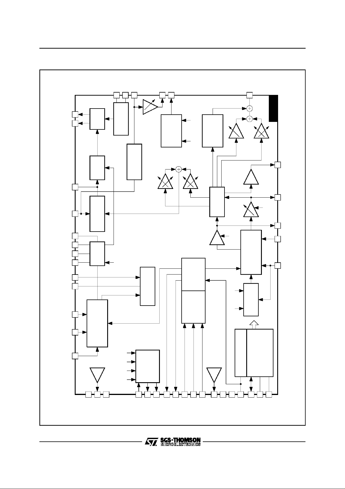
BLOCKDIAGRAM
HOUTEM
HOUTCOL
PLL2C
HFLY
FC2
FC1
C0
R0
HLOCKCAP
HLOCKOUT
20
21
8910
1112 1314
37
HOUT
BUFFER
PHASE
SHIFTER
PHASE
COMPARATOR
VCO
VCCX-RAY
HFOCUS
18
15
SAFETY
PROCESSOR
H-SAWTOOTH
2 bits
SafeFreq.
CAP
16
2
X
2 x 5 bits
Amp & Keyst
GENERATOR
Spin Bal
6 bits
HFOCUS
2 MOIRE
17
5 BITS
MOIRE
PROCESSOR
2
X
Key Bal
6 bits
CORNER
H-FLY VSYNC
X
SYNC
PROCESSOR
2
X
6 bits
(2 x 6 bits)
CORRECTION
TRACKING
GEOMETRY
7 bits
VPOS
EWOUT
31
X
7 bits
2
X
VERTICAL
OSCILLATOR
RAMP GENERATOR
TDA9106
7 bits
VAMP
32
25
27 28 29
OUT
CAP
V
DCOUT
AGCCAP
V
VFOCUS
V
V
4/30
HPOSFILTER
PLL1F
PLL1INHIB
PHASE/FREQUENCY
3 4
19
GND
COMPARATOR
H-PHASE(7 bits)
REF
V
567
HREF
HGND
LOCK
HFLY
VSYNC
VFLY
LOCK/UNLOCK
IDENTIFICATION
BLANKING
GENERATOR
30
22
233335
VFLY
VBLKOUT
HBLKOUT
1
36
S/G
HOUT
VSYNCOUT
SELECT
SYNC INPUT
38
H/HVIN
(2 bits)
VSYNCIN
V
26
V
REF
REF
24
VGND
6 bits 6 bits
RESET GENERATOR
34
39
5V
TEST
S AND C
CORRECTION
C INTERFACE
2
I
40
41
SCL
SDA
42
GND
9106A-02.EPS
TDA9106A
ABSOLUTE MAXIMUM RATINGS
Symbol Parameter Value Unit
V
V
V
VESD ESD susceptibility
T
T
THERMAL DATA
Symbol Parameter Value Unit
R
th (j-a)
Supply Voltage (Pin 18) 13.5 V
CC
Supply Voltage (Pin 39) 5.7 V
DD
Max Voltage on Pin6
IN
Pins 15, 21, 22, 23
Pin 1
Pin 4
Pins 3, 33,34,37,38,40,41
Pin 16
Pins 8, 9, 10, 11, 12, 13, 14, 25, 27, 30
1.8
12
3.6
4
5
6
8
2
Human Body Model,100pF Discharge through 1.5kΩ
EIAJ Norm,200pF Dischargethrough 0Ω
Storage Temperature -40, +150
stg
Junction Temperature +150
T
j
Operating Temperature 0, +70
oper
300
Junction-ambient Thermal Resistance Max. 65
kV
o
o
o
o
C/W
V
V
V
V
V
V
V
V
C
C
C
9106A-03.TBL
9106A-04.TBL
SYNCHROPROCESSOR
OperatingConditions
Symbol Parameter Test Conditions Min. Typ. Max. Unit
HsVR Horizontal Sync Input Voltage Pin 38 0 5 V
MinD Minimum Horizontal Input Pulses Duration Pin 38 0.7 µs
Mduty Maximum HorizontalInput Signal Duty Cycle Pin 38 25 %
VsVR Vertical Sync Input Voltage Pin 33 0 5 V
VSW Minimum Vertical Sync Pulse Width Pin 33 5 µs
VSmD Maximum Vertical Sync Input Duty Cycle Pin 33 15 %
VextM Maximum Vertical Sync Width on TTL
H/Vcomposite or S/G
ElectricalCharacteristics
(V
DD
=5V,T
amb
=25oC)
Symbol Parameter Test Conditions Min. Typ. Max. Unit
VSGDC S/G Clamped DC Level Pin 1, I
ISGbias Internal Diode Bias Current Pin 1, V
VSGTh SlicingLevel (see application design choice) Pin 1 0.2 V
VINTH Horizontal and Vertical Input Voltage
(Pins 33,38)
RIN Horizontaland Vertical Pull-Up Resistor Pins 33,38 200 kΩ
VOut Output Voltage (Pins 35,36,37) Low level
TfrOut Falling and Rising Output CMOS Buffer Pins 35,36,37
VHlock Horizontal 1st PLLLock Output Status (Pin 37) Locked
VoutT Extracted Vsync Integration Time (% of TH) on
H/V Composite or S/G
Pins 1, 38 750 µs
=-1µA1V
1
= 1.6V 10 µA
1
Low Level
0.8 V
High Level 2.2
0
High Level
5
100 ns
Cout = 20pF
0
Unlocked
5
Pin 35, C0 = 820pF 26 35 %
V
V
V
V
V
9106A-05.TBL
5/30
TDA9106A
I2C READ/WRITE
ElectricalCharacteristics
Symbol Parameter Test Conditions Min. Typ. Max. Unit
2
I
C PROCESSOR
Fscl Maximum Clock Frequency Pin 40 400 kHz
Tlow Low period of the SCL Clock Pin 40 1.3 µs
Thigh High period of the SCL Clock Pin 40 0.6 µs
Vinth SDA and SCL Input Threshold Pins 40,41 2.2 V
VACK AcknowledgeOutput Voltage onSDA inputwith3mA Pin 41 0.4 V
See also I2CTable Control and I2C Sub Address Control
HORIZONTAL SECTION
OperatingConditions
Symbol Parameter Test Conditions Min. Typ. Max. Unit
VCO
R
0(Min.)
C
0(Min.)
F
(Max.)
OUTPUT SECTION
I6m Maximum Input Peak Current Pin 6 2 mA
HOI1
HOI2
Minimum Oscillator Resistor Pin 11 6 kΩ
Minimum Oscillator Capacitor Pin 10 390 pF
Maximum Oscillator Frequency 150 kHz
Horizontal Drive Output Maximum Current
Pin 20
Pin 21
(V
DD
=5V,T
amb
=25oC)
Sourced current
Sunk current
2020mA
mA
ElectricalCharacteristics (VCC=12V,T
amb
=25oC)
Symbol Parameter Test Conditions Min. Typ. Max. Unit
SUPPLY AND REFERENCE VOLTAGES
V
V
I
I
V
REF-H
V
REF-V
I
REF-H
I
REF-V
Supply Voltage Pin 18 10.8 12 13.2 V
CC
Supply Voltage Pin 39 4.5 5 5.5 V
DD
Supply Current Pin 18 50 mA
CC
Supply Current Pin 39 5 mA
DD
Horizontal Reference Voltage Pin 5, I = 5mA 7.4 8 8.6 V
Vertical Reference Voltage Pin 5, I = 5mA 7.4 8 8.6 V
Max. SourcedCurrent on V
Max. SourcedCurrent on V
REF-H
REF-V
Pin 5 5 mA
Pin 26 5 mA
9106A-05.TBL
6/30

TDA9106A
HORIZONTAL SECTION (continued)
ElectricalCharacteristics
Symbol Parameter Test Conditions Min. Typ. Max. Unit
1st PLL SECTION
HpolT Polarity Integration Delay 0.75 ms
V
Vcog VCO Gain (Pin 12) R
Hph Horizontal Phase Adjustment % of Horizontal Period ±10 %
Hphmin
Hphtyp
Hphmax
dF0/dT FreeRunning Frequency Thermal Drift
CR PLL1 Capture Range R
PLLinh PLL1 Inhibition (Pin3) Typ Threshold = 1.6V
SFF Safe Forced Frequency
FC1
FC2
2nd PLL SECTION AND HORIZONTAL OUTPUT SECTION
FBth Flyback Input Threshold Voltage (Pin 6) 0.65 0.75 V
Hjit Horizontal Jitter (see Pins 8-9 filtering) TBD ppm
XRAYth X-RAY Protection Input Threshold Voltage Pin 15 8 V
Vphi2 Internal Clamping Levels on 2nd PLL Loop
VSCinh Threshold Voltage To Stop H-Out,V-Out
IHblk Maximum Horizontal Blanking Output
VHblk Horizontal Blanking Output Low Level
HDvd
HDem
Notes :
VCO Control Voltage (Pin12) V
VCO
Horizontal Phase Decoupling Output
Minimum Value
Typical Value
Maximum Value
Free Running Frequency R0= 6.49kΩ,C0= 820pF,
f
0
(No drift on external components)
SF1 Byte 11xxxxxx
SF2 Byte 10xxxxxx
VCO Sawtooth Level
High FC1=(4.V
Low FC2=(V
REF-H
Horizontal Drive Output Duty-Cycle
(Pin 20 or 21) (see Note 1)
Filter (Pin 4)
when V
< VSCinh
CC
Current
(Blanking ON)
Horizontal Drive Output
Low Level (Pin 20 to GND)
High Level (Pin 21 to V
1. Duty Cycle is the ratio of power transistorOFF time to period.Power transistor is OFF when output transistor is OFF.
2. Initial Condition for Safe Operation Start Up (Max. duty cycle).
(V
REF-H
)/5
CC
)/5
=12V,T
=12V)
CC
=25oC) (continued)
amb
REF-H
f
0
fH(Max.)
= 6.49kΩ,C0= 820pF,
0
dF/dV = 1/11R
Sub-Address 01, Pin 14
Byte x1111111
Byte x1000000
Byte x0000000
= 0.97/8R0C
f
0
= 6.49kΩ,C0= 820pF,
0
from f
fH(Min.)
f
H
PLL ON
PLL OFF 2
Sub-Address 02
Pin 9 To filter
Pin 8 To filter
Low Level
High Level
Pin 18 7.5 V
I
22
V
with I22= 10mA 0.25 0.5 V
22
V
21-V20,IOUT
V
20,IOUT
=8V
0C0
0
+0.5kHz to 4.5F
0
0
(Max.) 100
= 20mA
= 20mA 9.5
V
/6
REF-H
6.2
17 kHz/V
2.8
3.4
4.0
22.3 kHz
-150 ppm/C
23.5 kHz
0.8 V
2F0
3F0
6.4
1.6
48 %
1.6
4.0
10 mA
1.1
1.7 V
10
V
V
V
V
V
kHz
V
V
V
V
V
V
9106A-05.TBL
7/30
TDA9106A
HORIZONTAL SECTION (continued)
ElectricalCharacteristics
Symbol Parameter Test Conditions Min. Typ. Max. Unit
HORIZONTAL DYNAMIC FOCUS SECTION
HDFst Horizontal Dynamic Focus Sawtooth
HDFdis Horizontal Dynamic Focus Sawtooth
HDFDC Bottom DC Output Level R
TDHDF DC Output Voltage Thermal Drift 200 ppm/C
HDFamp Horizontal Dynamic Focus Amplitude
HDFKeyst Horizontal Dynamic Focus Keystone
MOIRE OUTPUT
R
MOIRE
V
MOIRE
Minimum Level
Maximum Level
Discharge Width
Min Byte xxx11111
Typ Byte xxx10000
Max Byte xxx00000
Min A/B Byte xxx11111
Typ Byte xxx10000
Max A/B Byte xxx00000
Minimum Output Resistor Pin 2 2 kΩ
Output Voltage (moire off),
Subaddress 0F
(V
CC
=12V,T
=25oC) (continued)
amb
HfocusCap = C
= 90kHz, Pin 16 2
f
H
Driven by Hfly 500 ns
= 10kΩ, Pin 17 2 V
LOAD
Sub-Address 03, Pin 17,
= 90kHz, Keystone Typ 1
f
H
Sub-Address 04,
= 90kHz, Typ Amp
f
H
B/A
A/B
A/B
Pin 2, R
Byte 0xx00000
Byte 0xx10000
Byte 0xx11111
MOIRE
= 820pF,
0
=2kΩ
4.7
1.5
3
3.5
1.0
3.5
0.2
1.1
2.0
V
V
V
PP
V
PP
V
PP
V
V
V
9106A-05.TBL
8/30
TDA9106A
VERTICALSECTION
OperatingConditions
Symbol Parameter Test Conditions Min. Typ. Max. Unit
OUTPUTS SECTION
VEWM Maximum EW OutputVoltage Pin 31 6.5 V
VEWm Minimum EW Output Voltage Pin 31 1.8 V
VDFm Minimum Vertical DynamicFocus Output Voltage Pin 32 1.8 V
R
LOAD
Minimum Load for less than 1% Vertical Amplitude Drift Pin 25 65 MΩ
ElectricalCharacteristics
(V
CC
=12V,T
amb
=25oC)
Symbol Parameter Test Conditions Min. Typ. Max. Unit
VERTICAL RAMP SECTION
VRB Voltage at Ramp BottomPoint V
VRT Voltage at Ramp Top Point (with Sync) V
REF-V
VRTF Voltage at Ramp Top Point (withoutSync) Pin 27 VRT-
=8V, Pin 27 2 V
REF-V
Pin 27 5 V
V
0.1
VSTD Vertical Sawtooth Discharge Time Duration
With 150nF Cap 80 µs
(Pin 27)
VFRF Vertical FreeRunning Frequency
(see Notes 3 & 4)
ASFR AUTO-SYNC Frequency C
RAFD Ramp Amplitude Drift Versus Frequency at
Maximum Vertical Amplitude
Rlin Ramp Linearity on Pin 27 (see Notes 3 & 4) 2.5 < V
C
OSC (Pin 27)
Measured on Pin27,
27
See Note 5
C
27
50Hz < f and f < 165Hz
= 150nF
= 150nF ±5%
= 150nF
and V27< 4.5V 0.5 %
27
100 Hz
50 165 Hz
200 TBD ppm/Hz
Vpos Vertical Position Adjustment Voltage (Pin28) Sub Address 06
I
VPOS
Max Current on Vertical Position Output Pin 28 ±2mA
VOR Vertical Output Voltage
(peak-to-peak on Pin 29)
Byte x0000000
Byte x1000000
Byte x1111111 3.65
Sub Address 05
Byte x0000000
Byte x1000000
Byte x1111111 3.5
3.2
3.5
3.8
2.25
3
3.75
3.3 V
V
V
2.5 V
V
V
VoutDC DC Voltage on Vertical Output See Note 6, Pin 29 3.5 V
VOI Vertical Output Maximum Current (Pin29) ±5mA
dVS Max Vertical S-Correction Amplitude
x0xxxxxx inhibits S-CORR
x1111111 gives max S-CORR
Ccorr Vertical C-Corr Amplitude
x0xxxxxx inhibits C-CORR
Subaddress 07
PP
PP
at T/4
at 3T/4
∆V/V
∆V/V
SubAddress 08
Byte x1000000
Byte x1100000
Byte x1111111
-4
+4
-3
0
3
%
%
%
%
%
VflyTh Vertical Flyback Threshold Pin 30 1 V
VflyInh Inhibition of Vertical Flyback Input See Note 7, Pin 30 7.5 V
Notes : 3. WithRegister 07 at Byte x0xxxxxx (VerticalS-Correction Control) thenthe S correction is inhibited, consequentlythesawtooth has
a linear shape.
4. With Register 08 at Byte x0xxxxxx (Vertical C - Correction Control) then the C correction is inhibited,consequently the sawtooth
has a linear shape.
5. It is the frequency range for which the VERTICAL OSCILLATOR will automaticallysynchronize, using a single capacitor value on
Pin 27 and with a constantramp amplitude.
OUTDC = (7/16).VREF-V. Typically 3.5V for Vertical reference voltage typical value (8V).
6. V
7. WhenPin30 ( V
discharge time.
) - 0.5V, Vflyinput is inhibited and vertical blanking on vertical blanking outputis replacedby vertical sawtooth
REF-V
9106A-05.TBL
9/30

TDA9106A
VERTICALSECTION(continued)
ElectricalCharacteristics
Symbol Parameter Test Conditions Min. Typ. Max. Unit
EAST/WEST FUNCTION
EW
TDEW
EWpara Parabola Amplitude with Vamp Max, V-Pos Typ,
EWtrack Parabola Amplitude Function of V-AMP Control
KeyAdj Keystone Adjustment Capability with Typ Vpos,
KeyTrack Intrinsic Keystone Function of V-POS Control
Corner
Max
Corner
BalMax
INTERNAL HORIZONTAL DYNAMIC PHASE CONTROL FUNCTION
SPBpara Side Pin Balance Parabola Amplitude (Figure 2)
SPBtrack Side Pin Balance Parabola Amplitude function of
ParAdj Parallelogram Adjustment Capability with Vamp
Partrack Intrinsic Parallelogram Function of Vpos Control
Notes :
DC Output Voltage with Typ Vpos,Keystone,
DC
Corner and Corner Balance Inhibited
DC Output Voltage Thermal Drift See Note8 100 ppm/C
DC
Keystone, Corner and Corner Balance Inhibited
(tracking between V-AMP and E/W) with Typ
Vpos, Keystone, Corner and Corner Balance
Inhibited, EW TypAmplitude
(see Note 9)
Corne r and Cor ner Ba lan ce Inhibited , EW
Inhibited and Vertical Amplitude Max
(see Note 9 and Figure 4)
(tracking between V-POS and EW) with Corner
and Corner Balance Inhibited,EW Max Amplitude
and Vertical Amplitude Max (see Note9)
A/B Ratio
B/A Ratio
Max Corner CorrectionAmplitude withVamp Max,
V-POS Typ, EWamp, Keystone and Corner
Balance Inhibited (see Note 9)
Max Corner Balance Correction Amplitude with
Vamp Max, V-POS Typ, EWamp, Keystone and
Corner Inhibited
Subaddress 0C (see Note9)
with Vamp Max, V-POS Typ and Parallelogram
Inhibited (see Notes 9 & 10)
Vamp Control (tracking between Vamp and SPB)
with SPB Max, V-POS Typ and Parallelogram
Inhibited (see Notes 9 & 10)
Max, V-POS Typ and SPB Inhibited
(see Notes 9, 10 & 11)
(tracking between V-Pos and DHPC) with Vamp
Max, SP B Max and Par allelogram Inhibited
(see Notes 9 & 10)
A/B Ratio
B/A Ratio
8. These parameters are not tested on each unit. They are measured duringour internal qualification
9. Refers to Notes 3 & 4 from last section.
10.TH is the Horizontal PLL Period Duration.
11.Figure 2 is representing effect of dynamic horizontal phase control.
(V
CC
=12V,T
=25oC) (continued)
amb
Pin 31, see Figure 1 2.5 V
Subaddress 09
Byte 1x111111
Byte 1x100000
Byte 1x000000
2.6
1.4
0
Subaddress 05
Byte 10000000
Byte 11000000
Byte 11111111
0.45
0.8
1.4
Subaddress 0A
Byte 10000000
Byte 11111111
1
1
Subaddress 06
Byte x0000000
Byte x1111111
0.5
0.5
Subaddress 0B
∆EWout at T/6, 5T/6
Byte x1111111
Byte x1000000
+0.2
-0.2
Byte 01111111
∆EWout at T/4
∆EWout at 3T/4
+0.2
-0.2
Byte 01000000
∆EWout at T/4
∆EWout at 3T/4
-0.2
+0.2
Subaddress 0D
Byte x1111111
Byte x1000000
1.4
-1.4
Subaddress 05
Byte 10000000
Byte 11000000
Byte 11111111
0.5
0.9
1.4
Subaddress 0E
Byte x1111111
Byte x1000000
1.4
-1.4
Subaddress 06
Byte x0000000
Byte x1111111
0.5
0.5
V
V
V
V
V
V
V
PP
V
PP
V
V
V
V
V
V
%TH
%TH
%TH
%TH
%TH
%TH
%TH
9106A-05.TBL
10/30

TDA9106A
VERTICALSECTION(continued)
ElectricalCharacteristics
Symbol Parameter Test Conditions Min. Typ. Max. Unit
VERTICAL DYNAMIC FOCUS FUNCTION
VDF
TDVDF
VDFAMP Parabola Amplitude Function of Vamp (tracking
VDFKEY Parabola Assymetry Function of VPos Control
Notes :
Figure1 :
DC Output Voltage with V-Pos Typ See Figure3 6 V
DC
DC Output Voltage Thermal Drift See Note12 100 ppm/C
DC
between Vamp and VDF)
with V-Pos Typ
(see Figure 3) (see Note 13)
(tracking between V-Pos and VDF) with Vamp
Max. (see Note 13)
12. Parameter not tested oneach unitbutmeasured duringour internal qualificationprocedure including batches coming from corners
of our process and also temperature characterization.
13. S and C correctionsare inhibited so theoutput sawtooth has a linear shape.
E/WOutput
(V
CC
=12V,T
=25oC) (continued)
amb
Figure2 :
Subaddress 05
Byte 10000000
Byte 11000000
Byte 11111111
Subaddress 06
Byte x0000000
Byte x1111111
DynamicHorizontalPhase Control
Output
0.9
1.6
2.5
0.5
0.5
V
V
V
9106A-05.TBL
A
EW
Figure3 :
A
EW
PARA
DC
VerticalDynamic Focus Function
VDF
DC
AMP
B
A
SPB
PARA
9106A-03.EPS
Figure 4 :
KeystoneEffect on E/W Output
B
DHPC
DC
9106A-04.EPS
(PCCInhibited)
BVDF
9106A-05.EPS
Keyadj
9106-06A.EPS
11/30

TDA9106A
TYPICALVERTICAL OUTPUT WAVEFORMS
Function
Sub
Address
Pin Byte Specification Picture Image
Vertical Size 05 29
Vertical
Position
DC
06 28
Control
Vertical
S
07 29
Linearity
10000000
11111111
x0000000
x1000000
x1111111
x0xxxxxx
Inhibited
x1111111
2.25V
3.75V
3.2V
3.5V
3.8V
∆V
V
PP
∆V
=4%
V
PP
12/30
Vertical
C
Linearity
08 29
x1000000
x1111111
V
PP
V
PP
∆V
∆V
V
V
∆V
∆V
PP
PP
=3%
=3%
9106A-06.TBL/ 9106A-07.EPS TO 9106A-13.EPS

GEOMETRYOUTPUT WAVEFORMS
Function
Sub
Address
Pin Byte Specification PictureImage
EWamp
Typ.
10000000
TDA9106A
3.75V
2.75V
Trapezoid
Control
Pin Cushion
Control
Parrallelogram
Control
Side Pin
Balance
Control
0A 31
09 31
0E Internal
0D Internal
11111111
Keystone
Inhibited
1x000000
1x111111
SPB
Inhibited
x1000000
x1111111
Parallelogram
Inhibited
X10000000
x1111111
2.5V
3.7V
3.7V
3.7V
3.7V
2.5V
3.75V
2.75V
2.5V
0V
2.5V
1.4% TH
1.4% TH
1.4% TH
1.4% TH
Vertical
Dynamic
Focus
32
6V
2.5V
9106A-07.TBL/ 9106A-14.EPSTO9106A-22.EPS
13/30

TDA9106A
GEOMETRYOUTPUT WAVEFORMS(continued)
Function
Corner Control 0B 31
Sub
Address
Pin Byte Specification PictureImage
EWamp
Typ.
x1111111
Corner
effect
without
Corner
Corner Balance
Control
Note :
The specification of output voltage is indicated on 3.75V
sawtooth output voltage.
0C 31
01000000
EWamp
Typ.
10000000
11111111
Corner
effect
Corner
effect
Corner
effect
vertical sawtooth output condition.The output voltage depends on vertical
PP
9106A-07.TBL/9106A-23.EPSTO 9106A-30.EPS
14/30

I2C BUSADDRESS TABLE
SubAddress Definition
Slave Address(8C) : Write Mode
D8 D7 D6 D5 D4 D3 D2 D1
0 x x x x 0 0 0 0 Horizontal Drive Selection
1 x x x x 0 0 0 1 Horizontal Position
2 x x x x 0 0 1 0 Safety Frequency
3 x x x x 0 0 1 1 Synchro Priority / Horizontal Focus Amplitude
4 x x x x 0 1 0 0 Refresh / Horizontal Focus Keystone
5 x x x x 0 1 0 1 Vertical Ramp Amplitude
6 x x x x 0 1 1 0 Vertical Position Adjustment
7 x x x x 0 1 1 1 S Correction
8 x x x x 1 0 0 0 C Correction
9 x x x x 1 0 0 1 E/W Amplitude
A x x x x 1 0 1 0 E/W Keystone
B x x x x 1 0 1 1 Cbow Corner
C x x x x 1 1 0 0 Spin Corner
D x x x x 1 1 0 1 Side Pin Balance
E x x x x 1 1 1 0 Parallelogram
F x x x x 1 1 1 1 Moire Control Amplitude
TDA9106A
Slave Address(8D) :
D8 D7 D6 D5 D4 D3 D2 D1
0 x x x x 0 0 0 0 Synchro and Polarity Detection
ReadMode
15/30

TDA9106A
I2C BUSADDRESS TABLE (continued)
Table:
WRITE MODE
READ MODE
[] initial value
00
01
02
03
04
05
06
07
08
09
0A
0B
0C
0D
0E
0F
00
RegisterMap
D8 D7 D6 D5 D4 D3 D2 D1
Blk Sel
1, Blk
[0]
Xray
1, reset
[0]
Safety Frequency
1, on
[0], off
Sync Priority Horizontal Focus Amplitude
0, Vextr
[1], Vin
Detect
Refresh
[0], off
Vramp
0, off
[1], on
EW Sel
0, off
[1]
EW Key
0, off
[1]
Test H
1, on
[0], off
Test V
1, on
[0], off
Moire
1, on
[0], off
Hlock
0, on
[1], no
HDrive
0, off
[1], on
[1] [0] [0] [0] [0] [0] [0]
1, F0 x 2
[0], F0x 3
0, S/G
[1], H/V
[1] [0] [0] [0] [0] [0] [0]
[1] [0] [0] [0] [0] [0] [0]
S Select
1, on
[0]
C Select
1, on
[0]
[1] [0] [0] [0] [0] [0] [0]
Cbow Sel
1, on
[0]
Spin Sel
1, on
[0]
SPB Sel
0, off
[1]
Parallelo
0, off
[1]
Vlock
0, on
[1], no
[1] [0] [0] [0] [0] [0]
[1] [0] [0] [0] [0] [0]
[1] [0] [0] [0] [0] [0]
[1] [0] [0] [0] [0] [0]
[1] [0] [0] [0] [0] [0]
[1] [0] [0] [0] [0] [0]
[1] [0] [0] [0] [0] [0]
Xray
1, on
[0], off
Horizontal Phase Adjustment
[1] [0] [0] [0] [0]
Horizontal Focus Keystone
[1] [0] [0] [0] [0]
Vertical Ramp Amplitude Adjustment
Vertical Position Adjustment
S Correction
C Correction
East/West Amplitude
East/West Keystone
Cbow Corner
Spin Corner
Side Pin Balance
Parallelogram
Moire Control
[0] [0] [0] [0] [0]
Polarity Detection Synchro Detection
H/V pol
[1], negative
V pol
[1], negative
Vext det
[0], no det
H det
[0], no det
V det
[0], no det
16/30

OPERATINGDESCRIPTION
I - GENERAL CONSIDERATIONS
I.1 - Power Supply
The typical values of the power supply voltages
and VDDarerespectively12V and 5V.Perfect
V
CC
operationisobtainedif V
andVDDaremaintened
CC
in thelimits : 10.8to 13.2V and 4.5 to5.5V.
In order to avoid erratic operation of the circuit
during transient phase of V
switchingoff,thevalueof V
outputsofthecircuitareinhibitedifV
switching on, or
CC
ismonitoredand the
CC
islessthan
CC
7.5V typically.
Inthe same manner,V
set-up is made until V
ismonitoredand internal
DD
reaches 4V (see I2C
DD
ControlTablefor power on reset).
Inordertohavea verygoodpowersupplyrejection,
the circuit is internallypowered by several internal
voltage references (the unique typical value of
which is 8V). Two of these voltage references are
externallyaccessible,one for the verticalpart and
onefor thehorizontalone. If needed,thesevoltage
references can be used (until load is less than
5mA).Furthermoreit is necessaryto filterthe a.m.
voltagereferencesbythe useof externalcapacitor
connectedtoground,inordertominimizethenoise
and consequently the “jitter” on vertical and horizontaloutput signals.
2
C Control
I.2 - I
TDA9106A belongs to the I
2
C controlled device
family, instead of being controlled by DC voltages
ondedicatedcontrolpins, each adjustmentcanbe
realizedthroughthe I
2
C bus is a serial bus with a clockand a data
TheI
2
C Interface.
input.Thegeneralfunctionandthebusprotocolare
specifiedin the Philips-bus data sheets.
The interface (Data and Clock) is TTL-level compatible. The internal threshold level of the input
comparatoris 2.2V (whenV
is 5V). Spikesof up
DD
to 50ns are filtered by an integratorand maximum
clockspeed is limited to 400kHz.
The data line (SDA) can be used in a bidirectional
way that means in read-mode the IC clocksout a
reply information(1 byte) to the micro-processor.
The bus protocol prescribes always a full-byte
transmission.Thefirst byte afterthestart condition
is used to transmit the IC-address(7 bits-8C) and
the read/writebit (0 write - 1 read).
TDA9106A
I.3 - WriteMode
In write mode the second byte sent contains the
subaddress of the selected function to adjust (or
controlstoaffect)andthethirdbytethe corresponding data byte.It is possible to send more than one
data byte to the IC. If after the thirdbyte no stop or
start condition is detected, the circuit increments
automatically the momentary subaddress in the
subaddress counter by one (auto-increment
mode).So it is possibletotransmitimmediatelythe
next data byteswithout sendingthe IC address or
subaddress.It canbe usefulso asto reinitializethe
whole controls very quickly (flash manner). This
procedurecan be finishedby a stop condition.
The circuit has 14 adjustment capabilities : 1 for
Horizontalpart,4 for Verticalone,2forE/Wcorrection, 2 for original Corner correction, 2 for the
Dynamic Horizontal phase control,1 for Moire option and 2 forHorizontalDynamicFocus.
20 bits are also dedicated to several controls
(ON/OFF, Horizontal Safety Frequency, Synchro
Priority, Detection Refresh and Xrayreset).
I.4 - Read Mode
During read mode the second byte transmits the
reply information.
The reply byte contains Horizontal and Vertical
Lock/Unlockstatus,Xray activatedor not,theHorizontal and Vertical polarity detection. It also contains Synchrodetection status that is useful forµP
to assignSync priority.
A stop condition always stops all activities of the
bus decoder and switches the data and the clock
line (SDAand SCL)to high impedance.
2
C Subaddressand control tables.
See I
I.5 - SynchroProcessor
TheinternalSync ProcessorallowstheTDA9106A
to acceptany kind of input synchro signals :
- separated Horizontal & Vertical TTL-compatible
sync signals,
- composite Horizontal &Vertical TTL-compatible
sync signals,
- sync on green or compositevideo signal.
17/30

TDA9106A
OPERATINGDESCRIPTION (continued)
I.6 - Sync IdentificationStatus
TDA9106Ais ableto feedbacktotheMCU (thanks
2
toI
C) the Syncinputstatus(syncidentification)so
thatthe MCUcan chooseSyncprioritythroughI
AsextractedVerticalsyncpulseis performedwhen
choicealreadyoccured andwhen 12Vis supplied,
werecommendto usethedeviceasfollowing:(that
means that even in Powermanagement mode the
IC is able to inform MCU on detected synchro
signalsdue to its 5V supply).
First,refreshSynchrodetection byI
the status of H/Vdet and Vdet by I
2
C.Then check
2
C read.
Syncpriority choice shouldbe :
Table1 : Sync PriorityChoice
Sync priority
H/V det V det
Yes Yes 1 1 Separated H & V
Yes No 0 1 Composite TTL
No No 0 0 Sync on Green
Subaddress 03
D8 D7 Synchro type
Comment
H&V
Of course, when choice is done, one can refresh
the synchro detections and verify that extracted
Vsyncis present and thatno synchro type change
occured.
Synchro processor is also giving synchro polarity
information.
I.7 - IC status
TheICcaninformtheMCUeitherthe1stHorizontal
PLLorVerticalsectionare lockedornot, andif Xray
hasbeen activated.
This last status permits to the MCU:
- reset the Xray internal latchdecreasing the V
supply
- directlyreset throw the I
2
C interface.
2
C.
CC
I.8 - SynchroInputs
Both H/HVin and Vsyncin inputs are TTLcompatibletriggerwith Hysterisistoavoiderraticdetection.
It includes pull up resistor to V
DD
.
Vertical sync extractor is included for composite
syncorcompositevideo.Applicationengineermust
adapt resistor R and capacitor C dedicatedto its
application.
Figure 5
1.6V
S/GRC 1kΩ
1
I
(Typ.)
REF
µA
=10
TDA9106
ResistorR isfixed by detectionthresholdwanted:
R<(V
THRESHOLD/IREF
)
Then C is determined by maximum pulse width to
detect(in general, vertical sync width) :
RC > (maxpulse width)
I.9 - SynchroProcessor Outputs
Synchro processor delivers on 3 TTL-compatible
CMOSoutputsthe following signals :
- Hout as follow :
Sync Mode Hout Mode Hout Polarity
Separated Horizontal Same as Input
TTL Composite TTL Composite Same as Input
S/G Composite Negative
- Vsyncoutis either vertical extracted pulseoutput
or Vsyncininput. It keeps the input polarity.
- HlockoutistheHorizontal1stPLLstatus:0Vwhen
locked. It permits MCU to adjust free running
frequencyand optimizesthe IC performance.
9106A-31.EPS
18/30

OPERATINGDESCRIPTION (continued)
II - HORIZONTAL PART
II.1 - Internal Input Conditions
Horizontalpart isinternally fed by synchroprocessorwithadigitalsignal.correspondingtohorizontal
synchropulses or to TTLcomposite input.
Concerning the duty cycle of the input signal, the
following signals (positive or negative) may be
appliedto the circuit.
Using internal integration,both signals are recognizedonconditionthat Z/T<25%.Synchronization
occurs on the leading edge of the internal sync
signal.The minimumvalue of Z is0.7µs.
Figure6
Another integrationisable to extractvertical pulse
ofcompositesynchroifdutycycleismorethan25%
(typicallyd = 35%).
Figure7
C
TDA9106A
designedin CMOStechnology.This kind of phase
detector avoids locking on false frequencies. It is
followed by a “charge pump”, composed of two
current sources sunk and sourced (I = 1mA Typ.
when locked, I = 140µA when unlocked). This
difference between lock/unlock permits a smooth
catching of horizontal frequency by PLL1. This
effectisreinforcedbyaninternaloriginalslowdown
system when PLL1 is locked avoiding Horizontal
too fast frequency change.
The dynamic behaviour of the PLL is fixed by an
external filter which integrates the current of the
chargepump.A“CRC”filteris generallyused (see
Figure 8).
PLL1is internallyinhibitedduringextractedvertical
sync (if any) to avoid taking in account missing
pulses or wrong pulses on phase comparator.The
inhibition results from the opening of a switch locatedbetween the charge pump and the filter(see
Figure 9). For particular synchro type, MCU can
drive Pin 3 to high level (TTLcompatible input) to
inhibit PLL1. It can also be used to avoid PLL1
lockingon synchro inputs if a “dangerous”mode is
9106A-32.EPS
detectedby the MCU.
TheVCOusesan externalRC network.It deliversa
linearsawtoothobtainedbychargeanddischargeof
the capacitor,by a currentproportionnalto the currentintheresistor.Typicalthresholdsofsawtoothare
1.6Vand6.4V.Thesetwolevelsareaccessibleto be
filteredas on Figure10 to improvejitter.
TRAMEXT
dd
The last featureperformed is the equalizing pulses
removingtoavoidparasiticpulsesonphasecomparatorinputwhichis intolerenttowrongormissingpulse.
II.2 - PLL1
The PLL1 is composed of a phase comparator,an
externalfilterandavoltagecontr ol l edoscilla tor(VC O).
Thephase comparatoris a “phasefrequency”type
Figure 8
9106A-33.EPS
PLL1F
12
9106A-34.EPS
19/30

TDA9106A
OPERATINGDESCRIPTION (continued)
Figure9 : PLL1 BlockDiagram
H-LOCKCAP
13
S/G
1
VSYNCIN
H/HVIN
Figure10 :
Loop
Filter
(1.3V < V < 6V)
33
38
* SMFE : Safety Frequency Mode Enable
SYNC
PROCESSOR
TRAMEXT
Detailsof VCO
I
0
12
12
11
R0
The control voltage of the VCO is typically comprisedbetween1.33Vand6V(seeFigure 10).The
theoricalfrequencyrange of thisVCOis intheratio
1 to 4.5, the effective frequency range has to be
smaller1 to 4.2 due to clamp interventionon filter
lowestvalue.
The synchro frequency has to be always higher
thanthe freerunningfrequency.As an examplefor
a synchrorange from 24kHz to 100kHz, the suggestedfree running frequency is 23kHz.
An other feature is the capability for MCU to force
horizontal frequencythrough I
2
C to 2xF0 or 3xF0
(for burn in mode or safety requirement).In this
case,inhibitionswitch is openedleavingPLL1free
butvoltageonPLL1filterisforcedto 2.66Vfor2xF0
or 4.0V for 3xF0.
The PLL1 ensures the coincidence between the
leading edge of the synchro signal and a phase
reference obtained by comparison between the
sawtooth of the VCO and an internal DC voltage
2
C adjustable between 2.8V and 4.0V (corre-
I
sponding to ± 10%) (see Figure 11). This voltage
hasto be filtered on Pin14 so as to optimize jitter.
20/30
4
I
0
2
I
0
LOCKDET
COMP1
E2
10
C0
High
Low
6.4V
1.6V
6.4V
1.6V
LOCK/UNLOCK
STATUS
CHARGE
PUMP
0 0.875T T
PLL1INHIB
TRAMEXT SMFE *
INHIBITION
H-POS
PHASE
ADJUST
RS
FLIP FLOP
3
PLL
14
PLL1F R0 C0
12 11 10
VCO
OSC
I2C
HPOS
Adj.
9
47nF 47nF
8
The TDA9106A also includes a Lock/Unlockidentification block which sensesin real time wheither
PLL1 is locked on the incoming horizontal sync
signalor not. The resultinginformation is available
on Hlockout (see Synchro Processor). The block
Figure 11 : PLL1TimingDiagram
H Osc
Sawtooth
7/8T
H
Phase REF1
H Synchro
Phase REF1is obtainedbycomparison between thesawtoothand
a DC voltage adjustable between 2.8V and 4.0V. The PLL1 ensures the exact coincidencebetween thesignals phase REF and
HSYNS. A ± T/10 phase adjustment is possible.
1/8T
H
6.4V
2.8V<Vb<4.0V
Vb
1.6V
9106A-35.EPS
9106A-36.EPS
9106A-37.EPS

OPERATINGDESCRIPTION (continued)
Figure12 : LOCK/UNLOCKBlock Diagram
From
Phase
Comparator
A
NOR1
20kΩ
220nF
H-Lock CAP
functionis describedin Figure 12.
TheNOR1 gate is receiving the phasecomparator
output pulses (which also drive the chargepump).
When PLL1 is locked, on point A there is a very
small negative pulse (about 100ns) at each horizontalcycle, so after RC filter,there is a high level
on Pin 13 which forces Hlockout to low level. Hysterisis comparator detects locking when Pin 13 is
reaching 6.5V and unlocking when Pin 13 is decreasingto 6.0V.
WhenPLL1 is unlocked, the 100ns negative pulse
on A becomes much larger and consequently the
averagelevelon Pin 13 decreases.It forcesHlockout to go high.
ThePin 13 status is approximatelythe following:
- near 0V when there is no H-Sync
- between 0 and 4V with H-Sync frequencydifferent from VCO
- between 4 to 8 V when VCO frequency reaches
H-Sync one (but not already in phase)
- near 8V when PLL1 is locked.
Figure13 :
PLL2 TimingDiagram
H Osc
Sawtooth
Flyback
Internally
Shaped
H Drive
Flyback
Ts
Duty Cycle48%
7/8T
1/8T
H
H
6.4V
4.0V
1.6V
TDA9106A
5V
HLOCKOUT
37
6V
B
HFLY
400Ω
6
20kΩ
GND 0V
Q1
13
6.5V
It is important to notice that Pin 13 is not an
output pin but is only used for filtering purpose
(see Figure 12).
Thelock/unlockinformationis also availablethrow
2
I
C read.
II.3 - PLL2
Figure 14 : Flyback Input ElectricalDiagram
The PLL2 ensures a constant position of the
shaped flyback signal in comparionwith the sawtoothof the VCO(Figure 13).
The phase comparator of PLL2 (phase type comparator)isfollowedbya chargepumpwith ± 0.5mA
(typ.)outputcurrent.
The flybackinput is composed of an NPN transistor. This input must be current driven. The maximum recommanded input current is 2mA
(see Figure 14).
The duty cycle is fixed and equal to 48% of horizontal-period.
Maximumstoragetimeisabout43.75%-(Tfly/2.TH).
Ty pi c ally,Tfly/T Hisaround20%thatmeansTsmaxis
around33.75%.
II.4 - OutputSection
The H-drive signal is transmitted to the output
througha shapingblockensuringTsanddutycycle.
In order to secure scanningpower part operation,
the output is inhibited in the following circum-
9106A-39.EPS
stances:
9106A-38.EPS
9106A-40.EPS
21/30

TDA9106A
OPERATINGDESCRIPTION (continued)
Figure16 : Output stage simplified diagram,
showingthe two possibilitiesof
connection
V
21
CC
20
V
CC
21
20
-V
too low
CC
- Xrayprotectionactivated
- During horizontalflyback
2
C bit control (voluntary inhibition by MCU).
-I
Theoutputstageis composedof aNPN Darlington
H-DRIVE
H-DRIVE
bipolartransistor.
Both the collector and the emittor are accessible
(seeFigure 16).
TheoutputDarlingtonisinoff-statewhenthepower
scanningtransistor is also inoff-state.
The maximum output current is 20mA, and the
correspondingvoltagedropoftheoutputdarlington
is 1.1V typically.
It is evident that the power scanning transistor
cannot be directly driven by the integrated circuit.
Aninterfacehas tobedesignedbetweenthecircuit
andthe power transistorwhichcanbe of bipolar or
MOStype.
II.5 - X-RAYProtection
The activation of the X-Ray protectionis obtained
by application of a high level on the X-Ray input
(Pin15 > 8V).The consequenciesof X-Rayprotectionare :
9106A-41.EPS
- inhibitionof H-Drive output
- activationof horizontal blanking output.
- activationof vertical blankingoutput.
The reset of this protection is obtained either by
V
switchoff orI2C resetby MCU(see Figure17).
CC
Figure17 : SafetyFunctions Block Diagram
VCCChecking
V
CC
Ref
XRAYProtection
XRAY
VCCoffor I2C Reset
HorizontalFlyback
0.7V
I2C SFME
HorizontalFree Running Detection
VerticalFree Running Status
HorizontalUnlock
VerticalFlyback
VerticalSync
Vertical Sawtooth Retrace
Vertical Unlock
I2C Rampon/off
S
Q
R
LOGIC
BLOCK
I2C Drive on/off
HORIZONTAL
OUTPUT
INHIBITION
I2C Ramp on/off
VERTICAL
OUTPUT
INHIBITION
I2C Blanking
HORIZONTAL
BLANKING
OUTPUT
VERTICAL
BLANKING
OUTPUT
9106A-42.EPS
22/30

OPERATINGDESCRIPTION (continued)
Figure18
Horizontal Flyback
Internal Trigged
Horizontal Flyback
Horizontal Focus
Cap Sawtooth
Horizontal Dynamic
Focus Parabola
Output
Moire Output
II.6 - Horizontal Dynamic Focus
TDA9106A delivers an horizontal parabola wave
formon Pin 17. This parabola is performed from a
sawtoothin phasewithflybackpulse.Thissawtooth
is present on Pin 16 where the horizontal focus
capacitoris the same as C0 to obtain a controlled
amplitude(from 2 to 4.7V typically).
Symmetry(keystone)andamplitudeareI
2
Cadjustable (see Figure 18).This signal has to be connected to the CRT focusing grids and mixed with
verticaldynamic focus.
Figure19 :
Moire Function Block Diagram
TDA9106A
4.7V
2V
400ns
2V
9106A-43.EPS
II.7 - Moire Output
The moire output is intented to correct a beat
between horizontal video pixel period and actual
CRTpixel width.
Themoiresignalis a combinationofHorizontaland
Verticalfrequencysignals.
To achieve a moire cancellation,it has to be connected to any point on the chassiscontrolling the
horizontalposition.Werecommendtointroducethis
Figure20 :
H-FLY
V-SYNC
Moire OutputWaveform
EVEN FRAME
H
V
MOIRE
ODD FRAME
H
V
Monostable
Ck
D
Ck
D
Rst
Q
Q
Q
Q
23
9106A-44.EPS
MOIRE
9106A-45.EPS
23/30

TDA9106A
OPERATINGDESCRIPTION
“HorizontalControlledJitter”on the relativegroundofPLL2capacitorwhere this“controlledjitter”frequency
type will directlyaffect the horizontalposition.The amplitudeof the signal is I
One point to noticeis :
- in case H-Moire is not necessary in the applica-
tion, H-Moire output (Pin 2) can beturnedtoas a
5 bits digital to analog converter output (0.3V to
2.2V V output voltage),
- in case of no use in application,this pin mustbe
left high impedance(orresistor to ground).
(continued)
2
C adjustable.
(keystoneadjustment).
Corner and Corner Balance corrections may be
added to the E/W one. Theseare respectively3rd
and 2nd order waveforms.
In order to keep a good screen geometry for any
end user preferencesadjustmentwe implemented
the “geometry tracking”.
Due to large output stages voltage range (E/W,
III - VERTICAL PART
III.1- Geometric Corrections
Theprinciple is representedin Figure21.
Startingfrom the verticalramp, a parabolashaped
current is generated for E/W correction, dynamic
horizontal phase control correction, and vertical
dynamicFocus correction.
The base of the parabola generator is an analog
multiplierthe output current ofwhichis equalto :
2
∆I=k⋅(V
OUT-VDCOUT
)
Where Vout is the vertical output ramp, typically
comprisedbetween2 and 5V,Vdcoutisthe vertical
DC output adjustablein the range 3.2V ≥ 3.8V in
orderto generatea dissymetricparabolaifrequired
Figure21 :
GeometricCorrections Principle
FOCUS),the combinationof trackingfunctionwith
maximum vertical amplitude max or min vertical
position and maximum gain on the DAC control
mayleadto theoutputstagessaturation.Thismust
be avoided by limiting theoutput voltage by apropriate I
2
C registersvalues.
ForE/WpartandDynamicHorizontalphasecontrol
part, a sawtooth shaped differential current in the
followingform is generated:
∆
I’= k’⋅(V
OUT-VDCOUT
2
)
Then∆I and∆I’ are addedtogetherand converted
into voltage for the E/W part.
Each of the four E/W componentsor the two DynamicHorizontalphasecontrolonesmay beinhibited by theirown I
2
C select bit.
VDCOUT
VerticalRampV
VerticalRamp V
VMID
2
32
OUT
EWamp
VDCIN
Keystone
31
OSC
Corner
VDCOUT
CornerBalance
Sidepinamp
VDCOUT
Parallelogram
To Horizontal
Phase
VerticalDynamic
FocusOutput
EWOutput
SidepinBalance
OutputCurrent
9106A-46.EPS
24/30

OPERATINGDESCRIPTION (continued)
TheE/WparabolaisavailableonPin31 bythe way
ofan emitterfollowerwhich has tobe biasedby an
externalresistor(10kΩ). It canbe DC coupledwith
externalcircuitry.
Theoutput connectionof the vertical DynamicFocusis the same as the E/W one.
This reverse parabola is availableon Pin32.
Dynamic Horizontal phase control current drives
internally the H-position,moving the Hfly position
onthe Horizontalsawtooth in the range± 2.8% Th
bothon SidePinBalance and Parallelogram.
TDA9106A
typically3.5V
K1 is adjustableby EW amplitude I
K2 is adjustableby Keystone I
K3 is adjustableby Cbow Corner I
K4 is adjustableby Spin Corner I
III.3 - DynamicHorizontal Phase Control
I
OUT
=K5(V
OUT-VDCOUT
)2+K6(V
K5 is adjustableby SidePin Balance I
K6 is adjustableby Parallelogram I
2
C register
2
C register
2
C register
2
C register
OUT-VDCOUT
2
2
C register
C register
)
III.2- EW
EWOUT= 2.5V+ K1 (V
+K2(V
+K3(V
+K4(V
is theramp Pin 27and V
V
OSC
Figure22 :
VSYNCIN
H/HVIN
VerticalPart Block Diagram
1
S/G
33
38
OUT-VDCOUT
OUT-VDCOUT
OUT-VDCOUT
SYNC
PROCESSOR
POLARITY
OUT-VDCOUT
)
)2|V
)|V
OSC-VMID
the middle of it,
MID
OSCILLATOR
2
)
OSC-VMID
DISCH.
Corner
SUB0B/6bits
CORNER
|
|
27
OSC
CAP
Corner Balance
SUB0C/6bits
III.4 - VerticalDynamic Focus
VFOC
=6V - 0.7 (V
OUT
OUT-VDCOUT
2
)
No adjustment is available for this part except by
meansof tracking.
III.5 - VerticalSawtoothGenerator
TRANSCONDUCTANCE
AMPLIFIERCHARGECURRENT
REF
25
Sawth.
Disch.
SAMP.
CAP
VERT_AMP
SUB05/7bits
S CORRECTION
VS_AMP
SUB07/6bits
COR_C
SUB08/6bits
C CORRECTION
29
VERT_OUT
SAMPLING
Vlow
PARABOLA
GENERATOR
EW_CENT
SUB0A/6bits
PARAL
SUB0E/6bits
EW_AMP
SUB09/6bits
SPB_AMP
SUB0D/6bits
31
EW_OUT
SPB_OUT
32
V_FOCUS
Internal Signal to PLL2
9106A-47.EPS
25/30

TDA9106A
OPERATINGDESCRIPTION (continued)
Thevertical partgeneratesa fixed amplitude ramp
whichcanbeaffectedbySandCcorrectionshape.
Then,theamplitudeof thisrampisadjustedto drive
an externalpower stage (see Figure 22).
Theinternal referencevoltage used forthe vertical
part is available between Pin 26 and Pin 24. Its
typicalvalue is :
V
26=VREF
The charge of the external capacitor on Pin 27
(VCAP)generatesafixedamplituderampbetween
theinternalvoltages,V
5/8 x V
REF
).
Whenthe synchronizationpulse isnot present,an
internal current source sets the free running frequency.For an externalcapacitor, C
the typical freerunning frequencyis 106Hz.
Typical free running frequency can be calculated
by :
(Hz) =
f
0
A negative or positive TTL level pulse applied on
Pin33 (VSYNC)as well as a TTL composite sync
on Pin 38 or a Sync on Green signal on Pin 1 can
synchronise the ramp in the range [fmin , fmax].
This frequency range depends on the external
capacitor connected on Pin 27. A capacitor in the
range [150nF, 220nF] ± 5% is recommanded for
applicationin the followingrange : 50Hzto120Hz.
Typicalmaximumand minimumfrequency,at25
and without any correction (S correction or C correction),can be calculatedby :
= 2.5 x f0and f
f
(Max.)
If S or C corrections are applied, these values are
slightyaffected.
If a synchronization pulse is applied, the internal
oscillatoris automaticalysynchronizedbutthe amplitudeis no more constant.An internalcorrection
isactivatedto adjustit in less than a half a second
: the highest point of theramp (Pin 27) is sampled
on the sampling capacitor connected on Pin 25 at
eachclockpulse and a transconductanceamplifier
generatesthe charge current of the capacitor.The
ramp amplitude becomes again constant and frequencyindependant.
Theread status register enables to have the vertical Lock-Unlock and the vertical Sync Polarity in-
=8V
l(Vl=VREF
−5
1.6 e
⋅
(Min.)
/4) andVH(VH=
= 150nF,
OSC
1
C
OSC
= 0.33 x f
0
o
C
formations.
It is recommandedto usea AGCcapacitorwithlow
leakagecurrent.A value lower than100nAis mandatory.
Goodstabilityof theinternalclosed loopisreached
bya470nF± 5%capacitorvalueon Pin25 (VAGC).
Pin 30, VFLYis the vertical flyback input used to
generate the vertical blanking signal on Pin 23. If
Vfly is not used, (V
- 0.5),atminimum, must be
REF
connectedto this input.
In such case, the vertical blanking output will be
activated by the vertical sync input signal and resetted by the end of vertical sawtooth discharging
pulse.
2
III.6 - I
C Control Adjustments
Then, S and C correction shapes can be added to
this ramp. This frequency independent S and C
corrections are generated internally. Their amplitudeareadjustableby theirrespectiveI
2
C register.
They can also be inhibitedby their Selectbit.
At the end, the amplitudeof thisSand C corrected
ramp can be adjusted by the vertical ramp amplitude control register.
The adjustedramp is available onPin 29 (V
OUT
)to
drive an external power stage.
The gain of this stage is typically 25%depending
on its register value.
The DC value of this ramp is kept constant in the
frequency range, for any correction applied on it.
its typical value is V
A DC voltage is available on Pin 28 (VDCOUT). It
is driven by its own I
Its value is V
So theV
of V
OUT
DCOUT
voltageis correlatedwith DCvalue
DCOUT
. It increases the accuracy when tempera-
= 7/16 ⋅ V
MID
2
C register (vertical Position).
= 7/16⋅V
REF
.
REF
±
300mV.
ture varies.
III.7 - Basic Equations
In firstapproximation,theamplitudeof the rampon
Pin 29 (Vout)is :
V
OUT-VMID
with V
MID
=(V
= 7/16 ⋅ V
OSC-VMID
REF
) ⋅ (1 + 0.25 (V
; typically3.5V,the middle
AMP
))
value of theramp on Pin 27
V
OSC=V27
V
AMP
, rampwith fixedamplitude
is -1 for minimum vertical amplitude register
26/30

APPLICATION DIAGRAMS
Figure23 : DemonstrationBoard
+12V
PC2
47kΩ
ICC1 - MC14528
CC4
TA1
1
47pF
TA2
2
+12V
CDA
3
IA
4
IA
5
QA
6
QA
7
GND QB
89
R35
10kΩ
J8
1
HFLY
TP14
XRAYIN
J7
1
DYNAMIC
FOCUS
J9
1
3.9kΩ
HBLK
TP2
TP8
VBLK
R45
33kΩ
R45
33kΩ
R25
1kΩ
R21
33pF
16
V
CC
CC3
15
TB1
47pF
14
TB2
+12V
13
CDB
12
IB
11
IB
QB
10
R10
C25
10kΩ
33pF
C22
R8
10kΩ
R7
10kΩ
V_FOCUS
R24
10kΩ
+12V
R27
3.9kΩ
10µF
J10
CC2
47kΩ
R48
1kΩ
100nF
+12V
PC1
JP1
C33
6.49kΩ
100µF
TP9
R20
10Ω
TP15
C21
47nF
R23
1%
C31
4.7µF
C5
CC1
100nF
+12V
C26
R22
1µF
1.5kΩ
R44
10kΩ
C7
22nF
HREF
C27
47µF
C16
220pF
C23
47nF
C28
820pF
5%
C13 10nF
R36 1.8kΩ
C17 220nF
C29 1µF
C34 820pF
C6
100nF
IC2
C44
TDA9106
10pF
SYNC/G GNDD
1
MOIRE SDA
2
3
PLL2C +5V
4
5
6
HFLY HLOCKOUT
HGND HOUT
7
8
FC1
9
C0
10
R0 V_FOCUS
11
PLL1F
12
13
HLOCKCAP
HPOS
14
XRAYIN
15
H_FOCUSC VCAP
16
17
V
18
CC
19
20
HOUTEM
HOUTCOL
21
1J16
+5V
H/HVINHREF
VSYNCOUTFC2
TEST
VSYNCIN
EWOUT
VFLY
VOUT
VDCOUT
VREFH_FOCUS
VAGCCAP
VGNDGND
V_BLKOUT
H_BLKOUT
TDA9106A
432
1
J141J15
+5V
R39
R29
4.7k
4.7k
Ω
42
41
SCLPLLINH
40
39
C30
100µF
TP1
J11
HSYNC
38
TP17
37
TP10
TP11
36
TP12
35
34
J12
VSYNC
TP17
33
TP16
V_FOCUS
32
R28 10kΩ
31
30
29
28
TP5
C12
27
150nF
26
25
24
23
22
C15
470nF
100nF
C2
C39
22pF
R42
100
Ω
Ω
R41
100Ω
L1 10µH
C32
100nF
VREF
VREF
C3
47µF
10µF
C40
R49
22pF
22kΩ
+5V
D2
1N4148
R32
4.7kΩ
R16
15kΩ
R40
12kΩ
R1
12kΩ
VERTICAL
DEFLECTION
STAGE
L3 10µH
+12V
HORIZONTAL
DRIVER
STAGE
C45
IC3 - STV9422
24
PWM7
23
PWM6
22
TEST
21
B
20
G
+5V
19
R
18
GND
17
RST
16
SDA
15
SCL
14
PWM5
13
PWM4
R30
10k
Ω
+12V
C36
1µF
R34
1kΩ
R33
4.7kΩ
E/W POWER STAGE
C4
R2
5.6kΩ
100nF
C41
470pF
C20
1µF
R13
1kΩ
C35
100nF
PWM0
1
PWM1
2
3
FBLK
L2 10µH
4
VSYNC
5
HSYNC
PXCK
CKOUT
XTALOUT
XTALIN
PWM2
PWM3
R37
27kΩ
R9
470Ω
7
TDA8172
1
R5
5.6kΩ
Q5
BC547
Q4
BC557 C24
V
BC557
2
IC1
-12V
DD
R15
1kΩ
Q2Q1
D1
1N4004
6
4
R6
10Ω
10
11
12
6
7
8
9
27kΩ
3
470µF
R31
5N20
270kΩ
39kΩ
5
C10
100µF
STD
8MHz
R17
R18
470µF
C18
100µF
36V
C19
63V
R14
22kΩ
C43
47µF
X1
C14
Q6
R43
10kΩ
33pF
33pF
R3
1.5Ω
C1
220nF
C8
100nF
T1
G5676-00
+5V
C7
C7
R19
270kΩ
C11
220pF
R12
560Ω
1nF
C9
100nF
TP8
TP7
2.2Ω 1W
Q3
TIP122
R47
82Ω 3W
HDRIVE
TP3 TP4
C42
1µF
R38
+12V
-12V 1
R11
220Ω
1/2W
R4
1Ω
1/2W
+24V
J13
1
TILT
J1
1
E/W
J2
1
J3
J18
1
2
3
V YOKE
J17
J6
1
2
3
1
9106A-48.EPS
27/30

TDA9106A
APPLICATION DIAGRAMS(continued)
Figure24 : PCB Layout
28/30
9106A-49.EPS

APPLICATION DIAGRAMS(continued)
Figure25 : ComponentsLayout
TDA9106A
29/30
9106A-50.EPS

TDA9106A
PACKAGEMECHANICALDATA
42 PINS - PLASTICSHRINK DIP
A2
A1
E
E1
LA
42
1
Dimensions
BeB1
D
22
21
c
SDIP42
Millimeters Inches
Min. Typ. Max. Min. Typ. Max.
e1
e2
E
.015
0,38
Gage Plane
e3
e2
A 5.08 0.200
A1 0.51 0.020
A2 3.05 3.81 4.57 0.120 0.150 0.180
B 0.38 0.46 0.56 0.0149 0.0181 0.0220
B1 0.89 1.02 1.14 0.035 0.040 0.045
c 0.23 0.25 0.38 0.0090 0.0098 0.0150
D 36.58 36.83 37.08 1.440 1.450 1.460
E 15.24 16.00 0.60 0.629
E1 12.70 13.72 14.48 0.50 0.540 0.570
e 1.778 0.070
e1 15.24 0.60
e2 18.54 0.730
e3 1.52 0.060
L 2.54 3.30 3.56 0.10 0.130 0.140
Informationfurnishedis believed to be accurateand reliable.However, SGS-THOMSONMicroelectronics assumesno responsibility
for theconsequences of use of such information nor for any infringement of patentsor other rights of third parties which may result
from itsuse. No licence is granted by implication orotherwise underany patent or patent rightsof SGS-THOMSON Microelectronics.
Specifications mentioned in this publication are subject to change without notice. This pu blication supersedes and replaces all
informationpreviouslysupplied.SGS-THOMSON Microelectronics products arenotauthorized for use as criticalcomponents in life
support devices or systemswithout express written approval of SGS-THOMSON Microelectronics.
PMSDIP42.EPS
SDIP42.TBL
30/30
1997 SGS-THOMSON Microelectronics - All Rights Reserved
Purchase of I2C Components of SGS-THOMSON Microelectronics, conveys a license under the Philips
2
C Patent. Rights to use these components in a I2C system,is granted provided that the system conforms to
I
2
the I
C StandardSpecifications as defined by Philips.
SGS-THOMSON Microelectronics GROUP OF COMPANIES
Australia - Brazil- Canada- China- France - Germany - Italy - Japan - Korea - Malaysia - Malta - Morocco
The Netherlands - Singapore- Spain - Sweden - Switzerland - Taiwan - Thailand - UnitedKingdom - U.S.A.
 Loading...