


TDA9105A
DEFLECTIONPROCESSOR FOR MULTISYNC MONITORS
PRODUCT PREVIEW
HORIZONTAL
.
DUALPLLCONCEPT
.
150kHzMAXIMUM FREQUENCY
.
SELF-ADAPTATIVE
.
X-RAYPROTECTIONINPUT
.
DC ADJUSTABLEDUTY-CYCLE
.
1stPLLLOCK /UNLOCK INFORMATION
.
WIDE RANGE DC CONTROLLED H-POSITION
.
ON/OFF SWITCH (FOR PWR MANAGEMENT)
.
TWOH-DRIVE POLARITIES
VERTICAL
.
VERTICALRAMP GENERATOR
.
50 TO185Hz AGC LOOP
.
DCCONTR OLLE DV-A MP,V-PO S,S-AMP& C-COR
.
ON/OFFSWITCH
EWPCC
.
VERTICAL PARABOLA GENERATOR WITH
DCCONTROLLEDKEYSTONE& AMPLITUDE
.
AUTOTRACKINGWITH V-POS& V-AMP
.
CORNER CORRECTION WITH DC CONTROLLEDAMPLITUDE
GEOMETRY
.
WAVE FORM GENERATOR FOR PARALELLOGRAM& SIDE PIN BALANCECONTROL
.
AUTOTRACKINGWITH V-POS& V-AMP
DYNAMICFOCUS
.
VERTICALPARABOLAOUTPUTFOR VERTICALDYNAMICFOCUS
.
AUTOTRACKINGWITH V-POS& V-AMP
GENERAL
.
ACCEPT POSITIVE OR NEGATIVE HORIZONTAL& VERTICALSYNC POLARITIES
.
SEPARATEH & V TTL INPUT
.
COMPOSITEBLANKINGOUTPUT
DESCRIPTION
The TDA9105A is a monolithic integrated circuit
assembled in a 42 pins shrink dual in line plastic
package.
This IC controls all the functions related to the
horizontaland verticaldeflection in multimodesor
multisyncmonitors.
This IC, combined with TDA9205 (RGB preamp),
STV942x(OSDprocessor),ST727x(micro controller)and TDA817x(verticalbooster),allowsto realize very simple and high quality multimodes or
multisyncmonitors.
SHRINK42
(Plastic Package)
ORDER CODE : TDA9105A
PIN CONNECTIONS
V-FOCUS
H-LOCKOUT
PLL2C
H-DUTY
H-FLY
H-GND
H-REF
FC2
FC1
C0
R0
PLL1F
H-LOCKCAP
PLL1INHIB
H-POS
XRAY-IN
H-SYNC
V
GND
H-OUTEM
H-OUTCOL
1
2
3
4
5
6
7
8
9
10
11
12
13
14
15
16
17
18
CC
19
20
21
42
41
40
39
38
37
36
35
34
33
32
31
30
29
28
27
26
25
24
23
22
SPINBAL
KEYBAL
GEOMOUT
EWAMP
KEYST
EWOUT
V-FLY
VDCIN
V-SYNC
V-POS
VDCOUT
V-AMP
V-OUT
C-CORR
VS-AMP
V-CAP
V-REF
V-AGCCAP
V-GND
CORNER
BLK-OUT
9105A-01.EPS
July 1997
Thisis advanceinformation on a new product now in developmentor undergoingevaluation . Details are subject to changewithout notice.
1/31

TDA9105A
PIN DESCRIPTION
Pin Name Function
1 V-FOCUS Vertical Dynamic Focus Output
2 H-LOCKOUT First PLL Lock/Unlock Output
3 PLL2C Second PLL Loop Filter
4 H-DUTY DC Controlof HorizontalDriveOutput PulseDuty-cycle.If thisPin isgrounded, theHorizontal
5 H-FLY Horizontal Flyback Input (positive polarity)
6 H-GND Horizontal Section Ground
7 H-REF Horizontal Section Reference Voltage, must be filtered
8 FC2 VCO Low Threshold Filtering Capacitor
9 FC1 VCO High Threshold Filtering Capacitor
10 C0 Horizontal Oscillator Capacitor
11 R0 Horizontal Oscillator Resistor
12 PLL1F First PLL Loop Filter
13 H-LOCKCAP First PLL Lock/Unlock Time Constant Capacitor. When Frequency is changing, a Blanking
14 PLL1INHIB TTL-Compatible Input for PLL1 OutputCurrent Inhibition
15 H-POS DC Control for Horizontal Centering
16 XRAY-IN X-RAY protection Input (with internal latch function)
17 H-SYNC TTL compatible Horizontal Sync Input
18 V
CC
19 GND Ground
20 H-OUTEM Horizontal Drive Output (emiter of internal transistor)
21 H-OUTCOL Horizontal Drive Output (open collector of internal transistor)
22 BLK OUT BlankingOutput, activated during frequency changes, when X-RAY Input is triggered,when
23 CORNER DC Control of Corner Correction Amplitude
24 V-GND Vertical Section Signal Ground
25 V-AGCCAP Memory Capacitor for Automatic Gain Control Loop in Vertical Ramp Generator
26 V-REF Vertical Section Reference Voltage
27 V-CAP Vertical Sawtooth Generator Capacitor
28 VS-AMP DC Control of Vertical S-Shape Amplitude
29 C-CORR DC Control of Vertical C-Correction
30 V-OUT Vertical Ramp Output (with frequency independant amplitude and S-Correction)
31 V-AMP DC Control of Vertical Amplitude Adjustment
32 VDCOUT Vertical Position Reference Voltage Output
33 V-POS DC Control of Vertical Position Adjustment
34 V-SYNC TTL-Compatible Vertical Sync Input
35 VDCIN Geometric Correction Reference Voltage Input
36 V-FLY Vertical Flyback Input (positive polarity)
37 EWOUT East /West Pincushion Correction Parabola Output
38 KEYST DC Control of Keystone Correction
39 EWAMP DC Control East/West Pincushion Correction Amplitude
40 GEOMOUT Side Pin Balance & Parallelogram Correction Parabola Output
41 KEYBAL DC Control of Parallelogram Correction
42 SPINBAL DC Control of Side Pin Correction Amplitude
and VerticalOutputs are inhibited. By connectinga Capacitor on this Pin a Soft-startfunction
may be realized on H-drive Output.
Pulse is generated on Pin 23, the durationof this Pulse is proportionnal to the Capacitor on
Pin 13.
Supply Voltage (12V Typ.)
VS istoolow, or when Device is instand-bymode(through H-DUTYPin 2)andduringH-FLY,
V-FLY, V-SYNC, VSawth retrace.
9105A-01.TBL
2/31
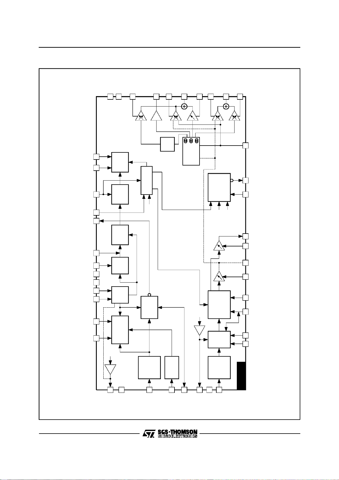
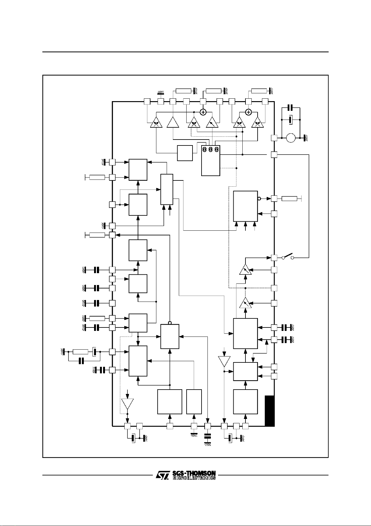
BLOCKDIAGRAM
GND18V
19
TDA9105A
CC
CORNER
23
V-FOCUS
1
38
KEYST
EWOUT
37
EWAMP
39
KEYBAL
41
GEOMOUT
SPINBAL
40
42
H-OUTEM
20
H-OUTCOL
21
H-DUTY
4
XRAY-IN
16
H-LOCKOUT
2
PLL2C
3
H-FLY
5
FC1
9
FC2
8
R0
11
C0
10
PLL1F
12
H
BUFFER
OUTPUT
PULSE
SHAPER
PHASE
SHIFTER
COMP
PHASE
VCO
SAFETY
PROCESSOR
VS
VIDEO UNLOCK
LOCK
IDENT
UNLOCK
2
X
2
X
BLK
GEN
H-FLY
V-SYNC
VDCIN
35
22
36
32
33
30
31
BLK-OUT
V-FLY
VDCOUT
V-POS
V-OUT
V-AMP
V-MID
VAGCCAP
VCAP
RAMP
VERT OSC
GENERATOR
25
27
V-REF
H-POS
COMP
15
PHASE
FREQUENCY
S
CORR
29
28
C-CORR
VS-AMP
V-REF
7
H-REF
6
H-GND
POL
PULSE
SHAPER
17
H-SYNC
DETECT
PLL1
INHIB
14
PLL1INHIB
13
26
V-REF
H-LOCKCAP
PULSE
24
V-GND
POL
DETECT
SHAPER
34
V-SYNC
TDA9105A
9105A-02.EPS
3/31
TDA9105A
QUICK REFERENCEDATA
Parameter Value Unit
Horizontal Frequency 15 to 150 kHz
Autosynch Frequency (for Given R0, C0) 1 to 3.7 FH
Hor Sync Polarity Input YES
±
Compatibility with Composite Sync on H-SYNC Input YES (see note 1)
Lock/Unlock Identification on 1
DC Control for H-Position YES
X-RAY Protection YES
Hor DUTY Adjust YES
Stand-by Function YES
Two Polarities H-Drive Outputs YES
Supply Voltage Monitoring YES
PLL1 Inhibition Input YES
Composite Blanking Output YES
Horizontal Moire Output NO
Vertical Frequency 35 to 200 Hz
Vertical Autosync (for 150nF) 50 to 185 Hz
Vertical S-Correction YES
Vertical C-Correction YES
Vertical Amplitude Adjustment YES
Vertical Position Adjustment YES
East/West Parabola Output YES
PCC (Pin Cushion Correction) Amplitude Adjustment YES
Keystone Adjustment YES
Corner Correction Adjustment YES
Dynamic Horizontal Phase Control Output YES
Side Pin Balance Amplitude Adjustment YES
Parallelogram Adjustment YES
Tracking of Geometric Corrections with V-AMP and V-POS YES
Reference Voltage YES (see note 2)
Mode Detection NO
Vertical Dynamic Focus YES
Notes : 1. Provided PLL inhibitioninput is used, seeapplication diagram on page 27.
2. One for Horizontal section and one for Verticalsection.
st
PLL YES
9105A-02.TBL
4/31

TDA9105A
ABSOLUTEMAXIMUM RATINGS
Symbol Parameter Value Unit
V
CC
V
IN
VESD ESD Succeptibility
T
stg
T
T
oper
THERMAL DATA
Symbol Parameter Value Unit
R
th (j-a)
HORIZONTAL SECTION
OperatingConditions
Symbol Parameter Test Conditions Min. Typ. Max. Unit
VCO
R0min Oscillator Resistor Min Value(Pin 11) 6 kΩ
C0min Oscillator Capacitor Min Value (Pin 10) 390 pF
Fmax Maximum Oscillator Frequency 150 kHz
HsVR Horizontal Sync Input Voltage(Pin 17) 0 5.5 V
INPUT SECTION
MinD MinimumInput Pulses Duration (Pin 17) 0.7 µS
Mduty Maximum Input Signal Duty Cycle(Pin 17) 25 %
OUTPUT SECTION
I5m Maximum Input Peak Current (Pin 5) 5 mA
HOI1
HOI2
DC CONTROL VOLTAGES
DCadj DC Voltage on DC Controls (Pins 4-15) V
Supply Voltage (Pin 18) 13.5 V
Max Voltage on Pins 4, 15, 28, 29, 31, 33, 38, 39, 41, 42
Pin 5
Pins 17, 34
Pin 16, 2, 22
Pin 14
Human Body Model, 100pF Discharge through 1.5kΩ
EIAJ Norm, 200pF Discharge through 0Ω
8
1.8
6
12
5
2
300
Storage Temperature -40, +150 °C
Max Operating Junction Temperature 150 °C
j
Operating Temperature 0, +70 °C
Junction-Ambient Thermal Resistance Max. 65 °C/W
Horizontal Drive Output Max Current
Pin 20
Pin 21
Sourced current
Sink current
=8V 2 6 V
REF-H
20
20
V
V
V
V
V
kV
V
9105A-03.TBL
9105A-04.TBL
mA
mA
9105A-05.TBL
5/31
TDA9105A
HORIZONTAL SECTION (continued)
(V
ElectricalCharacteristics
= 12V,T
CC
Symbol Parameter Test Conditions Min. Typ. Max. Unit
SUPPLY AND REFERENCE VOLTAGES
V
V
I
REF-H
V
I
REF-V
Supply Voltage (Pin 18) 10.8 12 13.2 V
CC
Supply Current (Pin 18) See Figure 1 45 65 mA
I
CC
Reference Voltage for Horizontal Section (Pin 7) I = 2mA 7.4 8 8.6 V
REF-H
Max Sourced Current on V
Reference Voltage for Vertical Section (Pin 26) I = 2mA 7.4 8 8.6 V
REF-V
Max Sourced Current on V
(Pin 7) 5 mA
REF-H
(Pin 26) 5 mA
REF-V
INPUT SECTION/PLL1
V
V
V
Horizontal Input Threshold Voltage (Pin 17) Low level voltage
INTH
VCO Control Voltage (Pin 12) V
VCO
VCO Gain, dF/dV (Pin12) R0 = 6.49kΩ, C0 = 680pF 17 kHz/V
COG
Hph Horizontal Phase Adjust (Pin 15) % of Horizontal period
f0 FreeRunning Frequency (adjustable by changing R0) R0 = 6.49kΩ, C0 = 680pF 25 27 29 kHz
CR PLL1 Capture Range
PLLinh PLL 1 Inhibition (Pin 14) PLL ON
(Typ. Threshold = 1.6V) PLL OFF
I
HLock0
V
HLock0
Max Output Current on HLock Output I
Low Level Voltage on HLock Output V2with I2= 10mA 0.25 0.5 V
SECOND PLL ANDHORIZONTALOUTPUT SECTION
FBth Flyback Input Threshold Voltage (Pin 5) See Figure 14 0.60 0.70 V
Hjit Horizontal Jitter See ApplicationDiagram
Horizontal Drive Output Duty-cycle
(Pin 20 or 21) (see Note)
HDmin
HDmax
Minimum
Maximum
HDvd Horizontal Drive Low Level Output Voltage Pin 20 to GND,
HDem Horizontal Drive High Level Output Voltage
(output on Pin 20)
XRAYth X-RAYProtectionInput Threshold Voltage(Pin16) TBD 8 TBD V
ISblkO Maximum Output Current on Composite Blanking
Output
VSblkO Low-Level Voltageon Composite Blanking Output
(Blanking ON)
Vphi2 Internal Clamping Voltage on 2nd PLL Loop Filter
Output (Pin 3)
V
Threshold Voltage to Stop H-out, V-out and to
OFF
activate BLKout (OFF mode when V
(Pin 4)
VSCinh Supply Voltage to Stop H-out , V-out when
< VSCinh (Pin18)
V
CC
Note : If H-drive is taken on Pin 20 (Pin 21 connected to supply), H-D is the ratio of low level durationto horizontal period.
If H-drive is taken on Pin 21 (Pin 20 grounded), H-D is the ratio of high level duration to horizontal period.
Inboth cases, H-D period driving horizontal scanning transistor off.
amb
Fh Min
Fh Max
=25°C)
4<VOFF
High level voltage 2
= 8V 1.6 to 6.2 V
REF-H
12.5 %
±
R0 = 6.49kΩ, C0 = 680pF
See conditions on Fig. 1
f0
3.7 x f0
V
14
V
14
2
2
80 ppm
(Pins 8-9)
=2V
V
4
=6V
V
4
V
4=VREF
- 500mV
31
54.5
33.2
57
61.5
1.1 1.7 V
V
21-V20,IOUT
Pin 21 to V
= 20mA
I
OUT
I
22
V
with I22= 10mA 0.25 0.5 V
22
Vmin
Vmax
V
4
)
= 20mA
,
CC
9.5 10 V
1.6
4.0
TBD 7.5 V
0.8 V
0.8 V
10 mA
35.5
59.5%%
10 mA
1V
kHz
kHz
V
%
V
V
9105A-06.TBL
6/31
TDA9105A
VERTICALSECTION
OperatingConditions
Symbol Parameter Min. Typ. Max. Unit
VSVR Vertical Sync Input Voltage (Pin 34) 0 5.5 V
VEWM Maximum EW Output Voltage (Pin 37) 6.5 V
VDHPCM Maximum Dynamic Horizontal Phase Control Output Voltage (Pin 40) 6.5 V
VDHPCm Minimum Dynamic Horizontal Phase Control OutputVoltage (Pin 40) 0.9 V
VDFm Minimum Vertical Dynamic Focus Output Voltage (Pin 1) 0.9 V
Rload Minimum Load for less than 1% Vertical Amplitude Drift (Pin 25) 65 M
Ω
9105A-07.TBL
Electrical Characteristics
(V
= 12V,T
CC
amb
=25°C)
Symbol Parameter Test Conditions Min. Typ. Max. Unit
I
BIASP
I
BIASN
VSth Vertical Sync Input Threshold Voltage (Pin 34) High-level
VSBI Vertical Sync Input Bias Current
V
V
V
BiasCurrent(currentsourcedbyPNPBase)(Pin28) For V28=2V 2 µA
Bias Current(Pins 29-31) (sinkedby NPN base) For V31= 6V, V29= 6V 0.5 µA
2
Low-level
= 0.8V 1 µA
V
(Current Sourced by PNP Base)
Voltage at Ramp Bottom Point (Pin 27) 2/8 V
RB
Voltageat RampTopPoint (with Sync) (Pin 27) 5/8 V
RT
Voltage at Ramp Top Point (without Sync)
RTF
(Pin 27)
34
VRT-0.1 V
0.8
V
V
REF-V
REF-V
VSW Minimum Vertical Sync Pulse Width (Pin 34) 5 µS
VSmDut Vertical Sync Input Maximum Duty-cycle
15 %
(Pin 34)
VSTD Vertical Sawtooth Discharge Time Duration
With 150nF cap 70
S
µ
(Pin 27)
VFRF Vertical Free RunningFrequency V
= 2V, V29grounded,
28
Measured on Pin 27
100 Hz
Cosc (Pin27) = 150nF
ASFR AUTO-SYNC Frequency (see Note 1) With C
RAFD Ramp AmplitudeDrift Versus Frequency V
50Hz < f < 185Hz
Rlin Ramp Linearity on Pin 30 V
Vpos Vertical Position Adjustment Voltage(Pin 32) V
V
V
I
VPOS
V
Max Current on Vertical Position Control Output
(Pin 32)
Vertical Output Voltage (Pin 30)
OR
(peak-to-peak voltage on Pin 30)
V31=2V
V
V
V
OUTDC
DC Voltage on Vertical Output (Pin30) See Note 2 7/16 V
V0I Vertical Output Maximum Current (Pin 30)
= 150nF 50 185 Hz
27
= 6V, C27= 150nF
31
grounded 0.5 %
28,V29
=2V
33
=4V
33
= 6V 3.65
33
100 ppm/Hz
3.2
3.5
3.8
±2mA
2
=4V
31
= 6V 3.75
31
3
4
5mA
±
3.3 V
V
V
2.2 V
V
V
REF-V
dVS Max Vertical S-Correction Amplitude
= 2V inhibits S-CORR
V
28
= 6V gives maximum S-CORR
V
28
Ccorr Max Vertical C-Correction Amplitude V
∆V/V
V/V
∆
V
V
at T/4
30pp
at 3T/4 TBD
30pp
=2V
29
=4V
29
= 6V TBD
29
-4
+4
-1.6
0
1.6
TBD %
%
TBD %
%
%
VFly Th Vertical Flyback Threshold (Pin 36) 1 TBD V
VFly Inh Inhibition of Vertical Flyback Input (Pin 36) See Note 1 V
I
BIAS DCIN
Notes : 1. It is thefrequency range for which the VERTICAL OSCILLATOR will automatically synchronize, using a single capacitor value on
Bias Current (Pin 35) (sourced by PNP base) For V35=V
Pin 27 and with a constant ramp amplitude.
2. Typically 3.5Vfor Vertical reference voltage typical value (8V).
32
- 0.5 V
REF
2
A
µ
9105A-08.TBL
7/31
TDA9105A
VERTICALSECTION(continued)
East/WestFunction
Symbol Parameter Test conditions Min. Typ. Max. Unit
EW
TDEW
EW
EW
Keytrack Keystone versus V-POS control
KeyAmp Keystone Amplitude Adjustment V
Notes : 1. When Pin36 > V
DC Output Voltage (see Figure 2) V33= 4V, V35=V32,
DC
DC Output Voltage Thermal Drift See Note 2 100 ppm/°C
DC
Parabola Amplitude V28= 2V, V29grounded,
para
Parabola Amplitude versus V-AMP
track
Control (tracking between V-AMP
and E/W)
(tracking between V-POS and EW)
A/B Ratio
B/A Ratio
-0.5V,Vflyinput isinhibited and verticalblankingon composite blankingoutput is replaced byvertical sawtooth
discharge time.
2. These parameters are not tested on each unit. They are measured during our internal qualification procedure which includes
characterization on batches comming from corners of our processes and also temperature characterization.
REF
= 4V, V23=4V
V
38
= 6V, V33= 4V,
V
31
V
35=V32,V38
V
39
V
39
= 2V, V29grounded
V
28
= 4V, V35=V
V
33
V38= 4V, V39= 6V, V23=4V
V
31
V
31
V
31
= 4V, V28= 2V, V29grounded,
V
23
= 6V, V38= 4V, V39=6V
V
31
= 2V, V35=V
V
33
V33= 6V, V35=V
= 4V, V31= 6V, V39=2V
23
V
38
V
38
V
38
= 4V, V23=4V
=6V
=2V
32
=2V
=4V
=6V
32
32
=4V
=2V
=6V
TBD 1.70
2.5 V
0
0.45
1.0
1.7
0.54
0.54
0
1.3
1.3
V
V
V
V
V
V
V
V
9105A-09.TBL
DynamicHorizontalPhase Control Function
Symbol Parameter TestConditions Min. Typ. Max. Unit
DHPC
TDDHPC
SPBpara SidePinBalance ParabolaAmplitude
SPBtrack Side Pinbalance Parabola Amplitude
ParAdj Parallelogram Adjustment Capability
Partrack Parallelogram versus V-posControl
DC Ouput Voltage (see Figure 3) V33= 4V, V35=V32,V41=4V 4 V
DC
DC Output Voltage ThermalDrift See Note 100 ppm/°C
DC
= 2V, V29grounded,
V
28
= 6V, V33= 4V,
(see Figure 3)
ve r sus V-amp C ontrol (tra c k ing
between V-amp and SPB )
A/B ratio (see Figure.3)
B/A ratio
(tracking between V-pos and DHPC)
A/B ratio
B/A ratio
V
31
V
35=V32,V41
V
42
V
42
= 2V, V29grounded,
V
28
= 4V, V35=V32,
V
33
= 4V, V42=6V
V
41
V
31
V
31
V
31
= 2V, V29grounded,
V
28
= 6V, V33= 4V,
V
31
V
35=V32,V42
V
41
V
41
= 2V, V29grounded,
V
28
= 6V, V41= 4V, V42=6V
V
31
= 2V, V35=V32,
V
33
= 6V, V35=V
V
33
=4V
=6V
=2V
=2V
=4V
=6V
=6V
=6V
=2V
32
TBD +1.45
- 1.45 TBD
0.36
0.82
1.45
TBD
TBD
0.12
0.12
0.53
0.53
V
V
V
V
V
9105A-10.TBL
8/31

TDA9105A
VERTICALSECTION(continued)
VerticalDynamic Focus Function
Symbol Parameter Test Conditions Min. Typ. Max. Unit
VDF
TDVDF
VDFAMP Parabola Amplitude versus V-amp
VDFKEY Parabola Assymetry versus V-pos
Corner
Amplitude
DC Output Voltage (see Figure 4) V33= 4V, V35=V
DC
DC Output Voltage ThermalDrift See Note 100 ppm/C
DC
= 2V, V29grounded,
V
28
= 4V, V35=V32,
(tracking between V-amp and VDF)
(see Figure 4)
Control (tracking between V-pos
and VDF)
A/B ratio
B/A ratio
Corner Amplitude Adjustment V
V
33
=2V
V
31
=4V
V
31
=6V
V
31
= 2V, V29grounded,
V
28
= 6V,
V
31
V
= 2V, V35=V32,
33
= 6V, V35=V
V
33
= 4V, V38= 4V, V39=2V
31
=2V
V
23
=4V
V
23
=6V
V
23
32
-0.84
-1.78
-3.14
0.42
32
0.42
Tracking Corner with V-amp V23=6V
=2V
V
31
=4V
V
31
=6V
V
31
Note : These parameters are not tested on each unit. They are measured during our internal qualification procedure which includes
characterization on batches comming from corners of our processes and also temperature characterization.
6V
-0.72
-1.57
-2.85
0.54
0.54
0.55
0.55
0.2
0.55
1.7
-0.6
-1.36
-2.56
V
V
V
0.64
0.64
V
PP
0
V
PP
V
PP
VPP
V
PP
V
PP
9105A-11.TBL
9/31
TDA9105A
Figure1 : TestingCircuit
1kΩ
CC
V
Ω
CORNER
23
10k
1
19
38
10kΩ
10kΩ
100nF
40
37
41
39
42
2.2µF
CC12V
18
V
2
X
2
X
35
H
BUFFER
21 20
OUTPUT
V
CC
1.8kΩ
10nF
SAFETY
416
PULSE
SHAPER
PROCESSOR
BLK
GEN
10kΩ
CC
V
36 22
VS
2
10kΩ
PHASE
22nF
47nF
47nF
53
SHIFTER
COMP
PHASE
6.49kΩ 0.1%
VIDEOUNLOCK
10 11 8 9
680pF 1%
4.7µF
15 12
1µF
VCO
COMP
PHASE
FREQUENCY
LOCK
IDENT
UNLOCK
V-MID
V-REF
H-FLY
V-SYNC
RAMP
VERT OSC
GENERATOR
S
CORR
470nF
1%
27 25 31 30 33 32
1%
150nF
28
10/31
7
V-REF
6
2.2µF
POL
PULSE
SHAPER
17
DETECT
PLL1
INHIB
14
13
220nF
262924
2.2µF
POL
PULSE
SHAPER
34
DETECT
TDA9105A
9105A-03.EPS

TDA9105A
Figure2 : ExampleofVertic alPositionTrackingEffect
EW
A
EW
DC
PARA
B
Figure4 : Corner Effecton E/W Output
V23=6V
=2V
V
23
Figure6 : Dynamic Horizontal Phase Control
Output
Figure3 : KeystoneEffect on E/W Output
9105A-04.EPS
Figure5 : E/WOutput with or withoutCorner
with corner
amplitude
V23>4V
9105A-06.EPS
Figure 7 : VerticalDynamicFocus Function
V38=6V
=2V
V
38
without
corner
with corner
amplitude
V23<4V
9105A-05.EPS
9105A-07.EPS
V
=6V
42
V41=6V
B
A
SPB
PARA
=2V
V
42
DHPC
DC
9105A-08.EPS
A
VDF
DC
AMP
BVDF
V33=2V
9105A-09.EPS
11/31

TDA9105A
TYPICALVERTICAL OUTPUT WAVEFORMS
Function
Control
Pin
Output
Pin
Control
Voltage
Specification Picture Image
Vertical Size 31 30
Vertical
Position
DC
33 32
Control
Vertical
DC
In/Out
35
37
40
Vertical
S
25 30
Linearity
2V
6V
2V
4V
6V
3.2V
3.5V
3.8V
2V
4V
This terminal is a Pin
1
controlling the center position
of geometric correction
signals. When connected to
Pin 32, “Autotracking” occurs.
2V
∆V
12/31
Vertical
C
Linearity
29 30
6V
2V
6V
V
PP
V
PP
V
PP
∆V
∆V
∆V
V
∆V
V
∆V
V
PP
PP
PP
=4%
= 1.6%
= 1.6%
9105A-13.TBL/ 9105A-10.EPS TO9105A-16.EPS

TYPICALGEOMETRY OUTPUT WAVEFORMS
Function
Control
Pin
Output
Pin
Control
Voltage
=4V
V
38
TDA9105A
Specification Picture Image
Trapezoid
Control
Pin Cushion
Control
Parrallelogram
Control
Side Pin
Balance
Control
38 37
39 37
41 40
42 40
2V
6V
=4V
V
39
2V
1.3V
2.5V
1.3V
0V
1.7V
6V
=4V
V
42
2V
6V
=4V
V
41
2V
4V
3V4V
3V4V
1.45V
1.45V
6V
Vertical
Dynamic
1
Focus
Corner 23 37
Note : The specification of Output voltage is indicated on 4VPPvertical sawtooth output condition.The output voltage depends on vertical
sawtooth output voltage.
6V
3V
1.7V
2.5V
13/31
9105A-14.TBL / 9105A-17.EPS TO 9105A-27.EPS

TDA9105A
OPERATINGDESCRIPTION
GENERAL CONSIDERATIONS
PowerSupply
The typical value of the power supply voltage V
is12V.Perfectoperationisobtainedif VCCismaintainedin thelimits : 10.8V→ 13.2V.
In order to avoid erratic operation of the circuit
duringthe transient phase of V
switchingoff, the valueof V
CC
outputsof the circuit are inhibited if V
switchingon, or
CC
ismonitoredand the
< 7.6typi-
CC
cally.
Inordertohavea verygoodpowersupplyrejection,
the circuit is internallypowered by several internal
voltage references (The unique typical value of
which is 8V). Two of these voltage referencesare
externallyaccessible,one for the vertical part and
one for the horizontal part. These voltage references can be used for the DC control voltages
appliedon theconcernedpinsby thewayof potentiometers or digital to analog converters (DAC’s).
Furthermoreit isnecessarytofilterthea.m. voltage
references by the use of external capacitor connected to ground, in order to minimize the noise
and consequently the “jitter” on vertical and horizontaloutput signals.
DCControl Adjustments
Thecircuit has 10 adjustmentcapabilities: 2 for the
horizontal part, 2 for the E/W correction, 4 for the
vertical part, 2 for the Dynamic Horizontal phase
control.
The correspondinginputs of the circuit has to be
driven with a DC voltage typically comprised between 2 and 6V for a value of the internal voltage
referenceof 8V.
CC
In order to have a good tracking with the voltage
reference value, it’s better to maintain the control
voltagesbetweenV
/4 and 3/4⋅V
REF
REF
.
The input currentof the DC control inputs is typically verylow (abouta fewµA). Dependingon the
internalstructureof the inputs, it canbe positive or
negative(sink or source).
HORIZONTAL PART
Inputsection
The horizontalinput is designed to be sensitiveto
TTLsignals typicallycomprised between0 and5V.
Thetypicalthresholdofthisinputis 1.6V.Thisinput
stageuses an NPNdifferentialstageand the input
currentis very low.
Figure 9 : Input Structure
H-SYNC 1.6V
Concerning the duty cycle of the input signal, the
followingsignals may be appliedto the circuit.
Using internal integration, both signals are recognizedon conditionthat Z/T≤25%.Synchronisation
occurs on the leading edge of the internal sync
signal. The minimum value of Z is 0.7µs.
Figure 10
9105A-29.EPS
Figure8 : Example of Practical DC Control
VoltageGeneration
V
REF
DC Control
PWM
DAC
Output
14/31
Voltage
PLL1
ThePLL1 is composedof a phasecomparator,an
external filter and a Voltage Controlled Oscillator
(VCO).
Thephasecomparatorisa “phasefrequency”type,
designedin CMOS technology.This kind of phase
detector avoids locking on false frequencies. It is
followed by a “charge pump”, composed of 2 cur-
9105A-28.EPS
rentsources sink and source (I = 1mAtyp.)
9105A-30.EPS

TDA9105A
OPERATINGDESCRIPTION
(continued)
Figure11 : Principle Diagram
13
LOCKDET
COMP1
E2
H-LOCKOUT
2
H-SYNC
H-LOCKCAP
17
INPUT
INTERFACE
The dynamic behaviour of the PLL is fixed by an
external filter which integrates the current of the
chargepump.A “CRC”filter is generally used(see
Figure9).
PLL1 is inhibitedby appl ying a high level on Pin 14
(PLLinhi b)whichisa TTLcompatibl einput.Theinhibition results from the openingof a switch locatedbetweenthechargepumpandthefilter(see Figure 8).
TheVCO uses an externalRC network.It delivers
a linear sawtooth obtained by charge and dischargeof the capacitor,by a currentproportionnal
to the current in the resistor. typical thresholds of
sawtoothare 1.6V and 6.4V (see Figure10).
The control voltage of the VCO is typically comprisedbetween 1.6V and 6V (see Figure 10). The
theoreticalfrequencyrangeofthisVCOisintheratio
1 → 3.75, but due to spread and thermal drift of
externalcomponentsandthecircuititself,theeffec-
Figure13 : Details of VCO
High
Low
CHARGE
PUMP
PLL1INHIB
INHIBITION
H-POS
PHASE
ADJUST
14
PLL
15
PLL1F R0 C0
12 11 10
VCO
OSC
3.2V
tive frequencyrangehas to be smaller(e.g. 30kHz
→ 85kHz).In theabsenceof synchronisationsignal
thecontrolvoltageisequalto1.6Vtyp.andtheVCO
oscillates on its lowest frequency(freefrequency).
Thesynchrofrequencyhastobealwayshigherthan
thefreefrequencyanda marginhas to be taken.As
an example for a synchro range from 30kHz to
85kHz,the suggestedfree frequencyis 27kHz.
Figure 12
PLL1F
12
9105A-31.EPS
9105A-32.EPS
Loop
12
Filter
(1.6V < V < 6V)
12
11
R0
I
0
2
I
0
4I
0
2
C0
10
6.4V
1.6V
6.4V
1.6V
0 0.75T T
RS
FLIP FLOP
9105A-33.EPS
15/31

TDA9105A
OPERATINGDESCRIPTION
(continued)
The PLL1 ensures the coincidence between the
leading edge of the synchro signal and a phase
reference obtained by comparison between the
sawtooth of the VCO and an internal DC voltage
adjustablebetween 2.4V and 4V (by Pin 15). So a
±45°phaseadjustmentis possible(see Figure11).
Figure14 : PLL1 TimingDiagram
H Osc
Sawtooth
Phase REF1
H Synchro
Phase REF1is obtainedby comparisonbetweenthe sawtoothand
a DC voltage adjustablebetween 2.4Vand 4V. The PLL1ensures
the exact coincidence between the signals phase REF and
HSYNS. A ± T/8 phase adjustment is possible.
0.75T 0.25T
6.4V
2.4V<Vb<4V
Vb
1.6V
Thetwo VCOthreshold can be filteredby connecting capacitoron Pins 8-9.
The TDA9103 also includes a LOCK/UNLOCK
identification block which senses in real-time
whetherthePLLis lockedon theincominghorizontal sync signal or not. The resulting information is
availableonHLOCKOUToutput (Pin2). The block
diagram of the LOCK/UNLOCK function is describedin Figure 12.
TheNOR1 gate is receivingthephase comparator
output pulses (which also drive the charge pump).
Whenthe PLL is locked, on pointA there is a very
small negative pulse (100ns) at each horizontal
cycle, so after R-C filter, there is a high level on
Pin13 which force HLOCKOUTto high level (provided that HLOCKOUTis pulledup toV
CC
When the PLL is unlocked, the 100ns negative
pulseonAbecomesmuchlargerandconsequently
the average level on Pin 13 will decrease. When it
reaches 6.5V, point B goes to low level forcing
HLOCKOUToutput to “0”.
Thestatusof Pin13 isapproximatelythefollowing:
- Near 0V when there is no H-SYNC,
- Between0 and4Vwith H-SYNCfrequencydifferent from VCO,
- Between4 and 8V when H-SYNCfrequency
9105A-34.EPS
= VCO frequencybut not in phase,
- Near to 8V when PLL is locked.
It is importantto noticethat Pin 13 is not an output
pinandmust onlybeusedforfilteringpurpose(see
Figure12).
).
Figure15 : LOCK/UNLOCKBlock Diagram
From
Phase
NOR1
A
20kΩ
Comparator
H-Lock CAP
220nF
13
6.5V
2
B
HLOCKOUT
9105A-35.EPS
16/31

TDA9105A
OPERATINGDESCRIPTION
(continued)
PLL2 The PLL2 ensures a constant position of the
Figure16 : PLL2 TimingDiagram
H Osc
Sawtooth
0.75T 0.25T
6.4V
4V
shapedflybacksignal in comparisonwith the sawtoothof the VCO(see Figure 13).
The phase comparator of PLL2 is followed by a
charge pump with a ±0.5mA(typ.) output current.
TheflybackinputiscomposedofanNPNtransistor.
This input has to be currentdriven.
Themaximumrecommandedinput current is 2mA
1.6V
Flyback
Internally
Shaped Flyback
H Drive
Ts
Duty Cycle
The duty cycle of H-drive is adjustable between 30% and 50%.
(seeFigures 14 and 15).
Figure 17 : FlybackInput Electrical Diagram
400Ω
5
HFLY
20kΩ
9105A-36.EPS
GND 0V
Q1
Figure18 : Dual PLLBlock Diagram
C Lockdet
HLOCKOUT
13 14 12 11 10
2
PLL1INHIB
R0 C0Filter
9105A-37.EPS
Horizontal
Input
17
INPUT
INTERFACE
Adjust
Rapcyc
43
RAP
CYC
VBVA
PWM
LOCKDET
COMP1
Cap
PHi2
CHARGE
High
CHARGE
LowE2
PUMP
PUMP
High
COMP2
Low
LOGI
PWM BUFFER
INHIBITION
Horizontal
ADJUST
4V
EN
PLL
Adjust
15
PHASE
VCO
3.2V
OSC
FLYBACK
5
21
20
Flyback
SortCOLL
SortEM
9105A-38.AI
17/31

TDA9105A
OPERATINGDESCRIPTION
(continued)
OutputSection
The H-drive signal is transmitted to the output
through a shaping block ensuring a duty cycle
adjustablefrom 30% to 50%. In order to ensure a
reliableoperation of the scanning power part, the
output is inhibited in the following circumstances:
too low,
-V
CC
- Xrayprotection activated,
- During the horizontalflyback,
- Outputvoluntarily inhibited through Pin 4.
Theoutputstageis composedof a DarlingtonNPN
bipolartransistor.Boththe collectorand theemitter
areaccessible (see Figure 16).
TheoutputDarlingtonis inoff-statewhenthepower
scanningtransistoris alsoin off-state.
The maximum output current is 20mA, and the
correspondingvoltagedropof theoutputdarlington
is 1.1Vtypically.
It is evident that the power scanning transistor
cannot be directly driven by the integrated circuit.
Aninterfacehasto bedesignedbetweenthe circuit
andthe powertransistorwhichcan be ofbipolaror
MOStype.
X-RAYPROTECTION: the activation of the X-ray
protectionis obtainedby applicationof a highlevel
on the X-ray input (>8V). Consequencesof X-ray
protectionare :
- Inhibition of H drive output,
- Activationof compositeblankingoutput.
The reset of this protection is obtained by V
CC
switchoff (see Figure 17).
Figure 19 : Outputstage simplified diagram,
showing the two possibilities of
connection
V
21
CC
20
V
CC
21
H-DRIVE
H-DRIVE
Outputsinhibition
Theapplicationof a voltagelower than 1V(typ.)on
Pin4 (duty cycle adjust)inhibitsthe horizontaland
verticaloutputs. This is not memorised.
Figure20 : Safety Functions Block Diagram
VCCChecking
V
CC
REF
XRAYProtection
1V
0.7V
S
R
Inhibition
LOGIC
BLOCK
Q
XRAY
V
CC off
H-Duty cycle
Flyback
V-fly
Vsync
V sawtooth
retrace time
H-fly
20
9105A-39.EPS
H OUTPUT
INHIBITION
V OUTPUT
INHIBITION
COMPOSITE
BLANKING
to 2NDPLL
9105A-40.EPS
18/31

TDA9105A
OPERATINGDESCRIPTION
(continued)
GeometricCorrections
Theprinciple is representedin Figure20.
Figure21 : Geometric CorrectionsPrinciple
Analog
Multiplier
2
Vertical
Ramp
X
VDCIN
VDCIN
2
X
VDCIN
EW Amp
Keystone
Corner
SidepinAmp
Key Balance
Vertical
Dynamic
Focus
Output
EW
Output
Side Pin
Balance
Output
Startingfromthe verticalramp, a parabolashaped
isgeneratedforE/Wcorrection,dynamichorizontal
phasecontrol correction,and vertical dynamicFocuscorrection.
The core of the parabola generator is an analog
multiplier.The output current of which is equal to :
2
.
is a vertical DC
DCIN
Where V
∆I=k(V
is the vertical ramp, typically com-
RAMP
RAMP-VDCIN)
prised between 2 and 5V, V
inputadjustablein the range3.2V → 3.8Vin order
to generate a dissymmetric parabola if required
(keystoneadjustment).
Inorderto keepgoodscreengeometryfor anyend
user preferencesadjustment we implemented the
possibilityto have“geometrytracking”.Toenable
the “tracking” function, the V
nectedto V
It is possible to inhibit V
fixedDC voltageon the V
DCIN
.
POS
DCIN
DCOUT
trackingby applying a
must be con-
Pin.
This DC voltage in that case must be taken from
thevertical referenceandadjusted to3.5V with an
externalbridge resistor.
Due to large output stages voltage range (E/W,
BALANCE, FOCUS), the combination of tracking
function with maximum vertical amplitude max. or
min.verticalpositionand maximumgain ontheDC
controlinputsmay leadsto theoutputstages saturation. This must be avoidedby limiting the output
voltageby apropriate DC controlvoltages.
ForE/WpartandDynamicHorizontalphasecontrol
part, a sawtooth shaped differential current in the
followingformisgenerated:∆I’=k’(V
RAMP-VDCIN
Then∆I and∆I’ are addedtogetherand converted
intovoltage.
ForE/W part cornerpurpose,the following current
form is generated and added before voltage conversion∆I”= k”(V
RAMP-VDCIN
)4.
These two parabola are respectively available on
Pin37 and Pin 40 by the wayof an emitterfollower
which has to be biased by an external resistor
(10kΩ). They can be DC coupled with external
circuitry.
EW V
9105A-41.EPS
= 2.5V+ K1’(V
OUT
+K
+K1“(V
RAMP-VDCIN
1(VRAMP-VDCIN
RAMP-VDCIN
K1isadjustable by EW amp control (Pin 39)
’ is adjustableby KEYST control(Pin 38)
K
1
Dyn.Hor.
PhaseControl
V
=4V+K2’(V
OUT
RAMP-VDCIN
+K
2(VRAMP-VDCIN
K2isadjustable by SPBamp control (Pin 42)
’ is adjustableby KEYBALcontrol(Pin 41)
K
2
For vertical dynamic focus part, only a constant
amplitudeparabola is generatedin the form :
V
= 6V- 0.75 x (V
OUT
AMP-VDCIN
)2.
Theoutputconnectionis the sameasthe twoother
corrections(Pins 37-40).
It is important to note that the parasitic parabola
during the discharge of the vertical oscillator capacitoris suppressed.
).
)
2
)
4
)
)
2
)
19/31

TDA9105A
OPERATINGDESCRIPTION
(continued)
VERTICALPART
Figure22 : Vertical Part Block Diagram
V_SYNC
34
SYNCHRO OSCILLATOR
POLARITY
PARABOLA
GENERATOR
DISCH.
38
EW_CENT
27
23
CORNER
37
OSC
CAP
EW_OUT
39
EW_AMP
SAMPLING
Vlow
TRANSCONDUCTANCE
AMPLIFIERCHARGE CURRENT
REF
25
SAMP.
CAP
S CORRECTION
28
29
C CORRECTION
Sawth.
Disch.
VERT_AMP
30
31
VS_AMP
COR_C
VERT_OUT
41 42
SPB_CENT
SPB_AMP
Thevertical part generatesa fixedamplituderamp
which can be affected by a S and C correction
shape.Then,the amplitudeof thisramp is adjusted
to drivean externalpower stage.
Theinternal referencevoltageused for the vertical
partis availablebetweenPin 26 and Pin 24. It can
beusedasvoltagereferenceforanyDCadjusment
40
SPB_OUT
1
V_FOCUS
to keep a high accuracy to each adjustment. Its
typicalvalue is :
V26=V
REF
= 8V.
The charge of the external capacitor on Pin 27
) generatesa fixedamplitude ramp between
(V
CAP
the internal voltages, V
(VH= 5/8⋅ V
REF
).
L(VL
=V
/4) and V
REF
9105A-42.EPS
H
20/31

TDA9105A
OPERATINGDESCRIPTION
(continued)
VERTICALPART(continued)
Function
Whenthe synchronisationpulse isnot present, an
internal current source sets the free running frequency.For an external capacitor,C
OSC
= 150nF,
the typical free running frequencyis 100Hz.
Typical free running frequency can be calculated
by :
f0(Hz)=1.5 ⋅ 10−5⋅
C
OSC
1
(nF)
A negative or positive TTL level pulse applied on
Pin 34 (VSYNC) can synchronise the ramp in the
frequencyrange [fmin,fmax].Thisfrequencyrange
depends on the external capacitor connected on
Pin 27. Acapacitor in the range [150nF,220nF] is
recommanded for application in the following
range: 50Hz to 120Hz.
Typicalmaximumandminimumfrequency,at 25°C
and without any correction (S correction or C correction),can be calculated by :
=2.5⋅f0andf
f
max
= 0.33 ⋅ f
min
0
If S or C corrections are applied, these values are
slightyaffected.
If an externalsynchronisationpulse is applied, the
internal oscillator is automaticaly caught but the
amplitudeis no moreconstant. An internal correction is activated to adjust it in less than half a
second:the highest voltageof the ramp on Pin 27
issampledonthesamplingcapacitorconnectedon
Pin 25 (VAGCCAP) at each clock pulse and a
transconductanceamplifier generates the charge
current of the capacitor. The ramp amplitude becomesagain constant.
Itis recommandedto usea AGCcapacitorwithlow
leakagecurrent. Avalue lower than 100nAis mandatory.
Pin 36, Vfly is the vertical flyback input used to
generate the composite blanking signal. If Vfly is
not used, (V
- 0.5), at minimum, must be con-
REF
nectedto thisinput.
DCControl Adjustments
Then, S and C correctionshapes can be added to
this ramp. This frequency independent S and C
corrections are generated internally; their ampli-
tude are DC adjustable on Pin 28 (V
SAMP
) and
Pin 29 (COR-C).
S correctionis non effective for V
/4 and maximumfor V
V
REF
SAMP
SAMP
= 3/4 ⋅ V
lower than
.
REF
C correctionis non effective for COR-C grounded
and maximumfor :
COR-C = V
/4or COR-C= 3/4 ⋅ V
REF
REF
.
Endly,theamplitudeofthisS andC correctedramp
can be adjusted by the voltage applied on Pin 31
(V
). The adjusted ramp is available on Pin 30
AMP
) to drivean external power stage. The gain
(V
OUT
ofthisstageis typically±30%whenvoltageapplied
on Pin 31 is inthe rangeV
/4 to 3/4⋅V
REF
REF
. The
DC value of this ramp is kept constant in the
frequencyrange , for any correction applied on it.
Its typicalvalue is : V
DCOUT=VMID
A DC voltageis availableon Pin 32 (V
= 7/16 ⋅ V
DCOUT
driven by the voltage applied on Pin33 (V
For a voltage control range between V
3/4 ⋅ V
V
DCOUT
So,the V
of V
, the voltage available on Pin 32 is :
REF
= 7/16⋅V
DCOUT
. It increasesthe accuracy when tempera-
OUT
±
300mV.
REF
voltageis correlatedwithDC value
REF
REF
). It is
POS
/4 and
.
)
ture varies.
Basic Equations
In firstapproximation,the amplitudeof therampon
Pin 30 (V
V
OUT-VMID
with V
V
V
On Pin 32 (V
lated by : V
is the voltageapplied on Pin 33.
V
POS
)is:
OUT
=(V
CAP-VMID
= 7/16⋅V
MID
isthemiddlevalue of theramp onPin27
MID
CAP=V27
, rampwith fixedamplitude.
DCOUT
DCOUT=VMID
)[1 + 0.16 ⋅ (V
; typically3.5V
REF
AMP-VREF
), the voltage(in volts) is calcu-
+ 0.16 ⋅ (V
POS-VREF
/2)]
/2).
The current availableon Pin 27
(when V
I
OSC
C
SAMP=VREF
= 3/8⋅ V
: capacitorconnected on Pin 27
OSC
REF
⋅ C
/4) is :
OSC
⋅ f
f synchronisationfrequency
The recommanded capacitor value on Pin 25
(V
) is 470nF.Its ensures a good stabilityof the
AGC
internal closed loop.
21/31

TDA9105A
INTERNAL SCHEMATICS
Figure23
Figure 27
Href
5
Figure24
Figure25
Pins 1-37-40
N MOS
V
CC
1mA max
Pins
2-22
10mAmax.
Href
Figure 28
9105A-43.EPS
9105A-44.EPS
Figure 29
9105A-47.EPS
V
CC
7
9105A-48.EPS
Figure26
22/31
4
P MOS
8
3
9105A-45.EPS
9105A-49.EPS
Figure 30
9
9105A-46.EPS
9105A-50.EPS

INTERNAL SCHEMATICS (continued)
Figure31
10
Figure32
11
TDA9105A
Figure 35
P MOS
14
9105A-51.EPS
9105A-55.EPS
Figure 36
Figure33
12
Figure34
N MOS P MOS P MOS
13
N MOS
9105A-52.EPS
Figure 37
9105A-53.EPS
9105A-54.EPS
15
9105A-56.EPS
16
9105A-57.EPS
23/31

TDA9105A
INTERNAL SCHEMATICS (continued)
Figure38
Figure40
Figure39
P MOS
17
21
20mA max.
20
Figure 41
9105A-58.EPS
9105A-59.EPS
25
P MOS
N
P
N
P
9105A-60.EPS
V
CC
26
9105A-61.EPS
Figure42
24/31
27
V
REF
V
REF
V
CC
V
REF
N
P
N MOS
9105A-62.EPS

INTERNAL SCHEMATICS (continued)
Figure43
V
REF
28
Figure44
Figure 47
Figure 48
9105A-63.EPS
32
TDA9105A
V
CC
9105A-67.EPS
V
REF
Figure45
30
Figure46
29
V
33
REF
N MOS
9105A-64.EPS
V
CC
9105A-68.EPS
Figure 49
V
REF
34
9105A-65.EPS
9105A-69.EPS
Figure 50
V
REF
31
35
9105A-66.EPS
9105A-70.EPS
25/31

TDA9105A
INTERNAL SCHEMATICS (continued)
Figure51
V
REF
36
P MOS
Figure 52
Pins
23
38-39
41-42
V
REF
9105A-71.EPS
9105A-72.EPS
26/31

APPLICATION DIAGRAMS
Figure53 : DemonstrationBoard of TDA9105, modified for TDA9105A
1
1
J24
E/W
R59
2.2Ω 1W
C44
220pF
Q9
TIP122
R57
270kΩ
39kΩ
R56
R55
R53
R52
+12V
HSIZE
R75
27kΩ
REF
V
R30 10kΩ
R28 3.9kΩ
R29 120kΩ
R27 10kΩ
R25 3.9k
Ω
CCOR
R26 120k
Ω
R22 3.9kΩ
R19 3.9kΩ
R13 3.9kΩ
R16 3.9kΩ
R10 3.9kΩ
R7 3.9kΩ
R4 3.9kΩ
R1 3.9kΩ
HFLY
HOUT
R24 10kΩ
R23 120kΩ
R21 10kΩ
R20 120kΩ
R15 10kΩ
R14 120kΩ
R18 10kΩ
R17 120kΩ
R12 10kΩ
R11 120kΩ
R9 10kΩ
R8 120kΩ
R6 10kΩ
R5 120kΩ
R3 10kΩ
R2 120kΩ
R73 10kΩ
R74 10kΩ
TP13
1µF1µF
++
R87
10kΩ
C35 C39
REF
H
15kΩ 330kΩ
R83 1kΩ R93 R94
R84
47kΩ
VSIZE
J3b
12341234 567
VSHIFT
KEYST
PINCSH SCOR
KEYBAL
SBPAMP
J2b
HSHIFT
HDF
0/5V to 2/6V INTERFACE
+12V
J1b
1234
270kΩ
1kΩ
27kΩ
IC1
C54 15nF
R91
J25
Q3 Q4
R92
42
41
123
TP12
R89
+12V
R88
5.6kΩ
1
CON1
DYN
FOCUS
BC557
BC557
1kΩ
40
C1
4.7kΩ
10kΩ
22nF
R54
470Ω
R51
6.2kΩ
V
+
C37 1µF
+
C38 1µF
39
4
+
+
offon
E/W POWER STAGE
R81
REF
37
38
56789
C45
220pF
REF
H
C30
C34
1µF
C36
1µF
S1
1
J21
-12V
TP11
C32
100nF
+
C13
470µF
D1
1N4004
+12V
D5
1N4148
43.2kΩ
33.2kΩ
R82
1%
1%
36
34
35
47nF
C50
+
47µF
C51
C29
100nF
SW1
J23
TP15
35V
C12
100µF
+
3
6
2
7
R85 15kΩ
R86 4.7kΩ
R70 12kΩ
+
C43 1µF
33
T
D
A
10
R32
680pF 5%
C2
47nF
TP14
C52
R71
10kΩ
1HFLY
J18
2
3
V YOKE
R39
220Ω
1/2W
C15
R41
1.5Ω
5
IC2
TDA8172
4
1
C10
100nF
R37
5.6kΩ
C40 1µF
+
C42 1µF
30
31
32
910
5
1112131415
6.49kΩ 1%
R31 1.8kΩ
+
C7
4.7µF
C6
C3
10nF
D4
R90 1Ω
220nF
+
R80 2.7kΩ
220nF
29
C11
C31
C14
-12V
470pF
R36 12kΩ
C41 1µF
1N4148
100nF
+
470µF
+
R33
R401Ω1/2W
R38 5.6kΩ
VERTICAL
DEFLECTION
STAGE
C28
+
REF
V
C27
C4
C5
150nF
TP1
26
27
28
1617181920
C48 1nF
10kΩ
TP3
XRAY INJ2HSYNC
TP2
47µF
+12V
R47b
R47a
25
+12V
33Ω 3W
47Ω 3W
100nF
470nF
C9
+
C8
J3
24
100nF
100µF
1
TDA9105A
123
J22
HORIZONTAL
DRIVER
R46
TP7
VSYNC
STAGE
C19
1nF
560Ω
R45
22kΩ
Q1
BC557
J5
9105A-73.EPS
HDRIVE
T1
G 5576-00
+
Q2
C20
63V
100µF
STD5N20
R4410Ω
Q10
BC547
R35
1kΩ
L1
10µH
+
C53
1µF
2to6V
23
21 22
TP5 TP4
1
J19
BLK
TP6
27/31

TDA9105A
APPLICATION DIAGRAMS
Figure54 : ControlBoard
+5V
Jc4
1
Cc4
Ω
Ω
1
Jc26
CON1
10µF
HSIZE
Pc13 4.7k
Pc12 47kΩ
SCOR
Pc11 47kΩ
Pc10 47kΩ
Pc9 47kΩ
Pc8 47k
Pc7 47kΩ
CCOR
VSIZE
VSHIFT
KEYST
PINCSH
Icc1B
14528
+12V
Cc2
Pc2 47kΩ
Q
RC
47pF
CX
Pc6 47kΩ
KEYBALHFLY
Pc5 47kΩ
Pc4 47kΩ
Pc3 47k
Ω
C
R
+12V
+12V
F
µ
Cc4
10
Cc5
TT
X
C
100nF
Pc1 47kΩ
Cc1
47pF
Q
T
T
Icc1A
14528
R
Q
Q
SBPAMP
Jc2 Jc3
1234
HSHIFT
HDF
Jc1
1234 1234567
HOUT
9105A-74.EPS
28/31

APPLICATION DIAGRAMS
Figure55 : PCBLayout
TDA9105A
29/31
9105A-75.TIF

TDA9105A
APPLICATION DIAGRAMS
Figure56 : ComponentsLayout
30/31
9105A-76.EPS

PACKAGE MECHANICALDATA
42 PINS - PLASTICSHRINK DIP
A2
A1
TDA9105A
E
E1
LA
42
1
Dimensions
BeB1
D
22
21
c
SDIP42
Millimeters Inches
Min. Typ. Max. Min. Typ. Max.
e1
e2
E
.015
0,38
Gage Plane
e3
e2
A 5.08 0.200
A1 0.51 0.020
A2 3.05 3.81 4.57 0.120 0.150 0.180
B 0.38 0.46 0.56 0.0149 0.0181 0.0220
B1 0.89 1.02 1.14 0.035 0.040 0.045
c 0.23 0.25 0.38 0.0090 0.0098 0.0150
D 36.58 36.83 37.08 1.440 1.450 1.460
E 15.24 16.00 0.60 0.629
E1 12.70 13.72 14.48 0.50 0.540 0.570
e 1.778 0.070
e1 15.24 0.60
e2 18.54 0.730
e3 1.52 0.060
L 2.54 3.30 3.56 0.10 0.130 0.140
Informationfurnished is believed to be accurate and reliable.However, SGS-THOMSON Microelectronics assumes no responsibility
for the consequences of use of such information nor for any infringementof patents or other rights of third parties which may result
from itsuse.No licence is grantedby implication orotherwise underany patent or patent rights of SGS-THOMSONMicroelectronics.
Specifications mentioned in this publication are subject to change without notice. This publication supersedes and replaces all
informationpreviouslysupplied. SGS-THOMSON Microelectronics products are notauthorized for useas criticalcomponents inlife
support devices or systems without express written approval of SGS-THOMSON Microelectronics.
PMSDIP42.EPS
SDIP42.TBL
1997SGS-THOMSON Microelectronics - All Rights Reserved
2
Purchase of I
2
I
C Patent. Rights to use these components in a I2C system,is granted provided that the system conforms to
C Components of SGS-THOMSON Microelectronics, conveys a license under the Philips
2
C Standard Specifications as defined by Philips.
the I
SGS-THOMSON Microelectronics GROUP OF COMPANIES
Australia - Brazil - Canada - China - France - Germany - Hong Kong - Italy - Japan - Korea - Malaysia - Malta - Morocco
The Netherlands - Singapore- Spain - Sweden - Switzerland - Taiwan - Thailand - UnitedKingdom - U.S.A.
31/31
 Loading...