

HORIZON TAL AN D V E R TIC AL DEFLECTION CIRC UI T
.
DIRECT FRAME-YOKE DRIVE (± 1A)
.
COMPOSITE VIDEO SIGNAL INPUT CAPABILITY
.
FRAME OUTPUT PROTECTION AGAINST
SHORT CIRCUITS
.
PLL
.
VIDEO IDENTIFICAT ION CIRCUIT
.
SUPER SANDCASTLE OUTPUT
.
VERY FE W EXTERNAL COMPONENT S
.
VERY LOW COST POWER PACKAGE
DESCRIPTION
The TDA8214B is an horizontal and vertical deflection circuit with super sandcastle generator and
video identification output. Used with TDA8213
(Video & Sound IF system) and TDA8217 (Pal
decoder and video processor), this IC permits a
complete low-cost solution for PAL applications .
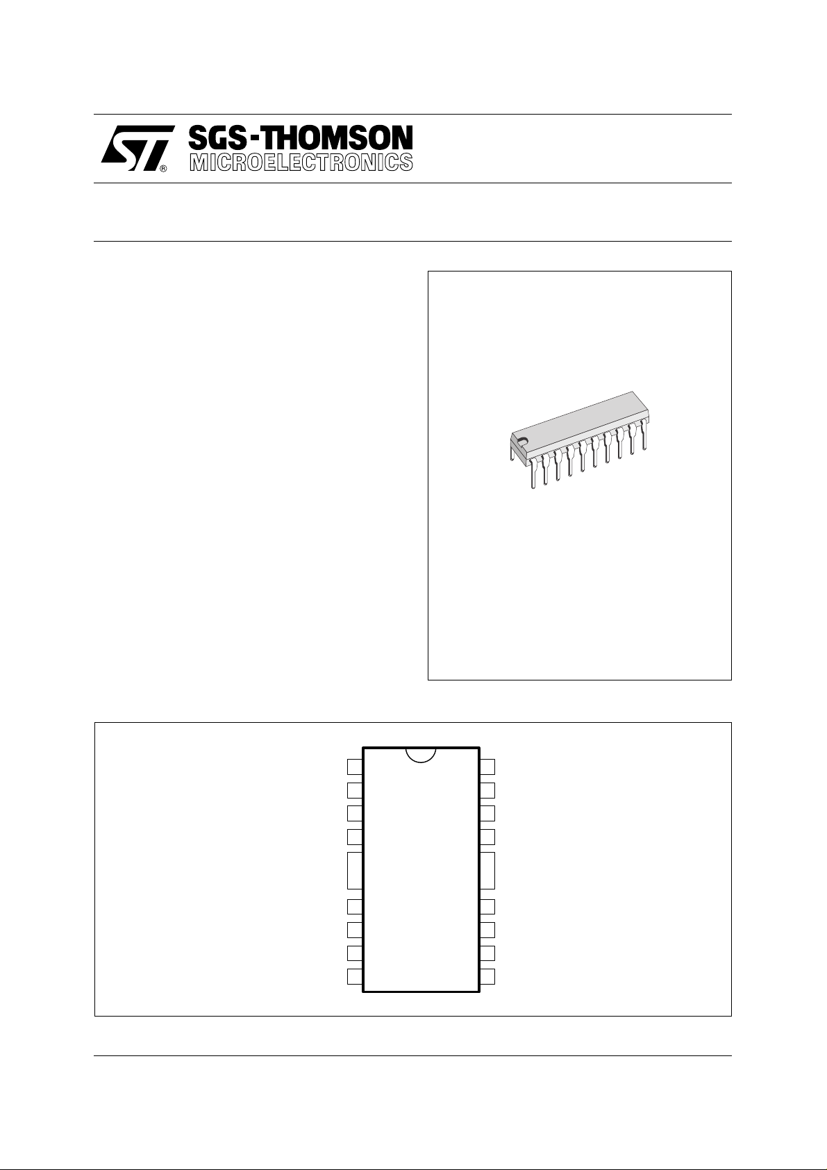
TDA8214B
POWERDIP 16 + 2 + 2
(Plastic Package)
ORDER CODE : TDA8214B
PIN CONNECTIONS
FRAME FLYBACK GENERATOR
POWER AMPLIFIER INPUT
VIDEO IDENTIFICATION OUTPUT
FRAME POWER SUPPLY
September 1993
CC1
FRAME OSCILLATOR
V
CC2
GROUND
GROUND
FRAME OUTPUT LINE OSCILLATOR
1
2
3
4
5
6
7
8
9
10
20
19
18
17
16
15
14
13
12
11
VIDEO INPUTV
SUPER SANDCASTLE OUTPUT
LINE FLYBACK INPUT
LINE OUTPUT
GROUND
GROUND
RC NETWORK
LINE SAWTOOTH INPUT
PHASE DETECTOR
8214B-01.EPS
1/9
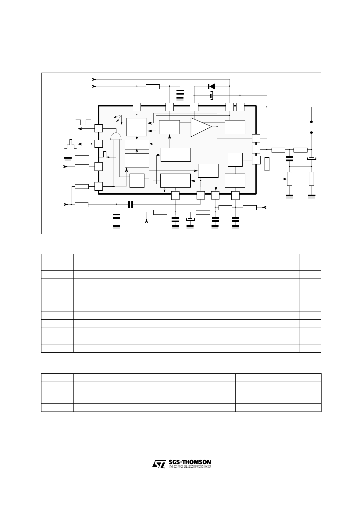
TDA8214B
BLOCK DIAG RAM
Vcc2
Vcc1
12
3
Flyback
generator
Output
stage
Line
oscillator
11
4
YOKE
10
7
17
Vcc1
Video
Identification
Video
Input
Line
Flyback
1
Frame
8
19
2µs
20
18
blanking
detector
Σ
Line flyback
detector
Input
stage
Vcc1
2
Frame
oscillator
Frame-Synchro
generator
Burst gate pulse
generator
2µs
14
9
Power
stage
+
-
Phase
detector
13
ABSOL UT E MAXIM UM R ATINGS
Symbol Parameter Value Unit
1 Supply Voltage 30 V
V
CC
2 Flyback Generator Supply Voltage 35 V
V
CC
V9 Frame Power Supply Voltage 60 V
I10
NR
I10 Frame Output Current (continuous) ± 1A
V17 Line Output Voltage (external) 60 V
17 Line Output Peak Current 0.8 A
I
P
17 Line Output Continuous Current 0.4 A
I
C
T
STG
T
J
T
AMB
Frame Output Current (non repetitive) ± 1.5 A
Storage Temperature -40 to + 150
Max Operating Junction Temperature + 150
Operating Ambient Temperature 0 to 70
o
C
o
C
o
C
8214B-02.EPS
8214B-01.TBL
THERMAL D ATA
Symbol Parameter Value Unit
Max Junction-case Thermal Resistance 10
Typical Junction-ambient Thermal Resistance
(Soldered on a 35µm thick 45cm2 PC Board copper area)
40
Max Recommended Junction Temperature 120
2/9
R
R
TH(j-c)
TH(j-a)
T
J
o
C/W
o
C/W
o
C
8214B-02.TBL

TDA8214B
ELECTRICAL CHARACTERISTICS
V
= 10V, T
CC1
Symbol Parameter Min. Typ. Max. Unit
SUPPLY (Pin 1)
V
I
CC1
Supply Current 15 mA
Supply Voltage 9 10 10.5 V
CC1
VIDEO INPUT (Pin 20)
V20 Reference Voltage (I20 = -1µA) 1.4 1.75 2 V
MWF Minimum Width of Frame Pulse (When synchronized with TTL signal) 50 µs
LINE OSCILLATOR (Pin 11)
LT11 Low Threshold Voltage 2.8 3.2 3.6 V
HT11 High Threshold Voltage 5.4 6.6 7.8 V
BI11 Bias Current 100 nA
DR11 Discharge Impedance 1.0 1.4 1.8 kΩ
FLP1 Free Running Line Period
(R = 34.9kΩ Tied to V
FLP2 Free Running Line Period (R = 13.7KΩ, C = 2.2nF) 27 µs
OT11 Oscillator Threshold for Line Output, Pulse Triggering 4.6 V
∆F
∆θ
Horizontal Frequency Drift with Temperature (see application) 2 Hz/oC
LINE OUTPUT (Pin 17)
LV17 Saturation Voltage (I
OPW Output Pulse width (line period = 64µs) 27 29 31 µs
LINE SAWTOOTH INPUT (Pin 13)
V13 Bias Voltage 1.8 2.4 3.2 V
Z13 Input Impedance 4.5 5.8 8 kΩ
PHASE DETECTOR (Pin 12)
I12 Output Current During Synchro Pulse 250 350 500 µA
RI12 Current Ratio (positive/negative) 0.95 1 1.05
LI12 Leakage Current -2 +2 µA
CV12 Control RangeVoltage 2.60 7.10 V
VIDEO IDENTIFICATION (Pin 8)
Low Level Output when the line syn. tip is centered in the line retrace
V
V
Without video signal (I8 = -500µA) 4.5 6.3 V
H8
With video signal (I8 = 50µA) 0.6 0.9 V
L8
FRAME OSCILLATOR (Pin 2)
LT2 Low Threshold Voltage 1.6 2.0 2.3 V
HT2 High Threshold Voltage 2.6 3.1 3.6 V
DIF2 LT2 - HT2 1.0 V
BI2 Bias Current 30 nA
DR2 Discharge Impedance 300 470 700 Ω
FFP1 Free Running Frame Period
(R = 845kΩ Tied to V
MFP Minimum Frame Period (I20 = -100µA) with the Same RC 12.8 ms
FFP2 Free Running Frame Period (R = 408kΩ, C = 220nF) 14.3 ms
FPR Frame Period Ratio = FFP/MFP 1.7 1.8 1.9
FG Frame Saw-tooth Gain Between Pin 1 and non Inverting Input of the
Frame Amplifier
∆F
∆θ
Vertical Frequency Drift with Temperature (see application) 4.10
= 25oC (unless otherwise specified )
AMB
, C = 2.2nF Tied to Ground)
CC1
= 200mA) 1.1 1.6 V
17
, C = 180nF Tied to Ground
CC1
62 64 66 µs
20.5 23 25 ms
-0.4
-3
Hz/oC
8214B-03.TBL
3/9

TDA8214B
ELECTRICAL CHARACT E RIS TICS (continued)
V
= 10V, T
CC1
Symbol Parameter Min. Typ. Max. Unit
FRAME POWER SUPPLY (Pin 9)
V9 Operating Voltage (with flyback Generator) 10 58 V
I9 Supply Current (V9 = 30V) 11 22 mA
FLYBACK GENERATOR SUPPLY (Pin 3)
V
CC2
FRAME OUTPUT (Pin 10)
LV10A I10 = 0.1A 0.06 0.6 V
LV10B I10 = 1A 0.37 1 V
HV10A I10 = -0.1A 1.3 1.6 V
HV10B I10 = -1A 1.7 2.4 V
FV10A I10 = 0.1A 1.6 2.1 V
FV10B I10 = 1A 2.5 4.5 V
FLYBACK GENERATOR (Pin 3 and Pin 4)
F2DA I
F2DB I
FSVA I
FSVB I
FCI Leakage Current Pin 3 170 µA
SUPER SANDCASTLE OUTPUT (Pin 19)
SANDT2 Frame blanking pulse level 2 2.5 3 V
SANDL2 Line blanking pulse level 4 4.5 5 V
BG2 Burst key pulse level 8 9 V
SC3 Delay between middle of sync pulse and leading edge of burst key pulse 2.3 2.7 3.1 µs
SC2 Duration of burst key pulse
LINE FLYBACK INPUT (Pin 18)
τ RC network time constant (Note 2) 6 µs
Notes : 1. Width of vertical blanking pulse on SSC output is proportional to the frame flyback time, the switching level is VCC2 - 2VBE and
the other input of the comparator is tied to the frame amplifier output. Application circuit uses the frame flyback generator .
2. An RC network is connected to this input. Typical value for the resistor is 27kΩ and 220pF for the capacitor. A different time
constant for RC changes the delay between the middle of the line synchro pulse and the leading edge of the burst key pulse but
also the duration of the burst key pulse.
= 25oC (unless otherwise specified )
AMB
Operating Voltage 10 30 V
Saturation Voltage to Ground (V9 = 30V)
Saturation Voltage to V9 (V9 = 30V)
Saturation Voltage to V9 in Flyback Mode (V10 > V9)
Flyback Transistor on (output = high state), V
= 0.1A 1.5 2.1 V
4 → 3
= 1A 3.0 4.5 V
4 → 3
Flyback Transistor on (output = high state), V
= 0.1A 0.8 1.1 V
3 → 4
= 1A 2.2 4.5 V
3 → 4
Flyback Transistor off (output = V9 - 8V), V9 - V
= 30V V4/3 with
CC2
= 30V V3/4 with
CC2
= 30V
CC2
Output Voltages (R load = 2.2kΩ)
Pulses width and timing
Vertical blanking pulse width
3.7 4
Note 1
5 µs
Switching level 2 V
Maximum imput current at V
= 800V 8 mA
PEAK
Limiting voltage at maximum current 4.3 V
8214B-04.TBL
4/9

TDA8214B
GENERAL DES CRI PTI O N
The TDA8214B performs all the video and power
functions required to provide signals for the line
driver and frame yoke.
It contains:
- A synchr onization separat or
- An integrated frame separator without external
components
- A saw-tooth generator for the frame
- A power amplifier for direct drive of frame yoke
(short circuit protect ed)
- An open collector output for the line driver
Figure 1 : Synchronization Separator Circuit
VR
Video
R1
- A line phase detector and a voltage control osci llator
- A super sandcastle generator
- Video identification output.
The slice level of sync-separat ion is f ixed by value
of the external resistors R1 and R2. V
internally fixed voltage.
The sync-pulse allows the discharge of the capacitor by a 2 x I current. A line sync-pulse is not able
to discharge the capacitor under V
/2. A frame
Z
sync-pulse permits the complete discharge of the
capacitor, so during the frame sync-pulse Q
Q
provide current for the other parts of the circuit.
4
SL1
SL2
20
is an
R
and
3
Figure 2 : Frame Separator
SL1
R2
8214B-03.EPS
Vz
Q3
I
3I
ST1
/2
Vz
Q4
ST2
8214B-04.EPS
5/9

TDA8214B
Figure 3 : Line Oscillator
Vcc1
R5
11
Phase
comparator
output
R4
The oscillator thresholds are internally fixed by
resistors. The discharge of the capacitor depends
on the internal resistor R4. The control voltage is
applied on resistor R5.
Figure 4 : Phase Comparator
Line
Flyback
8214B-05.EPS
comparator is an alternat ively negative and positive
current. The frame sync-pulse inhibits the comparator to prevent frequency drift of the line oscillator
on the frame beginning.
Figure 5
Vcc1
12
13
Integrated
Flyback
Sync pulse
Output
Current
Vc
The sync-pulse drives the current in the comparator. The line flyback integrated by the external net
work gives on pin 13 a saw tooth, the DC offset of
this saw tooth is fixed by VC. The comparator
output provides a positive c urrent for the part of the
signal on pin 13 greater t han to V C and a negative
current for the other part. When t he line flyback and
the video signal are synchronized, the output of the
6/9
SL2
ST1
8214B-06.EPS
Line output (Pin 17)
It is an open-collector output. The output positive
pulse time is 29µs for a 64µs period.
The oscillator thresholds are internally fixed by
resistors. The oscillator is synchronized during the
last half free run period. The input current during
the charge of the capacitor is less than 100nA.
Vc
8214B-07.EPS

Figure 6 : Frame Oscillator
INPUT CURRENT
COMPENSATION
2
TDA8214B
Vcc1
Frame
sync pulse
To frame amplifier
Frame output amplifier
This amplifier is able to drive directly the frame
yoke. Its output is short circuit and overload protected; it contains also a thermal protect ion.
The frame blanking is detected by the frame flyback generator. When the output voltage of the
frame amplifier exceeds V
2-2VBE, the pulse is
CC
detected. The line flyback detect ion is provided by
a comparator which compares the input line flyback
pulse to an internal ref erence. The burst gate pulse
position is fixed by the external RC network
(Pin 14). It is referenced to the middle of the line
Figure 7 : Super Sandcastle Generator
Line
Flyback
Vcc1
Input
18
Frame
Output
10
YOKE
Line
Flyback
Detection
Frame
Blanking
Detection
flyback.
This stage will detec t the coincidenc e bet ween th e
line sync pulse (if present) and a 2µs sampling
pulse. This 2µs pulse is positionned at the center
of line sync pulse when the phase loop is locked.
This sampled detection is stored by an external
capacitor Pin 8.
The identification output level is high when video
signal is present.
Important remark : minimum saw-tooth amplitude
on Pin 13 has to be 2V
Σ
Burst gate
pulse
generator
RC
400 µ A
(typ. : 2.5VPP).
PP
Vcc1
19
SSC
Output
8214B-08.EPS
RC
Network
14
8214B-09.EPS
7/9

TDA8214B
Figure 8 : Video Identification Circuit (Pin 8)
V
13
H
2.75V
V
L
2.25V
5.8kΩ
V
CC1
Line retrace
V
R
2.5V
V
CC1
12µs
Line
Flyback
Integrated
Flyback
V
H
V
L
V
R
10kΩ
Video
Ident.
Output
1N4148
BC547
10µF
TYPICAL APPLICATION
100
220nF
560kΩ
15k
Ω
68pF
100k
180pF
4.7
100nF
µF
22nF
22nF
Ω
4.7k
1µF
Video
Input
Vcc
+24V
Vcc1
27k
Ω
220pF 180nF
1.5k
Ω
120pF
Line
Flyback
1kΩ
8
Ω
100nF
820kΩ
µ
10
2 1 8 3 9 4
14
20
10kΩ
IN4148
F
470
µ
F
BC547
TDA 8214B
13
18
12
Ω
12nF
100k
2.2nF
11 5 6
Ω
22k
Ω
Vcc1
22k
Ω
Horizontal
Frequency
15
SSC
Sampling Pulse
V
R1
Line Sync.
IN4002
47µF
19 17
16
2.2k
Ω
Line
Sync.
V
R1
Video Identification
IN4148
10
7
680pF
Vcc1
100
220k
22k
Vertical
Ω
Amplitude
I8
Ω
220nF
Ω
100nF
Frame Yoke
30 mH, 15
I = 840mA
pp
220k
100
Ω
Ω
Ω
with video
without video
2.2
Ω
270
1000µF
1
Ω
8214B-10.EPS
Ω
8214B-11.EPS
8/9
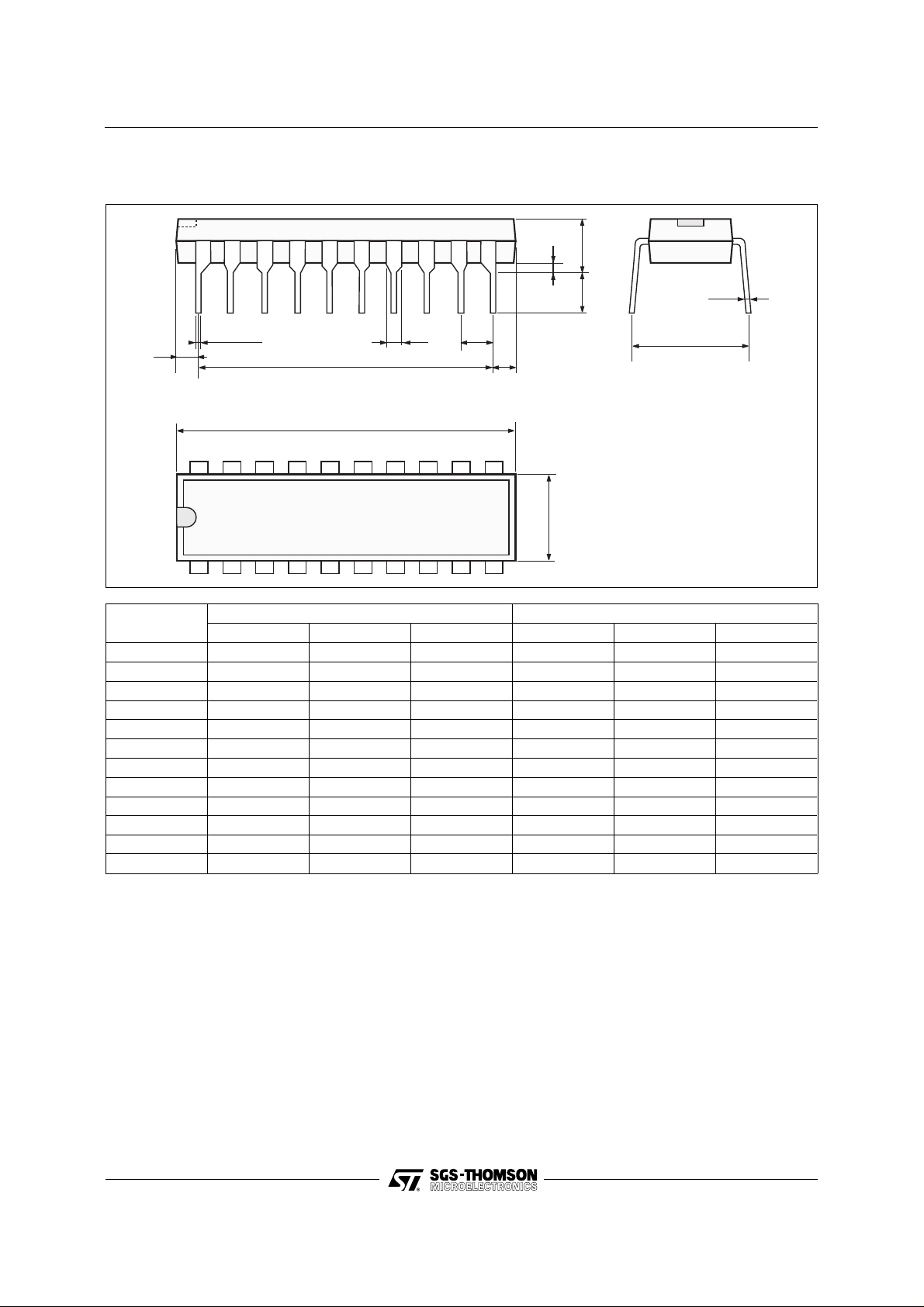
PACKAGE MECHANICAL DATA
20 PINS - PLASTIC POWERDIP
TDA8214B
I
a1
L
Z
e3
b
B
e
E
Z
D
20 11
F
110
Dimensions
Min. Typ. Max. Min. Typ. Max.
a1 0.51 0.020
B 0.85 1.4 0.033 0.055
b 0.5 0.020
b1 0.38 0.5 0.015 0.020
D 24.8 0.976
E 8.8 0.346
e 2.54 0.100
e3 22.86 0.900
F 7.1 0.280
i 5.1 0.201
L 3.3 0.130
Z 1.27 0.050
Millimeters Inches
b1
PMDIP20W.EPS
DIP20PW.T BL
Information furnished i s believed to be accurate and rel iabl e. However, S GS-THOMSON Microel ectroni cs assumes no responsibil ity
for the consequences of use of such information nor for any infringemen t of patents or other rights of third parties which may result
from its use. No licence is granted by implication or otherwise under any patent or patent rights of SGS-THOMSON Microelectronics.
Specifications mentioned in this publication are subject to change without notice. This publication supersedes and replaces all
information previously supplied. SGS-THOMSON Microelectronics products are not authorized for use as critical components in life
support devices or systems without express written approval of SGS-THOMSON Microelectronics.
© 1994 SGS-THOMSON Microele c tronics - All Rights Reserved
2
Purchase of I
2
C Patent. Rights to use these components in a I2C system, is granted provided that the system conforms to
I
Australia - Brazil - China - France - Germany - Hong Kong - Italy - Japan - Korea - Malaysia - Malta - Morocco
The Netherlands - Singapore - Spain - Sweden - Switzerland - Taiwan - Thailand - United Kingdom - U.S.A.
C Components of SGS-THOMSON Microelectronics, conveys a license under the Philips
2
C Standard Specifications as defined by Philips.
the I
SGS-THOMSON Microelectroni cs GROUP OF COMPANIES
9/9
 Loading...