

.
VERYLOWCURRENT ABSORPTION
.
3 STAGEIFGAIN CONTROLLED AMPLIFIER
.
SYNCHRONOUS VIDEODEMODULATOR
.
WHITE SPOTANDNOISE INVERTER
.
AGCCIRCUIT WITH NOISE GATING
.
TUNERAGCOUTPUTFORPNP TUNERS
.
FM DETECTOR
.
AF AMPLIFIER WITH DC VOLUME CONTROL
.
AFC
.
2VPPONVIDEOOUTPUT
DESCRIPTION
The TDA8213 is a monolithic integrated circuit in
DIP20 package for colourand black & white television receivers using PNP tuners. It is intendedto
operate with a negativelymodulated vision carrier
and frequencymodulated soundcarrier.Used with
TDA8214/15 (H/Vdeflection circuit)and TDA8217
(Pal decoderand videoprocessor), this IC permits
a completelow-cost solution for PALapplications.
TDA8213
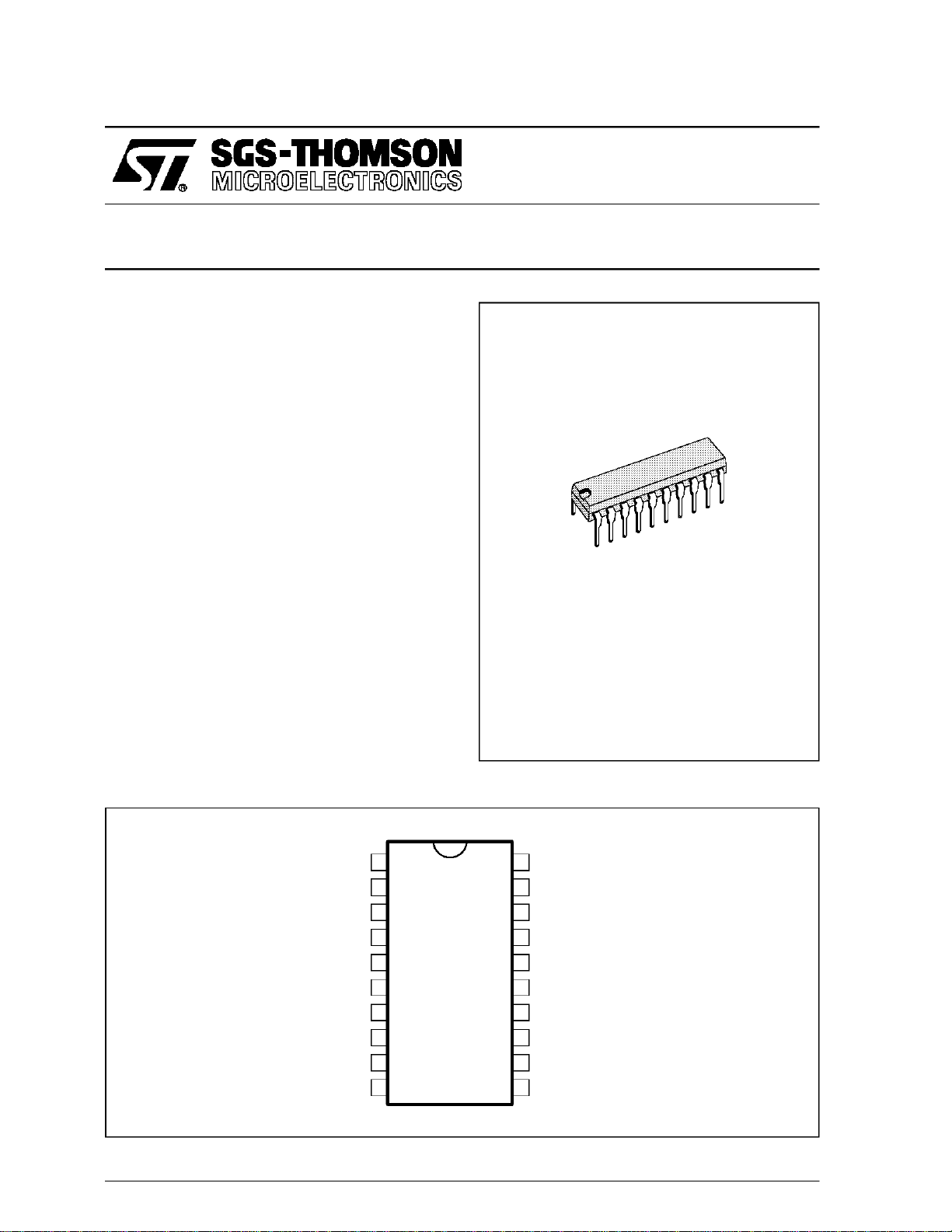
VIDEO & SOUND IF SYSTEM
DIP20
(Plastic Package)
ORDER CODE : TDA8213
PIN CONNECTIONS
TUNER DELAY RESISTOR
TUNER OUTPUT CURRENT
NOT TO BE CONNECTED
SOUND VOLUME CONTROL
October 1993
V
CC
IF INPUT
IF INPUT
GROUND
AUDIO OUTPUT
FM TANK LC
1
2
3
4
5
6
7
8
9
10
20
AGC MEMORY CAPACITOR
19
IF LC
18
IF LC
17
VIDEO PEAKING
16
AFC TANK LC
15
AFC OUTPUT
14
CVBS OUTPUT
13
NOT TO BE CONNECTED
12
2nd IF SOUND CHANNEL INPUT
11
2nd IF SOUND CHANNEL INPUT
8213-01.EPS
1/8
TDA8213
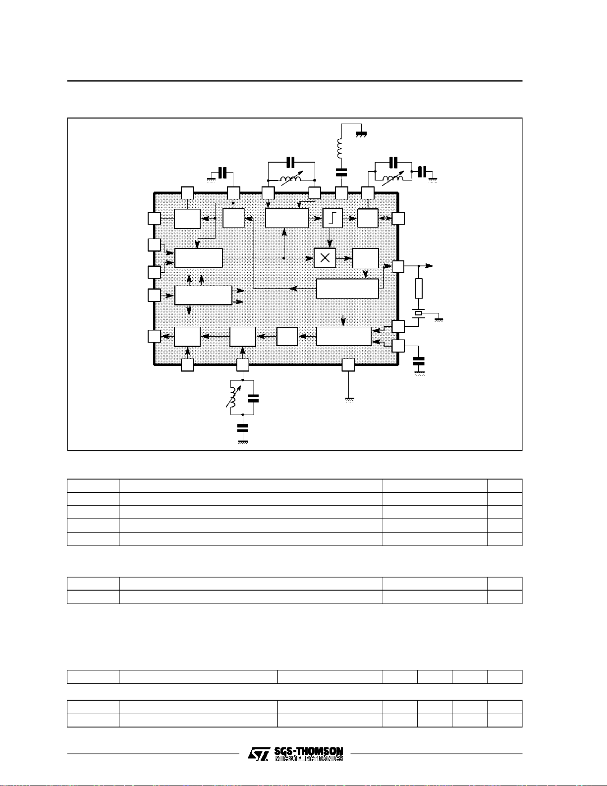
BLOCK DIAGRAM
I tuner
Out
I.F. Input
I.F. Input
Vcc
9V
Audio
Output
2
5
6
3
8
38.9 MHz
VIDEO
peaking
38.9 MHz
RTD
17
1
TUNER
DELAY
3 I.F. AMPLIF.
Band Gap reference
Voltage
Volume
Control
910 7
A.G.C.
DISCR.
F.M.
1920
REFERENCE
AMPLIFIER
L.P.F.
18
WHITE& NOISE
SPOT INVERTER
4 STAGE LIMITER
16
A.F.C.
Video
Amplif.
5.5MHz
AFC
15
Output
CVBSOutput
14
12
11
5.5MHz
ABSOLUTEMAXIMUM RATINGS
Symbol Parameter Value Unit
V
S
V
X
P Power dissipation at T
T
STG
Supply voltage 13.5 V
Tuner AGC voltage V
=70oC 880 mW
AMB
S
Storage temperaturerange - 40, + 150
THERMALDATA
Symbol Parameter Value Unit
R
TH(j-a)
Junction-ambient thermal resistance Max. 80
ELECTRICALCHARACTERISTICS
=25oC, VCC= 9V, IF input = 10mV
(T
amb
Soundcarrierinput : 5.5MHz,10mV
RMS,fm
top sync,D =90%, Video BW = 5MHz,
RMS
= 1kHz, AudioBW = 20kHz, ∆f=±25kHz,
Volumeattenuation = 0dB,unless otherwisespecified)
Symbol Parameter Test conditions Min. Typ. Max. Unit
SUPPLY
Supply voltage 8 9 12.8 V
Supply current 14 20 28 mA
o
o
C/W
8213-02.EPS
V
C
8213-01.TBL
8213-02.TBL
8213-03.TBL
2/8
TDA8213
ELECTRICAL CHARACTERISTICS
=25oC, VCC= 9V, IF input= 10mV
(T
amb
Sound carrier input : 5.5MHz, 10mV
RMS,fm
Volumeattenuation =0dB, unlessotherwise specified)
Symbol Parameter Test conditions Min. Typ. Max. Unit
IF AMPLIFIER
AGC range 58 64 67 dB
IF - sensitivity (RMS) Video out -3dB 70 µV
R input differential
C input Stray 2pF
DEMODULATED VIDEO OUTPUT
S/N video (BW = 5MHz)
Intermodulation 1.07MHz AGC open loop, Picture carrier = 0dB,
Detected video output peak to
peak (positive)
Topsynchro output level 1.9 V
Video Bandwidth with output filter -3dB, see Figures 1 and 2 7 MHz
Differential phase 3 7 Degree
Differential gain 37 %
White noise clamp
White noise insertion 3.2 V
Video output current capability 1.2 2 2.6 mA
Residual output carrier (RMS) At 38.9MHz
AFC
AFC slope With R
AGC CIRCUIT
Maximum I charge 550 900 1200 µA
Maximum I discharge 14 20 26 µA
I
CH /IDISCH
TUNER AGC
Sinked Current Suitable for Mosfet-NCH 1.15 2 2.6 mA
Slope RTD = 0 ÷ 10kΩ 600 µA/dB
DEMODULATED AUDIO OUTPUT
Detected output audio signal (RMS) 120 270 350 mV
Totalharmonic distorsion 0.5 2 %
Amplitude modulation rejection m = 30% 40 53 dB
2nd IF sound sensitivity -3dB FM
detected audio signal (RMS)
S + N
N
Thermal drift of volume 0.05 dB
Input resistance limiter 400 560 720 Ω
VolumeControl versus V
Ratio 45 -
9
top sync, D = 90%, Video BW= 5MHz,
RMS
=1kHz, Audio BW = 20kHz, ∆f=±25kHz,
Guaranteed by process
V
9
V
9
(WH − BL)
10
= 2.5V
= 0.9V
N
RMS
IF inp. = 10mV
RMS
, 20 log
Chrominance carrier = -3.2dB,
Sound carrier = -20dB
Referred to the videooutput
see Figure 6
At 77.8MHz
= 200kΩ, see Figure 3 25 40 60 mV/kHz
Load
∆f=±25kHz for signal
∆f= 0 after deemphasis (BW = 20kHz)l
See Figure 4 V9= 4.5V
1 1.5 2 kΩ
49 55 dB
50 dB
1.8 2 2.4 V
4.5 V
10
20
200 µV
50 60 dB
0
12
187424
65
mV
mV
o
dB
dB
dB
C
8213-04.TBL
3/8

TDA8213
TEST CIRCUIT
9V
VIF
Input
38.9 MHz
M = 100 %
R = 10%
AMDSB
10nF
4
200
Ω
4
10 nF
AUDIO
SIGNAL
WITHOUT
DEEMPHASIS
AUDIOOUTPUT
WITH DEEMPHASIS
L
µ
10
100nF
5
6
7
47nF
9VDC
F
IoT
µ
10
H
3
TDA 8213
8
9 10 11
Ω
1k
4.7µH
4.7kΩ
V1TUN
A
17
100
10k
27pF
100pF
C
Ω
1µF
Ω
B
5.5MHz
Q>40
100nF
SW1
1.8k
47pF
100nF
Ω
220
2.2k
38.9MHz
18192012
100nF
Ω
Ω
180
Q=80
16
15
14
12
6.2 Vz
Ω
38.9 MHz
Q=80
47pF
470nF
10nF
9V
Video
Out 1
100k
100k
E
Ω
AFC
D
Out
Ω
F
33nF
I
Volume
control
Ω
50
FM Input
Video
Out 2
8213-03.EPS
Figure 1 : Output Signal Bandwidth without
Video peaking
V (dB)
OUT
0
-3
-6
-9
-12
-15
0246810
4/8
F (MHz)
Figure2 : OutputSignal Bandwidth with Video
peaking
V (dB)
OUT
0
-3
-6
-9
-12
-15
8213-04.EPS
0246810
F (MHz)
8213-05.EPS

TDA8213
Figure3 : AFC Voltageversus Input Frequency
Figure4 : Volume ControlAttenuationversus
Voltagein Pin 9
AFC OUTPUT
VOLTAGE (V)
8
6
4
2
0
38.5 39.338.7 38.9 39.1
IF FREQUENCY
(MHz)
-20
-40
-60
-80
-100
ATTENUATION
8213-06.EPS
(V)
123450
Figure5 : TypicalConnection from µP to TDA8213for Remote VolumeControl (Pin 9)
Processor
Pushpull
Output
10kΩ
TDA8213
9
V (V)
9
8213-07.EPS
ST63XX
Figure 6 : Blackand WhiteNoise Inverter
V (V)
14
4.5
3.9
3.2
2.5
1.9
1.3
C
80k
Ω
8213-08.EPS
White spike noise clamp
Top white
White noise levelinsertion
Noise level insertion
Top synchronization
Black spikes noise clamp
t(s)µ
8213-09.EPS
5/8

TDA8213
Figure 7 : TypicalApplication
10nF27pF
47pF
Ω
AFC
Output
200k
S
V
Video
Output
µF
1
TunerAGCOUT
Q=80
38.9MHz
100nF
10µF
47pF
Ω
3.9k
10µF
15
7
200kΩ
14
12
11
109
8
µH
15
56pF
1kΩ
BPF
1.2kΩ
Q>40
5.5MHz
100nF
100pF
33nF
DC
Audio
47nF
Control
Volume
Output
5.5MHz
Q=80
38.9MHz
16
4.7µH
1819 17
Ω
1.8k
1µF
120
10kΩ
23
TDA8213
6
4
55
6/8
3
OFW
1nF
G1959
2
1
BF959
560Ω
Ω
51
3.3kΩ
1nF
IF
IN
9.1V
Ω
S
V = 12V
100
H
µ
10
100nF 100nF
1µH
10µF
H
µ
10
4.7kΩ 1kΩ 10kΩ
10nF
Ω
100
560Ω
8213-10.EPS

Figure8 : PC Board and ComponentsLay-out of theCircuit of Figure 7 (1 : 1 scale)
TDA8213
8213-11A.TIF/8213-11B.TIF
7/8

TDA8213
PACKAGE MECHANICALDATA
20 PINS - PLASTICDIP
I
a1
L
Z
Dimensions
b
e3
20 11
110
B
D
Millimeters Inches
Min. Typ. Max. Min. Typ. Max.
e
Z
F
E
a1 0.254 0.010
B 1.39 1.65 0.055 0.065
b 0.45 0.018
b1 0.25 0.010
D 25.4 1.000
E 8.5 0.335
e 2.54 0.100
e3 22.86 0.900
F 7.1 0.280
i 3.93 0.155
L 3.3 0.130
Z 1.34 0.053
b1
PM-DIP20.EPS
DIP20.TBL
Information furnished is believed to be accurate and reliable. However, SGS-THOMSON Microelectronics assumes no responsibility
for the consequences of use of such information nor for any infringement of patents or other rights of third parties which may result
from its use. No licence isgranted by implication or otherwiseunder anypatent or patent rights of SGS-THOMSON Microelectronics.
Specifications mentioned in this publication are subject to change without notice. This publication supersedes and replaces all
information previously supplied.SGS-THOMSON Microelectronics products are not authorized for useas critical components in life
support devices or systems without express written approval of SGS-THOMSON Microelectronics.
1994 SGS-THOMSON Microelectronics - All Rights Reserved
Purchase of I
2
I
C Patent.Rights to usethese components in a I2C system, is granted provided that the system conforms to
Australia - Brazil - China - France - Germany - Hong Kong - Italy -Japan - Korea - Malaysia - Malta - Morocco
The Netherlands - Singapore - Spain - Sweden - Switzerland -Taiwan - Thailand - United Kingdom - U.S.A.
2
C Components of SGS-THOMSON Microelectronics, conveys a license under the Philips
2
the I
C Standard Specifications as defined by Philips.
SGS-THOMSON Microelectronics GROUP OF COMPANIES
8/8
 Loading...