

.
HIGHLY INTEGRATED TWO CHIP SOLUTION FOR NICAM DEMODULATION (using
TDA8204 decoder)
.
AUTOMATIC DUAL STANDARD DE MOD ULATION 6.552MHz FOR I SYSTEM
5.85MHz FOR B/G SYSTEM
.
40dB RANGE A GC
.
SINGLE CRYSTAL OPERATION
.
NICAM 728 DATA AND CLOCK RECOVERY
.
LOW PASS FILTER FOR PWM CODED
AUDIO SIGNALS AND J-17 DE-EMPHA SI S
.
AUTOMATIC FM MONO SELECTION BY RESERVE SOUND SWITCH FUNCTION
.
VERSATILE A UDI O SWI T CHING MATRI X
.
AUTOM ATIC MUTE FUNCTION
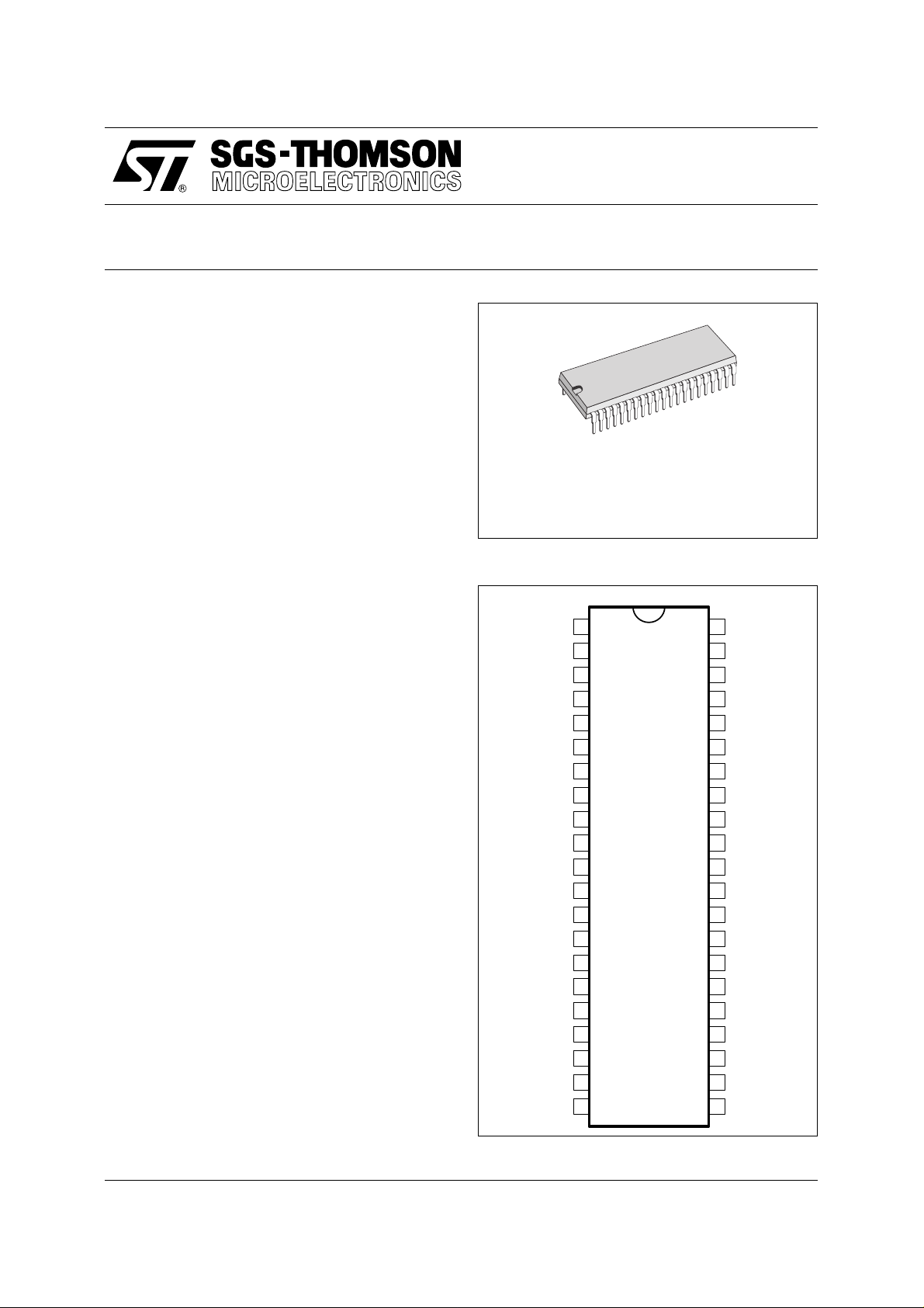
TDA8205
NICAM QPSK DEMODULATOR
SHRINK 42
(Plastic Package)
ORDER CODE : TDA8205
PIN CONNECTIONS
DESCRIP TION
The TDA8205 is es sentially divided into two s ignal
processing sections. The first section handles all
the NICAM signal acquisition, the QPSK demodulator and clock and data recovery circuits. The key
point to note about this section is the dual frequency synthesiser. By use of only one quartz
crystal, the IC is able to demodulate QPSK signals
from either system I or system B/G in an automatic
way . The second section of the TDA8205 manages
the analog parts of the twin digital-to-analog converters (DA Cs) and all filter ing and audio switc hing
downstream of the DACs. A simple serial bus from
the TDA8204 allows control of the s witch f unctions
by the CTV system microcontroller.
GND
XC1
XC2
DF2
DF1
BG
AGC
V
V
LFIL1
RG
GND
RFIL1
RESET
V
SERI
DACDL
DACDR
GND
CK11648 CK728
I
CC
DD
DD
1
2
3
4
5
6
IN
7
IN
8
9
10
11
12
13
14
15
16
17
18
19
20
21
LF1
42
LF2
41
XK1
40
V
39
38
37
36
35
34
33
32
31
30
29
28
27
26
25
24
23
22
CC
EAIR
EAIL
SAIR
SAIL
MAI
CAP
AMOR
AMOL
DC2
DC1
AOR
AOL
GND
MMO
TEST
NDO
8205-01.EPS
October 1993
1/8
TDA8205
PIN AS SIG MENT
Pin No Pin Name Function Pin No Pin Name Function
1 GND Ground 22 CK728 728kHz Clock Intput
2 XC1 Optional Crystal 23 NDO NICAM Data Output
3 XC2 Optional Crystal 24 TEST To be connected to GND
4 DF2 Data Filter 2 (eye monitor) 25 MMO Matrix Mute Out
5 DF1 Data Filter 1 (eye monitor) 26 GND Ground
6BG
7I
IN
8 AGC AGC Filter Capacitor 29 DC1 Decoupling 1
9V
10 V
CC
DD
11 LFIL1 Left Filter 1 (J-17 De-emphasis) 32 AMOR Audio Mutable Output Right
12 RG Gain Setting Resistor for DAC 33 CAP Decoupling Capacitor
13 GND Ground 34 MAI Mono Audio Input
14 RFIL1 Right Filter 1 (J-17 De-emphasis) 35 SAIL Stereo Audio Input Left
15 RESET Reset Chip 36 SAIR Stereo Audio Input Right
16 V
DD
17 SERI Interchip Serial Bus Input 38 EAIR External Audio Input Right
18 DACDL DAC Data Left Input 39 V
19 DACDR DAC Data Right Input 40 XK1 11.648MHz Crystal
20 GND Ground 41 LF2 Loop Filter 2
21 CK11648 11.648MHz Clock Output 42 LF1 Loop Filter 1
System B/G Input 27 AOL Audio Output Left
IN
System I Input 28 AOR Audio Output Right
+12V Supply 30 DC2 Decoupling 2
+5V Supply 31 AMOL Audio Mutable Output Left
+5V Supply 37 EAIL External Audio Input Left
CC
+12V Supply
8205-01.TBL
BLOCK DIAG RAM
DD
DD
CC
V
V
V
39 8 5 4 42 23 22211918 11 343536 31 32 37 38
16
10
AGC
AGC
1
GND
DF1
DF2
QSPSK
DEMOD
DUAL FREQ
SYNTHESISER
20 17331412
GND GND GND
LF1
RECOVERY
2613
LF2
419
CLOCK
& DATA
2 340
XC1
NDO
XC2
CK728
XK1
BG
TEST
RESET
7
I
IN
6
IN
24
15
CC
V
SWITCH
TDA8205
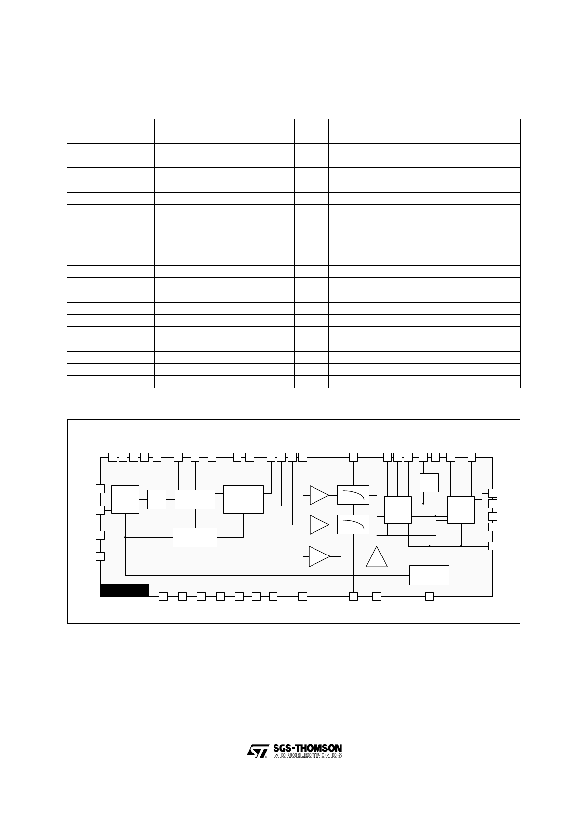
BLOCK DIAG RAM DES CRI PTI ON
The QPSK signal enters the IC via two inputs after
passing through two external bandpass filters at
the relevant frequencies of 6.552MHz and
5.85MHz for system I and B/G respectively. The
two inputs enter a source selection switch and pass
immediately to an AGC block which has a total
range of 40dB. The resulting levelled signal passes
CK11648
DACDR
DACDL
DAC
DAC
RG RFIL1 CAP
LPF
LPF
MAI
SAIR
LFIL1
SAIL
MUTE
SWITC H
SERI AL
INTERFACE
SERI
EAIL
AMOR
AMOL
MATRIX
SWITCH
to the QPSK demodulator which recovers the NICAM 728Kb/s data stream by means of carr ier and
clock recovery circuits.
Carrier recovery is achieved with a baseband remodulator which consists of a phase locked loop
with a switchable phase detector. This allows it to
lock to one of four possible phases of the QPSK
EAIR
27
AOL
AOR
28
DC1
29
DC2
30
MMO
25
8205-02.EPS
2/8
TDA8205
carrier without disruption due to the modulation.
Dual frequency operation is made pos sible by synthesising the carrier reference fre quency thus saving the need for two extra crys tals. Dual VCXO ca n
also be software selected (SYN bit of CR3 in
TDA8204) with external crystal (Pin XC1/XC2) for
new standards. Selection between XC1 and XC2
is done with bit "IBG" in CR3 register of TDA8204
(IBG = 0 XC1 selected, IBG = 1 XC2 selected).
The standards switch controls operation of the
QSPK demodulator at either 6.552MHz or
5.85MHz. This can be controlled via the I
2
C bus or
the decoder set into automatic mode in which it
determines the standard by alternately trying to
lock to the two system s.
On chip low pass filters recover the in-phase and
quadrature data channels which are then sliced by
comparators. The symbol clock is recovered from
this data and used to sample and re-time it. The
two data channels are then decoded and serialized
to obtain the NICAM -728 data which is then pass ed
on to the NICAM decoder in the TDA8204.
After proces sing the NICAM into a digital bit-stream
in the TDA8204, the data is passed back to the
TDA8205 for the analog functions of the DACs to
be performed.
Conversion of the pulse width modulated bit
streams to analog takes place and is followed by
low pass filtering which removes high frequency
quantising noise and performs J-17 de-emphasis.
The DACs signal level can be adjusted to match
the reserve sound signal level.
1V
maximum on Pins LFIL1/RFIL1 can be ob-
RMS
tained by selection of appropriate resistor on
Pin RG.
Once the analog audio has been recovered, certa in
source switch functions are performed. If the NICAM signal fails and if the reserve sound flag (C4),
of SRO register, is set the reserve sound switch
automatically selects Mono Audio Input. If the reserve sound flag (C4) is reset, the reserve sound
switch will not change and the audio outputs will b e
muted (DAC outputs muted).
If the NICAM signal only carries data, Mono Audio
Input is selected. The reserve sound switch can b e
forced to select Mono Audio Input via I
2
C bus , us ing
Bit FS0 = 1 and FS1 =0 of CR3 Register.
This can be used in the case of NICAM marginal
reception. To select Stereo Left and Right Audio
Input Bit FS0 = 0 and FS1 = 1 of CR3 Regis ter must
be selected. The outputs from this reserve sound
switch are available on Audio mutable output left
and right, and are internaly connected to the audio
matrix.
A simple audio switching matrix is provided internally for flexible control over the audio source and
destination sel ection.
Audio signal left and right com ing f rom the reserv e
sound switch and the external audio input left and
right can be switched to the audio outputs left and
right .
DAC and auxiliary audio outputs can be muted. An
additional +6dB gain can be applied to raise the
output levels to 2V
maximum. For more infor-
RMS
mation see Software Specification chapter (III.5.3/TDA8204).
The DAC outputs are automatically muted under
the following conditions
- loss of frame alignement
- the bit error rate (Ber) is > error rat e limit
- NICAM signal is conveying M1 only. The right
DAC is muted unless M1 has been selected t o be
on both DAC outputs.
- NICAM signal is conveying data only.
For test purposes, the DAC outputs can be unmuted by forcing the bi-directional mute Pin 25 of
TDA8204 or via I
2
C bus.
ABSOLUTE MAXIMUM RATINGS
Symbol Parameter Value Unit
V
CC
V
DD
P
tot
T
oper
T
stg
Supply Voltage 15 V
Supply Voltage 7 V
Total Power Dissipation 1.2 W
Operating Temperature Range 0, + 70
Storage Temperature Range -20, + 150
THERMAL DATA
Symbol Parameter Value Unit
R
th (j-a)
Thermal Resistance Junction-Ambient Max. 67
o
C/W
o
C
o
C
8205-02.TBL
8205-03.TBL
3/8

TDA8205
ELECTRICAL CHARACTERISTICS (T
= 25oC, VCC = 12V, VDD = 5V , unless otherwise specified)
amb
Symbol Parameter Min. Typ. Max. Unit
SUPPLY
V
CC
V
DD
I
CC
I
DD
Supply Voltage Range 11.4 12 12.6 V
Supply Voltage Range 4.75 5 5.25 V
Supply Current 18 36 50 mA
Supply Current 10 18 42 mA
DIGITAL PINS
OUTPUTS
CK11, NDO
V
OL
V
OH
Low Level Output Voltage (I = -4mA) 0.4 V
HIgh Level Output Voltage (I = 4mA) 0.7 V
DD
V
MMO (open collector)
V
OL
I
LK
Low Level Output Voltage (I = -1mA) 0.4 V
High Level Output Current (leakage) ± 2 µA
INPUTS
SERI, DACDL, DACDR, CK728
V
IL
V
IH
I
LK
Low Level Input Voltage 0.8 V
High Level Input Voltage 0.6 V
DD
V
Input Leakage Current ± 2 µA
ANALOG PINS
I-B/G SELECTOR
V
DC
R
IN
C
IN
DC Bias Voltage 2.8 V
Input Resistance 10 kΩ
Input Capacitance 10 pF
AGC
V
IN
AGClv AGC Low Voltage (VIN = 1VPP)2V
Input Voltage Range 10 200 1000 mV
PP
PP
AGChv AGC High Voltage (VIN = 10mVPP)11V
AGCta AGC Attack Time (V
AGCtd AGC Decay Time (V
= 10mV to 1V, C
IN
= 1V to 10mV, C
IN
= 100nF) 15 ms
AGC
= 100nF) 220 ms
AGC
QPSK DEMODULATOR (LF1)
V
DC
DC Bias Voltage (SYN = 1) 1 5 10 V
Kd Phase Detector Constant (no mod.) 33 µA/rad
kv VCO Constant 3.5 MHz/V
EYE DIAGRAM MONITORS (DF1, DF2)
V
DC
R
OUT
V
OUT
DC Bias Voltage 2.5 V
Output Resistance 1.2 kΩ
Output Voltage (System I) 0.6 V
PP
CLOCK AND DATA RECOVERY (LF2)
V
DC
DC Bias Voltage 2.5 V
Kd Phase Detector Constant (all 1’s) 7 µA/rad
kv VCXO Constant 4.4 kHz/V
8205-04.TBL
4/8

TDA8205
ELECTRICAL CHARACTERISTICS (continued)
Symbol Parameter Min. Typ. Max. Unit
DAC AND FILTER (LFIL1, RFIL1)
V
DC
I
OUT
V
RG
AUDIO MATRIX (AOL, AOR, AMOL, AMOR)
V
OUT
S/N Relative to 0.5V
THD 1kHz at 0.5V
Chm Maximum Channel Matching Error 2 dB
S/N Relative to 0.5V
THD 1kHz at 0.5V
Chm Maximum Channel Matching Error 2 dB
DC Bias Voltage 2.5 V
Output Current (RG = 5.6kΩ, DAC full scale) 340 µA
RG Pin DC Voltage 1.25 V
DAC SELECTED
Output Voltage (1kHz at -11.75dB, J17 de-emphasis, RG = 5.6kΩ) 0.39 0.5 0.63 V
, noise measured with IEC-179 A-filter 60 70 dB
RMS
, RG = 5.6kΩ 0.05 0.2 %
RMS
Crosstalk at 1kHz, 0.5V
RMS
65 dB
MONO OR STEREO AUDIO INPUT SELECTED (MAI, SAIL, SAIR)
, noise measured with IEC-179 A-filter 88 dB
RMS
RMS
0.02 %
STEREO AUDIO INPUT SELECTED
Crosstalk at 1kHz, 0.5V
RMS
75 dB
PP
RMS
8205-05.TBL
5/8

TDA8205
APPLICATION DIAG R AMS
Figure 1 : Stand Alone Application (I sta ndard)
LED2LED3LED4
AUDIO
OUTPUT
R
L
FM MONO IN
ERROR
MONITOR
Sele ction
Language
LK1 LK2
LED1
Ω
R17 330
F
µ
C21
10
F
µ
C20
10
F
µ
C24 1
C25 1µF
C19
100nF
X1
11.648 MHz
C11 150pF
C12 18pF*
* C12 value depends on X1
22
28 27 26 25 24 23
29
35 34 33 32 31 30
36
mute
42 41 40 39 38 37
Ω
22
28 27 26 25 24 23
29
35 34 33 32 31 30
36
42 41 40 39 38 37
C10 6.8nF
Ω
R10 39k
IC1 TDA8205 IC2 TDA8204
C9 120pF
C8
220nF
R9 8.2M Ω
C7
100nF
21
15 16 17 18 19 20
14
C28
100nF
8 9 10 11 12 13
7
1 2 3 4 5 6
R19 270
21
15 16 17 18 19 20
14
Q2
8 9 10 11 12 13
7
Ω
R18 10k
1 2 3 4 5 6
C7 680pF
R8
150Ω
dual
FM mono
C17 100nF
100nF
6.552MHz
470Ω
Ω
8.2k
mono
(forced)
C4 1nF
C3 10nF
mono
R16
1MΩ
C16
10µF
C18
100nF
C15
R15
5.6kΩ
Ω
R14
43k
Ω
R13
43k
C14
R12
5.6kΩ
L1
MON1
MON2
R7
470Ω
BFP
C2 10nF
Q1
TRAP
R2 470Ω
C1
10nF
IN
SYS. I
NICAM
single
R11 5. 6kΩ
C13
F1
R4
R1
DAC
(forced)
Unmute
stereo
Q1, Q2 : BC109 or BC550C
F1 : TOKO TH316BQM2110QDAF (5VFP)
T1 : Matsushita EFCS6R0MWS
X1 : 11.648MHz Crystal NDK
Ω
R20 22k
6.8nF
6.8nF
H
µ
10
C6
220pF
C5
220pF
Ω
R6
33
R5
100Ω
Ω
R3
1.2k
F
µ
C26
220
H
µ
F
L2 10
µ
C23
10
DD
V
CC
V
F
µ
C22
10
T1
6.0MHz
8205-03.EPS
6/8

Figure 2 : I2C Bus Controlled Application (I and B/G standar d)
LED2
LED3
mono
single
DD
V
22
ERROR
MUTE
FID
PDV
ADV
DV
SEL1
SEL0
TEST
CK728
mute
LED1
DD
V
F
µ
C19
10
F
µ
C18
OUTPUT
MUTABLE OUT
MONO
AUDIO IN
AUDIO IN
10
Right Left
F
µ
C17
1
F
µ
1
C16
F
µ
C15
10
Right Left
F
µ
C14
10
IN
C13
100nF
C12
100nF
Right Left
C11
100nF
C10
100nF
Right Left
C9
100nF
* C23 value depends on X1
AUDIO
AUDIO
FM
STEREO
EXTERNAL
MONITOR
28 27 26 25 24 23
29
DD
V
35 34 33 32 31 30
36
Ω
R25
330
X1
11.648MHz
C22 150pF
C23 18pF *
42 41 40 39 38 37
Ω
22
28 27 26 25 24 23
29
35 34 33 32 31 30
36
42 41 40 39 38 37
C21 6.8nF
Ω
R1 39k
CC
V
IC1 TDA8205 IC2 TDA8204
C26
120pF
C25
220nF
Ω
R27 8.2M
21
15 16 17 18 19 20
14
8 9 10 11 12 13
7
1 2 3 4 5 6
R32 270
21
15 16 17 18 19 20
14
8 9 10 11 12 13
7
1 2 3 4 5 6
Ω
C45 680pF
R2
150
C42 100nF
Ω
R23 5.6k
Q3
C39
Ω
R31 10k
F1
R5
R6
TDA8205
C BUS
2
I
dual
mono
C43
100nF
C37 1nF
5.85MHz
C32 10nF
Ω
470
Ω
8.2k
SDA
LED4
R24
100nF
DD
V
BFP
Ω
R7 470
C31
NICA M
SCL
stereo
C1
C2
C3
BITS
CONTROL
C4
WS
SCK
S BUS
2
SD
I
GND
US0
US1
BITS
USER
RSW
Q1, Q2, Q3 : BC109 or BC550C
F1 : TOKO TH316 BQM 2080 QDAF (5VFP)
F2 : TOKO TH316 BQM 2110 QDAF (5VFP)
T1 : Matsushita EFCS5R5MWS
T2 : Matsushita EFCS6R0MWS
X1 / 11.648MHz Crystal NDK
Ω
1M
F
µ
C20
10
Ω
C41
6.8nF
R22
5.6k
Ω
R21
43k
Ω
R20
43k
Ω
C40
R19
5.6k
Ω
R17
470
C33 10nF
Q1
TRAP
10nF
IN
SYS. BG
CC
V
Ω
R33 22k
F
µ
6.8nF
C44
220
Ω
R10
33
Ω
R9
100
T1
5.5MHz
Ω
R8
1.2k
DD
V
C4
100nF
C3
100nF
C2
100nF
F
µ
C1
10
+12V
C38 1nF
F2
6.552MHz
C35 10nF
Ω
R11
470
Ω
R12
8.2k
C8
100nF
C7
100nF
C6
100nF
F
µ
C5
10
+5V
MON1
MON2
C29
220pF
Ω
C30
TRAP
220pF
Ω
R16
33
Ω
R15
100
T2
6.0MHz
Ω
R14
1.2k
8205-04.EPS
R18
470
BFP
C36 10nF
Q2
Ω
R13 470
C34
10nF
IN
SYS. I
NICAM
7/8

TDA8205
PACKAGE MECHANICAL DATA
42 PINS - PLASTIC SHRINK
a1
e4
F
A
I
L
b1
e
Stand-off
22
21
E
Dimensions
b2
b
e
D
42
1
Millimeters Inches
Min. Typ. Max. Min. Typ. Max.
A 3.30 0.130
a1 0.51 0.020
b 0.35 0.59 0.014 0.023
b1 0.20 0.36 0.008 0.014
b2 0.75 1.42 0.030 0.056
b3 0.75 0.030
D 39.12 1.540
E 15.57 17.35 0.613 0.683
e 1.778 0.070
e3 35.56 1.400
e4 15.24 0.600
F 14.48 0.570
i 5.08 0.200
L 2.54 0.100
PMSDIP42.EPS
SDIP42.TBL
Information furnished i s believed to be accurate and rel iabl e. However, S GS-THOMSON Microel ectroni cs assumes no responsibil ity
for the consequences of use of such information nor for any infringement of patents or other rights of third parties which may result
from its use. No licence is granted by implication or otherwise under any patent or patent rights of SGS-THOMSON Microelectronics.
Specifications mentioned in this publication are subject to change without notice. This publication supersedes and replaces all
information previously supplied. SGS-THOMSON Microelectronics products are not authorized for use as critical components in life
support devices or systems without express written approval of SGS-THOMSON Microelectronics.
© 1994 SGS-THOMSON Microelectronics - All Rights Reserved
2
Purchase of I
2
C Patent. Rights to use these components in a I2C system, is granted provided that the system conforms to
I
Australia - Brazil - China - France - Germany - Hong Kong - Italy - Japan - Korea - Malaysia - Malta - Morocco
The Netherlands - Singapore - Spain - Sweden - Switzerland - Taiwan - Thailand - United Kingdom - U.S.A.
C Components of SGS-THOMSON Microelectronics, conveys a license under the Philips
2
C Standard Specifications as defined by Philips.
the I
SGS-THOMSON Microelectronics GROUP OF COMPANIES
8/8
 Loading...