


.
HIGHLY INTEGRATED TWO-CHIP SOLUTION FOR NICAM DEMODULATION (using
TDA8205 QSPK)
.
DA TA AND SO UND RECO VER Y A CCORDI NG
TO EBU SPB 424 SPECIFICA TIONS
.
I2S INTERFACE FOR DIGITAL AUDIO PURPOSES (14-bit samples, 32kHz word select
clock, 896kHz serial clock)
.
4 TIMES UP SAMPLING DIGITAL FILTER
AND NOISE SHAPER
.
I2C INTERFACE FOR MICROCONTROLLER
SOFTWARE DRIVE
.
P A Y TV APPLICATION CAP ABILITIES
.
AUTOMATIC ERROR MONITORING
(programmable error rate limit )
TDA8204B
NICAM DECO DER
SHRINK 42
(Plastic Package)
ORDER CODE : TDA8204B
PIN CONNECT I ONS
DESCRIPT IO N
The TDA8204B performs two main functions, first
one is NICAM decoding, second one is audio signal
recovery (DAC) com bined with audio signal switching (Matrix). An I
2
S output is provided for digital
audio when required and all functions of both the
TDA8204B and the TDA 8205 are acc ess ed via an
on-chip I
used as an input for convert ing to analog some I
2
C bus interfac e. The I2S interface can be
2
digital sound.
GND
DACDR
DACDL
SERI
V
RSW
HA0
TEST0
US2
US1
US0
SCL
SDA
SD
SCK
WS
V
S
C4
C3
C2
C1
DD
DD
1
2
3
4
5
6
7
8
9
10
11
12
13
14
15
16
17
18
19
20
21
CK11648
42
TEST2
41
CK728
40
NDI
39
GND
38
TEST
37
TEST1
36
SEL0
35
SEL1
34
DV
33
V
32
31
30
29
28
27
26
25
24
23
22
DD
ADV
PDV
FID
DDO
DDI
GND
MUTE
RESET
ER
GND
8204B-01.EPS
November 1994
1/12

TDA8204B
PIN ASS IGME NT
Pin NoPIn Name Function Pin NoPin Name Function
1 GND Ground 22 GND Ground
2 DACDR PWM Data Output Right 23 ER Error Monitor Flag Output
3 DACDL PWM Data Output Left 24 RESET Reset
4 SERI Inter Chip Serial Bus Output 25 MUTE NICAM Mute
5V
DD
6 RSW Reserve Sound Switch
7 HA0 Hardware Address Selection 28 DDO Descrambled Data Output
8 TEST0 To be connected to V
9 US2 User bit 2 (input) 30 PDV Parity Data Valid Flag Output
10 US1 User bit 1 (output) 31 ADV Additional Data Valid Flag Output
11 US0 User bit 0 (output) 32 V
12 SCL I
13 SDA I
14 SD I
15 SCK I
16 WS I
17 V
DD
18 C4 Application Control Bit 4 Flag 39 NDI NICAM Data Input
19 C3 Application Control Bit 3 Flag 40 CK728 728kHz bit Clock Output
20 C2 Application Control Bit 2 Flag 41 TEST2 Not to be connected
21 C1 Application Control Bit 1 Flag 42 CK11648 11.648MHz bit Clock Input
+5V Supply 26 GND Ground
27 DDI Descrambled Data Input
Status/Control
or GND 29 FID Frame Identification Flag Output
DD
2
C Bus Clock 33 DV Data Valid Flag Output
2
C Bus Data 34 SEL1 Language Selection 1 Input
2
S Bus Data 35 SEL0 Language Selection 0 Input
2
S Bus Clock 36 TEST1 Not to be connected
2
S Bus Word Select 37 TEST To be connected to GND
DD
+5V Supply
+5V Supply 38 GND Ground
8204B-01.TBL
BLOCK DIAG RAM
DD
DD
V
VDDV
51732
NOISE
FILTER
1222638
GND
GND
TEST0
3
DACDL
2
DACDR
12
SCL
13
SDA
GND
GND
CK728
CK11648
RESET
NDI
DDO
39
40
42
24
41 36
TEST
MUTE
TEST1
TEST2
ADV
DDI
RSW
62728 31 33
NICAM D ECODER
C1C2C3
PDV
DV
1819202125 3037
C4
SEL0
SEL1
ER
FID
2329
SERIAL
BUS
4 7 891011
SERI
SCK
I S
2
SD
WS
1415 163435
2
I C INTERFACE
US0
DIGITAL
FILTER
US1
US2
HA0
ABSOLUTE MAXIMUM RATINGS
Symbol Parameter Value Unit
V
DD
P
tot
T
oper
T
stg
Supply Voltage 7 V
Total Power Dissipation 1.2 W
Operating Temperature Range 0, + 70
Storage Temperature Range - 20, + 150
8204B-02.EPS
o
C
o
C
8204B-02.TBL
THERMAL DATA
Symbol Parameter Value Unit
2/12
R
th (j-a)
Thermal Resistance Juntion-ambient Max. 67
o
C/W
8204B-03.TBL
TDA8204B
ELECTRICAL CHARACTERISTICS (T
= 25oC, VDD = 5V, unless otherwis e specif ied)
amb
Symbol Parameter Min. Typ. Max. Unit
SUPPLY
V
DD
I
DD
Supply Voltage Range 4.75 5 5.25 V
Supply Current 30 45 90 mA
OUTPUTS
DACDR, DACDL, SERI, US1, SCK, WS, C4, ER, DDO, FID, PDV, ADV, DV, CK728
V
OL
V
OH
Low Output Voltage (IOL = -4mA) 0.4 V
High Output Voltage (IOH = 4mA) 0.7 V
DD
US0 (open drain)
V
OL
I
LK
Low Output Voltage (IOL = -4mA) 0.4 V
High Output Current (leakage)
± 2 µA
CONSTANT CURRENT LED DRIVERS C1, C2, C3
I
OL
Low Output Current (VOL = 0.4V) - 10 mA
INPUTS
HA0, US2, RESET, DDI, SEL1, SEL0, TEST, NDI, CK11
V
IL
V
IH
I
LK
Low Input Voltage 0.8 V
High Input Voltage 0.6 V
Input Leakage Current
DD
± 2 µA
BI-DIRECTIONAL
RSW, MUTE
V
OL
V
OH
V
IL
Low Output Voltage (IOL = -4mA) 0.4 V
High OUtput Voltage (IOH = 100µA)
0.7 V
DD
Low Input Voltage 0.8 V
SD
V
OL
V
OH
V
IL
V
IH
I
LK
Low Output Voltage (IOL = -4mA) 0.4 V
High Output Voltage (IOH = 4mA) 0.7 V
DD
Low Input Voltage 0.8 V
High Input Voltage 0.6 V
Input Leakage Current
DD
± 2 µA
I2C INTERFACE
SCL
V
f
t
V
SCL
, t
r
I
IL
C
IL
IH
Low Input Voltage 0 1.5 V
High Input Voltage 3 V
SCL Clock Frequency 100 kHz
Input Rise and Fall Times 2
f
Input Leakage Current (VI = 5.5V) 10
Input Capacitance 7 pF
I
DD
SDA
V
IL
V
IH
t
, t
r
I
IL
C
V
OL
t
f
C
Input Low Voltage 0 1.5 V
Input High Voltage 3 V
Input Rise / Fall Times 2
f
Input Leakage Current (VI = 5.5V with output off) 10
Input Capacitance 7 pF
I
Low Output Voltage (IOL = 3mA) 0 0.5 V
Output Fall Time between 3.0V and 1.0V 200 ns
Load Capacitance 400 pF
I
DD
V
V
V
V
V
V
µs
µA
V
µs
µA
8204B-04.TBL
3/12

TDA8204B
ELECTRICAL CHARACTERISTICS (continued)
Symbol Parameter Min. Typ. Max. Unit
2
C BUS TIMING
I
SERIAL BUS (referred to V
t
LOW
t
HIGH
, d
t
SU
t
, d
HD
t
, S
SU
t
BUF
tHD, S
tSU, S
Low Period Clock
High Period Clock
Data Set-up Time 250 ns
AT
Data Hold Time 170 ns
AT
Stop Set-up Time from Clock High 4
TO
Start Set-up Time following a Stop 4
Start Hold Time 4
TA
Start Set-up Time following Clock Low to High Transition 4
TA
Figure 1 : I2C Serial Bus Timing
SDA
t
BUF
= 3V, VIL = 1.5V)
IH
t
LOW
4
4
t
F
µs
µs
µs
µs
µs
µs
8204B-05.TBL
SCL
SDA
VIH= 3V, VIL= 1.5V
Figure 2 : I2S Bus Timing Diagram
2
IS
WS
SD OUT
word n - 1
right channel
t
HD, STA
LSB LSB
t
t
SU, STA
r
t
HD, DAT
word n
left channel
14 bits
t
HIGH
MSBMSB
word n + 1
right channel
14 bits
t
SU, DAT
t
SU, STO
f = 896kHzCLOCK
f = 32 kHz
8204B-03.EPS
4/12
MSBMSB LSBSD IN
8204B-04.EPS
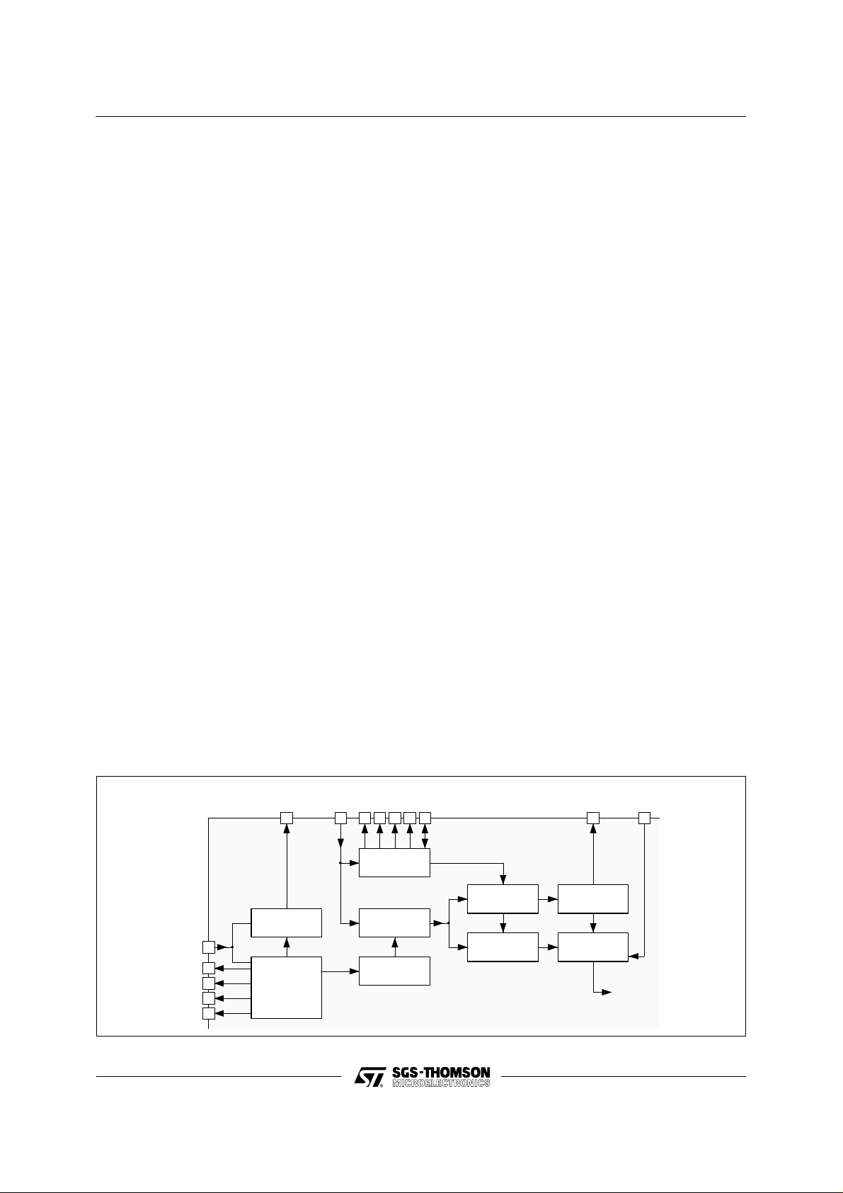
FUNCTION DESCRIPTION
The TDA8204B is partitioned into 6 major parts
shown in the block diagram.
The NICAM Decoder performs data and sound
recovery from the signals specified in
EBU SPB 424. The ex panded digital audio signals
(14-bit) are made available at the digital audio
interface (I
2
S) in a serial multiplex of left and right
channels. They are also processed by a 4 times
upsampling digital filter and noise shaper which
results in a high speed digital data stream at the
output pins DACD L/DACDR. This data s tream c an
be applied to the 1-bit D-A convert ors contained i n
the TDA8205.
The TDA8204B is I
2
C bus controlled and provides
control over the functions of the TDA8205 by
means of a serial inter-chip bus.
1 - NICAM Decode r
1.1 - BLOCK DI A GR AM (see Fi gure 3)
1.2 - DESCRIPTION
NICAM frame alignment requires searching out a
frame alignment word (FAW) and a 16 frame sequence conveyed by C0 bit. Because of noise,
interferences, errors in the incoming NICA M Data,
aliases of the FAW, a robust scheme is implemented. It ensur es the decoder will align, and st ay
aligned, to signals beyond the limit of maximum
useable error rate. Thank s to a 511 bit PRBS synchronized by the recovered clock and a modulo 2
adder, original data are recovered. This data
stream can be processed externaly for de-encryption in Pay TV applications using descr ambled data
Pins DDO, DDI.
To allow simultaneous reading and writing of
mono/stereo samples , de-interleaved data frames
are stored in a 3 page RAM.
TDA8204B
The 10-bit input audio samples are expanded to
14-bit using scale factor bits according to NICAM
decoding rules. Samples in error by the parity
check are replaced by interpolated one or repeated.
Mute is set accor ding to an er ror count er w hen t he
error rate exceeds error rate limit (ERL) and reset
when the error rate is below ERL/4.
Application cont rol inform ation (bit C1, C2, C3, C 4)
is recovered by majority decision logic over 16
frames. the C1, C2, C3 , C4 bits can be read in SR0
register and are set on the C1, C2, C3, C4 pins
according to the state of bit 0 (BEA) of the CR2
register.
2 - Digital Filter an d Noise Sh ap er
A digital filter performs 4X upsampling in two
stages. The main FIR 2x upsampler is followed by
a smaller 2x FIR upsampler. Digital upsampling
means a much simpler post-DAC reconstruction
filter can be used thus saving on external component count and cost.
A noise shaper converts the samples from the
digital filter into two high speed serial bitstreams
which can be applied to the DA Cs in the TDA8205.
2
3 - I
S Bus
A standard three-wire interface, conforming to the
2
S bus protocol, is provided, allowing connection
I
of an external DAC or DA T interf ace. Audio samples
contain 14-bit, so 16-bit DACs will pad the t wo LSBs
with 0. The word select clock operates at 32kHz
and the serial clock at 896kHz.
By setting SDI bit of CR2 to 1, the I
receive the digital I
2
S sound. This prevents dupli-
cating the dual D/A converter.
2
S interface ca n
Figure 3 : NICAM Decoder Block Diagram
DDI
NDI
PDV
DV
FID
ADV
DDO
DESCRAMBLER
39
30
33
29
31
FRAME
CONTROL
C1C2C3
21 20 19 18 62728
MAJORITY
LOGIC
3 PAGE
RAM
ADDRESS
GENERATOR
C4
RSW
SCALE FACTOR
RECOVERY
EXPANDER
ER
23
ERROR
COUNTER
CONCEAL
AND MUTE
MUTE
25
TO FILTER
8204B-05.EPS
5/12

TDA8204B
4 - Interchip Bus
A one-line serial bus provides interchip communications allowing control of all functions t hrough the
single I
5 - I
An I
2
C bus interface.
2
C Bus
2
C bus interface provides access to control and
status registers within the two chips t o allow control
of their f unct ions and monitoring of s t atus . A digital
filter is inclu ded to improve noise immunity.
5.1 - DATA F LA GS (s ee Figure 4)
These indicate the status of the descrambled dat a
on the DDO pin. They are inhibited if the decoder
is out of alignement.
- FID : Frame alignment word (scrambled)
- PDV : Parity Data V alid. CIB0 and CIB1 overwrit e
the first 2 bits of FAW
- ADV : 11 addit io nal data bits
- DV : Data valid (mode dependant)
5.2 - DECRYP T ION (s ee Figur e 5)
The PRBS generator (used for descrambling) is
normally preset to all ones at the start of each
frame. However, it is possible to preset it to any
value on each frame by means of a code word clock
Figure 4 : Data Flags
(CWC) and serial code word data (CWD) interfac e
on pins SEL0 and SEL1.
CWD, which is clocked in on the n egative going
edges of the CWC clock, can be sent anywhere
during the frame except when FID = 1. The CWC
is asynchronous with respect to the Nicam clock
and the CWD will be used on the following frame.
During the time FID = 1, the levels on the SEL0,
SEL1 pins are read for language selection. Code
words for descrambler presetting may be sent in
either an 8-bit or 9-bit formats. There are four
possibilities :
- if 7 or less clock cycles are counted on CW -clock
during a frame, the PRBS generator is preset to
all ones ;
- i f 8 clock cycles are counted, 8 bits of CW-data
are clocked into the shif t register , the first bit of the
previous transfer now moving to bit 9 position in
the shift register. The resulting value is used to
preset the PRBS generator on the next fram e.
- if 9 clock cycles are counted, t he CW-data (whic h
has been clocked into a 9-bit shift register) is used
to preset the PRBS generator on the next frame.
- i f 10 or more clock cycles are counted, only the
first 9 bits of the CW-data are used and loaded
into the PRBS generator on the next fram e.
CK728
DDO
FID
PDV
ADV
DV Stereo
DV Mono
DV Data
CB0 CB1
FAW
Figure 5 : PRBS Preset ter
FID
SEL0
(CWC)
SEL1
(CWD)
C0 C1 C2C3C4
AD0
1 FRAME NEXT FRAME
AD10
NICAM DATA 704 BITS
24 CONTROL
EVEN FRAME
ODD FRAME
704 DATA
8204B-06.EPS
8204B-07.EPS
6/12

TDA8204B
5.3 - SOFTWARE SPECIFICA TION
Software control of IC’s is given by programming
four registers, one read only status register (SR0)
and three read and write control registers (CR1,
CR2, CR3).
Transm it format : S = Start, A = Acknowledge
P = stop
S
ADDRESS
CHIP
0A
REG SUB
ADDRESS
A DATA A P
Receive format :
CHIP
S
ADDRESS
Note : All registers are read sequentially; device status and the
contents of all registers may be read. The sequence may be
terminated by not acknowledging (NOACK) the slave.
1A
SR0
DATA
A
CR1
DATA
AP
Chip address
1 01101HAOR/W
MSB LSB
HAO : Hardware address select ion pi n
Register addresses
Reg.
Name
SR0 00000000NICAM status
CR1 00000001Matrix and mutes
CR2 00000010NICAM control
CR3 00000011Switches
Sub Adress Function
Register cont ent s
SR0 : NICAM status (read only)
US2 C1 C2 C3 C4 MUT LA2 L/S
US2 0 0 0 1 1 1 1
MSB LSB
L/S : • If FN1 bit of CR2 is 0, LS bit is loss of
frame alignment status
LS =1, FAW is lost
LS = 0 FAW is identified
• If FN1 bit of CR2 is 1, LS bit is selected
system status
LS = 1, B/G standard
LS = 0, I standard
LA2 : Loss of sub-frame alignment
(1 = loss of alignment)
MUT : NICAM mute (1 = DAC outputs muted)
C4 : Reserve sound flag (1 = FM backup)
C3 : Application control bit 3
C2 : Application control bit 2
C1 : Application control bit 1
US2 : User bit 2 (input)
US2 bit indicates the state of US2 input Pin
CR1 : Matrix and m ut es (read and writ e regist er)
Q1 Q0 I2 I1 I0 G0 AUM FRE
00000000
MSB LSB
Qn : Output select (see tables)
In : Input select (see tables)
G0 : Auxiliary output gain, 0 = 0dB, 1 = 6 dB
AUM : Auxiliary output mute, 0 = no-mute,
1 = muted
FRE : Free run clock VCXO for set up,
0 = normal, 1 = fr ee ru n
To set crystal ser ies capac itor
Switches and Matrix Description
Figure 6
LFIL1
RFIL1
SAIL
MAI
SAIR
AMOL
AMOR
INTL
INTR
Audio matrixReserve sound switch
EAIL
EAIR
38 3732 3136 3534
2728AOL
AOR
Output selection
Q1 Q0 Output
0 0 AOL
0 1 AOR
Mute and gain selection
Q0 I2 Mute Gain
0 0 OFF* 0 1 ON* 1 0 - 0dB**
1 1 - +6dB**
* Mute is activated by left channel selection
** Gain is activated by right channel selection
Input selection
I1 I0 Input
0 0 INTL
0 1 INTR
1 0 EAIL
1 1 EAIR
Example of programming
First
step
: 0 0 1 0 0 X X X
INTL connected to AOL, mute ON on
AOL/AOR
Sec-
ond
step
Thrird
step
: 0 1 0 1 1 X X X
EAIR connected to AOR, gain 0dB on
AOL/AOR
: 0 0 0 0 0 X X X
INTL connected to AOL, mute OFF on
AOL/AOR
The power up default configuration is 0dB and
unmute for both channels AOL/R, and INTL connected to AOL, and INT R connected to AOR.
8204B-08.EPS
7/12

TDA8204B
CR2 : NICAM cont rol (re ad and write register)
SDI ECT MAE FN1 UMT LA1 LA0 BEA
00000001
MSB LSB
SDI : I2S direction
0 = Output, 1 = Input
ECT : Bit error rate counting time
0 = 128ms, 1 = 64ms
MAE : Max allowed errors
0 = 511, 1 = 255
FN1 : Set function of bit 0 in SR0, 0 = loss of
alignment (status), 1 = system status (I or
B/G)
UMT : Un-mute NICAM, 1 = un-mute, 0 = mut e
LA1 :
LA0 :
Language select 1 (LA1 ⊕ SEL1)
Language select 0 (LA0 ⊕ SEL0)
BEA : Set C1-C3 function
ECT MAE BER MUTE
0 0 8.9 x 10
0 1 4.4 x 10
1 0 1.8 x 10
1 1 8.9 x 10
-3
(1 in 112)
-3
(1 in 225)
-2
(1 in 56)
-3
(1 in 112)
Un-mute at BE R /4.
TDA8204B
Output (Pin)
C1 (21) C1* Single mono mode
C2 (20) C2* Dual mono mode
C3 (19) C3* Stereo mode
01
BEA
* Application control bit of NICA M signal
Note : C4 pin remains unchanged. The function of C1-C4 in SR0
remains unchanged.
CR3 : Switches (r ead and write regis ter )
US1 US0 AUT IBG FS1 FS0 X SYN
00100001
MSB LSB
US1 : User bit 1 (output)
US0 : User bit 0 (output)
AUT : Automatic select ion, 1 = enable
IBG : Select system I or B/G, 1 = B/G
FSn : Force switch (see table)
SYN : 1 = synthesiser, 0 = dual VCXO
(carrier loop)
FS1 FS0 Selection
0 0 Auto NICAM
0 1 FM-Mono
1 0 FM-Stereo
1 1 NICAM
NICAM S TAND-ALONE AP PL IC ATION
The NICAM kit has been designed to be m onitored
by the I
2
C bus; nevertheless stand-alone working
capability is offered to the designer for low cost
applications.
In order to know the status of the kit in stand-alone
mode, consider the contents of the four I
2
C registers at power-ON (4 registers : SR0 - CR1 - CR2 CR3). Hardware configurable pins will be described
later.
1 - Power-ON Configuration
SR0 (status)
US2 C1 C2 C3 C4 MUT LA2 L/S
US2 0 0 0 1 1 1 1
MSB LSB
US2 : Not used in stand-alone
C1 :
C2 :
C3 :
Application control bit status for
NICAM signal
C4 : Reserve Sound Flag
MUT : DAC outputs muted (demuted as soon
as NICAM appears)
LA2 : the subframe alignment is been lost
L/S : FAW status (FN1 of CR2 = 0)
CR1 (R/W)
Q1 Q0 I2 I1 I0 G0 AUM FRE
00000000
MSB LSB
Q1 :
Q0 :
I2 :
NICAM sound is sent on all matrix
outputs and on AMOx pins
I1 :
G0 : Gain = 0dB on AMOx
AUM : AMOx pins un-muted
FRE : VCXO in normal mode
CR2 (R/W)
SDA ECT MAE FN1 UMT LA1 LA0 BEA
00000001
MSB LSB
SDA : Normal mode
ECT &
: BER = 1/112
MAE
FN1 : Bit L/S of SR0 set to alignment loss
status
UMT : TDA8204B mute pin 25 to 0
LA1 : Result depending of SEL1
LA0 : Result depending of SEL0
BEA : Beacon decoding mode but all diodes
are OFF until a NICAM signal has been
found
CR3 (R/W)
US1 US0 AUT IBG FS1 FS0 X SYN
00100001
MSB LSB
US1 : Not used in stand-by mode
US0 : Not used in stand-by mode
AUT : Automatic standard
8/12

IBG : Standard I (don’t care)
FSn : Set to Auto NICAM (if NICAM fails, FM
mono is select ed)
FN2 : Not used
SYN : Synthesizer selected
2 - Hardware Config urab le Pi ns
2.1 - TDA8204B - PIN 6 - (RSW)
- as an output :
status of the RSW switch
- 0 = FM mono
- 1 = NICAM
- as an input :
- 0 = FM mono (forced)
2.2 - TDA8204B - PINS 34/35 - (SEL0/ S EL1)
(see Figure 7)
- to select the language in case of bilingual opera-
tion
- selected value is related to LA0 and LA1
Figure 7
TDA8204B
2
As the I
(power-ON condition) / SEL0 = Q 0, S EL1 = Q 1
The 4 choices are summarized in the table below.
M1 = Mono 1
M2 = Mono 2
VII - 2.3. TDA8204B - PIN 25 - (MUTE )
- as an output :
- as an input :
C bus is not used LA0 and LA1 = 0
SEL0 SEL1 DACDL DACDR
0 0 M1 M2
0 1 M1 M1
1 0 M2 M2
1 1 M2 M1
status of the DAC
- 0 = unmuted
- 1 = muted
- 0 = unmute DAC (forced)
SEL1
34
SEL0 35
LA0 LA1
Q1 = SEL1 LA1
Q0 = SEL0 LA0
Q1
Q0
S
W
I
T
C
H
8204B-09.EPS
9/12

TDA8204B
APPLICATION DIAGRAMS
Figure 8 : Stand Alone Application (I standard)
LED2LED3LED4
6.8nF
6.8nF
DAC
(forced)
Unmute
stereo
Q1, Q2 : BC109 or BC550C
F1 : TOKO TH316BQM2110QDAF (5VFP)
T1 : Matsushita EFCS6R0MWS
X1 : 11.648MHz Crystal NDK
Ω
R20 22k
F
µ
C26
220
H
µ
F
L2 10
µ
C23
10
DD
H
µ
10
C6
220pF
V
CC
V
AUDIO
OUTPUT
R
L
FM MONO IN
Language
ERROR
MONITOR
Selection
LK1 LK2
LED1
Ω
R17 330
F
µ
C21
10
F
µ
C20
10
F
F
µ
µ
C24 1
C25 1
C19
100nF
22
23
27 26 25 24
28
29
35 34 33 32 31 30
36
37
mute
41 40 39 38
42
Ω
22
26 25 24 23
27
28
29
35 34 33 32 31 30
36
IC1 TDA8205 IC2 TDA8204B
21
16 17 18 19 20
15
14
C28
100nF
8 9 10 11 12 13
7
2 3 4 5 6
1
R19 270
21
17 18 19 20
16
15
14
Ω
Q2
8 9 10 11 12 13
7
single
FM mono
C17 100nF
R11 5.6k
C13
mono
(forced)
100nF
dual
mono
Ω
R16
1M
F
µ
C16
10
C18
Ω
100nF
C15
R15
5.6k
Ω
R14
43k
Ω
R13
43k
Ω
C14
R12
5.6k
L1
MON2
MON1
10/12
40 39 38 37
41
C10 6.8nF
Ω
R10 39k
42
C9 120pF
C8
220nF
Ω
R9 8.2M
C7
100nF
X1
11.648MHz
C11 150pF
C12 18pF*
* C12 value depends on X1
3 4 5 6
2
R18 10kW
1
Ω
C7 680pF
R8
150
C4 1nF
F1
BFP
6.552MHz
C3 10nF
Ω
R4
470
Ω
R1
8.2k
C5
Ω
220pF
R7
470
Ω
R6
33
Ω
C2 10nF
R5
100
Q1
TRAP
Ω
R2 470
C1
NICAM
Ω
R3
1.2k
10nF
IN
SYS. I
F
µ
C22
10
T1
6.0MHz
8204B-10.EPS

Figure 9 : I2C Bus Controlled Applicatio n (I and B/G standard)
mono
LED2
LED3
DD
V
22
ERROR
MUTE
FID
PDV
ADV
DV
SEL1
SEL0
TEST
CK728
MONITOR
25 24 23
26
28 27
29
30
31
DD
32
V
33
34
35
36
37
38
39
Ω
mute
LED1
R25
DD
V
F
µ
C19
10
F
µ
C18
AUDIO
10
OUTPUT
Right Left
F
µ
C17
1
330
42 41 40
R32 270
Ω
22
26 25 24 23
27
F
µ
1
C16
Left
F
µ
C15
AUDIO
STEREO
EXTERNAL
10
Right
MUTABLE OUT
F
µ
C14
10
IN
FM
MONO
C13
100nF
C12
100nF
AUDIO IN
Right Left
C11
100nF
Left
C10
AUDIO IN
Right
C9
* C23 value depends on X1
100nF
100nF
X1
11.648MHz
C22 150pF
C23 18pF *
28
29
31 30
32
35 34 33
36
37
IC1 TDA8205 IC2 TDA8204B
38
42 41 40 39
C26
C21 6.8n F
C25
R1 39kΩ
220nF
R27 8.2MΩ
CC
V
Ω
120pF
R2
150
single
21
18 19 20
17
15 16
14
13
12
11
10
9
8
7
6
5
4
1 2 3
21
17 18 19 20
C42 100nF
16
15
14
12 13
11
8 9 10
7
6
R23 5.6k
Ω
Q3
C39
5
R31 10kΩ
1 2 3 4
F1
C45 680pF
R5
R6
TDA8204B
C BUS
2
I
dual
mono
C43
100nF
C37 1nF
5.85MHz
C32 10nF
Ω
470
8.2kΩ
SDA
SCL
LED4
stereo
C1
C2
C3
BITS
CONTROL
C4
WS
SCK
S BUS
SD
2
I
GND
US0
US1
BITS
USER
RSW
Q1, Q2, Q3 : BC109 or BC550C
F1 : TOKO TH31 6 BQM 2080 QDAF (5VFP)
F2 : TOKO TH31 6 BQM 2110 QDAF (5VFP)
T1 : M atsushita EFCS5R5MWS
T2 : M atsushita EFCS6R0MWS
X1 / 11 .64 8M Hz C ry s tal ND K
Ω
R24
1M
F
µ
C20
10
100nF
Ω
C41
R22
5.6k
Ω
R21
43k
Ω
R20
43k
Ω
C40
R19
5.6k
DD
V
R17
470Ω
BFP
C33 10nF
Q1
TRAP
R7 470Ω
C31
10nF
IN
NICAM
SYS. BG
CC
V
Ω
R33 22k
6.8nF
F
µ
6.8nF
C44
220
33Ω
Ω
100
Ω
1.2k
F2
T1
5.5MHz
R10
R9
R8
+12V
DD
V
C4
100nF
C3
100nF
C2
100nF
F
µ
C1
10
C38 1nF
6.552MHz
C35 10nF
Ω
R11
470
Ω
R12
8.2k
C8
100nF
C7
100nF
C6
100nF
F
µ
C5
10
+5V
MON1
MON2
C29
220pF
C30
Ω
R18
470
BFP
C36 10nF
Q2
R13 470 Ω
TRAP
220pF
R16
33Ω
Ω
R15
100
T2
6.0MHz
Ω
R14
1.2k
C34
IN 10nF
SYS. I
NICA M
8204B-11.EPS
11/12

TDA8204B
P ACKAGE MECHANICAL DATA
42 PINS - PLAST IC SHRI NK
a1
e4
F
A
I
L
b1
e
Stand-off
22
21
E
Dimensions
b2
b
e
D
42
1
Millimeters Inches
Min. Typ. Max. Min. Typ. Max.
A 3.30 0.130
a1 0.51 0.020
b 0.35 0.59 0.014 0.023
b1 0.20 0.36 0.008 0.014
b2 0.75 1.42 0.030 0.056
b3 0.75 0.030
D 39.12 1.540
E 15.57 17.35 0.613 0.683
e 1.778 0.070
e3 35.56 1.400
e4 15.24 0.600
F 14.48 0.570
i 5.08 0.200
L 2.54 0.100
PMSDIP42.EPS
SDIP42.TBL
Information furnished is believed to be accurate and reliable. However, SGS-THOMSON Microelectronics assumes no responsibility for the consequences of use of such information nor for any infringement of patents or other rights of third parties which may
result from its use. No licence is granted by implication or otherwise under any patent or patent rights of SGS-THOMSON Microelectronics. Speci fica tions mentioned in this publicati on are subject to change without notice. This publication supersedes and
replaces all information previously supplied. SGS-THOMS ON Microelectronics products are not authorized for use as critical components in life support devices or systems without express written approval of SGS-THOMSON Microelectronics.
© 1994 SGS-THOMSON Microelectronics - All Rights Reserved
2
Purchase of I
2
C Patent. Rights to use these components in a I2C system, is granted provided that the system conforms to
I
Australia - Brazil - China - France - Germany - Hong Kong - Italy - Japan - Korea - Malaysia - Malta - Morocco
The Netherlands - Singapore - Spain - Sweden - Switzerland - Taiwan - Thailand - United Kingdom - U.S.A.
C Components of SGS-THOMSON Microelectronics, conveys a license under the Philips
2
C Standard Specifications as defined by Philips.
the I
SGS-THOMSON Microelectronics GROUP OF COMPANIES
12/12
 Loading...